
W/Ti�Ͻ�вļ����Ʊ�����
������ɫ�����о���Ժ������Դ��ұ������о���,������ɫ�����о���Ժ������Դ��ұ������о���,������ɫ�����о���Ժ������Դ��ұ������о���,����������ѧ�������������о�����,������ɫ�����о���Ժ������Դ��ұ������о��� ����100088,����������ѧ�������������о�����,����100029,����100088,����100088,����100029,����100088,����������ѧ�������������о�����,����100029
ժ Ҫ��
������W/Ti�Ͻ���ɢ�赲���ڼ��ɵ�·�������е����ü�Ӧ�������������W/Ti�Ͻ�вĵ����Բ���-����ܶȡ��۽ṹ����������, ��W/Ti�Ͻ�Ĥ����֮��Ĺ�ϵ, ָ�����ܶȡ��ߴ��ȡ���Ti�ຬ���ٵĺϽ�в����Ʊ�����W/Ti�Ͻ���ɢ�赲�㱡Ĥ�Ļ����������������Ʊ�W/Ti�Ͻ�вĵ�3�ַ���-�����ѹ������������ѹ���ȵȾ�ѹ, �������˲�ͬ�����Ʊ��İв������ϵIJ���, �����Ʊ�������W/Ti�Ͻ�вĵĹ���������
�ؼ��ʣ�
��ͼ����ţ� TN405
�ո����ڣ�2005-04-20
����������Ȼ��ѧ���� (50501003) ������Ŀ;
Tungsten-Titanium Targets and Manufacturing Technology
Abstract��
The application of tungsten-titanium diffusion barrier layer in the integrated circuit was presented.The relationship between tungsten-titanium sputtering target characteristics, density, microstructure, metal purity and film performance, was reviewed.Target material with high density, high purity, low content of Ti rich �� phase is a fundamental reqirement to produce films with good quality.Hot press and hot isostatic press methods used to fabricate tungsten-titanium sputtering targets were introduced.Properties of W-Ti sputter targets made by different methods were summarized.
Keyword��
sputtering target;diffusion barrier layers;hot press;
Received�� 2005-04-20
Ŀǰ���ɵ�·��������Ҫ�д�ͳ��Al���ߺ����˵�Cu��������, ��Al��Cu����ʲ�Si��SiO2����ɢ�ٶȺܿ�, ���ǽ���Si��SiO2�л�䵱���ܼ������ʵĽ�ɫ, ʹ�����������ܴ�����½�, ��˱����ȡ��Ч��ʩ��ֹ����ɢ, ���ڽ��ʲ�Ͳ��߽���֮������һ����ɢ�赲��
������ɫ�����о���Ժ��20����90������ڿ�ʼ�з����ֽ���в�, ���е����й��Ƽ����Ĺ��ҹ�����Ŀ���Ƚ���ѧ��Ĥ�����øߴ�ϡ���� ϡ�н������仯������Ʊ������о� (2004DFBA0003) ��, �Ը��۵���� (W, Ta) ���Ͻ� (W-Ti, TeFeCo, DyFeCo) �вĽ����Ʊ����������� ������Ҫ����W/Ti�Ͻ�в����ܲ��������Ʊ�������
1 W/Ti�Ͻ���ɢ�赲�����
Ӧ���ڼ��ɵ�·�е���ɢ�赲�㰴�������õĻ��ƿɷ�Ϊ: �ȶ��͡� ��Ӧ�͡� �����3��
������W/Ti�赲����Al�������е�Ӧ��Ϊ�������������û��ơ� ��W/Ti�Ƿ�Ӧ����ɢ�赲��, ����Al�������з�Ӧ
Ti+3Al�� TiAl3 (400 ��)
W+12Al�� WAl12 (450��500 ��)
�÷�Ӧ�൱����, ����ֻҪW/Ti�㹻��, δ��Ӧ�㽫���ֽӴ��ȶ���, Ȼ��������ɢЧӦʹ��W/Ti�赲������450��500 ��, 30 min�˻�������ʧЧ
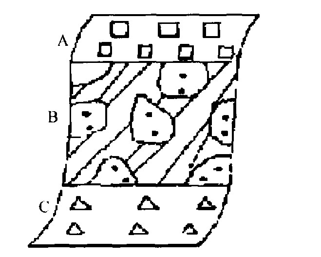
ͼ1 W/Ti�Ͻ���ɢ�赲��ʾ��ͼ B-W/Ti�Ͻ�; A-Al��Cu; C-Si��SiO2
Fig.1 Sketch of tungsten-titanium diffusion barrier layers
2 W/Ti�Ͻ�в����ܲ���
Ӱ��W/Ti�Ͻ�Ĥ���ܵ����غܶ�, ������Ĥ�ļ���������� ��Ĥ�ɷ���ɡ� ��Ĥ�����ʺ͵�Ǩ���Լ�������Ⱦ��, ��Ŀǰ, ��ԼW/Ti�Ͻ�Ĥ���ܵ���Ҫ������������Ⱦ (���ñ�Ĥ����������λ�����Ĥ�ϵĿ�������������)
2.1 ����ܶ�
������ĩͨ����ѹ�ս�ɿ�״�вĺ�, ��������ֳ���ṹ�� �вĵĿ�϶�ʿ���ͨ������в�����ܶȴ�С��ȷ����, ����ܶ�Խ���϶��ԽС�� W/Ti�Ͻ�вĵ�����ܶȸ��ݻ�е���ԭ�����, ��ʽ����:
�����ܶ�=100/ (wt%W/��w+wt%Ti/��Ti)
����ܶ�=��ʵ�ܶ�/�����ܶ�
����: wt%W, wt%Ti-W��Ti�������ٷֱ�; ��w, ��Ti-W��Ti���ܶ�
Udler D��
2.2 �۽ṹ
W/Ti�Ͻ�в���W��Ti�����γɵĹ�����ṹ�� ��W/Ti�Ͻ���ͼ�����ڲ�ͬ����ɺ��¶���, W/Ti�Ͻ��ָ��ӵ���̬�ṹ, ��ͼ3��ʾ
Ti���۵���1670 ��, ��������, TiΪ������������Ħ���, ���¶����ߵ�885 ��ʱ, Ti����ͬ������ת��, ��Ϊ������������Ħ���; W���۵���3407 ��, �����µ����۵�ʱ��Ϊ����; Ti������10%��20%֮��, ��һ���¶ȷ�Χ��W/Ti�Ͻ��ɦ�1 (Ti, W) �ͦ�2 (Ti, W) �������, ��1 (Ti, W) ��ָ��Ti������, ��2 (Ti, W) ָ��W�����塣
Dunlop J��
2.3 ��������
Ŀǰ�������˾�������ߴ��ȵ�W/Ti�Ͻ�в�, ����MRC��˾������ULTRA, ULTRA 2, ECLIPSE 3��W/Ti�Ͻ�в�, ���1��ʾ��
�о�����W/Ti�Ͻ�вĽ�������Խ��, �����Ĥ��Ĥ������Խ��
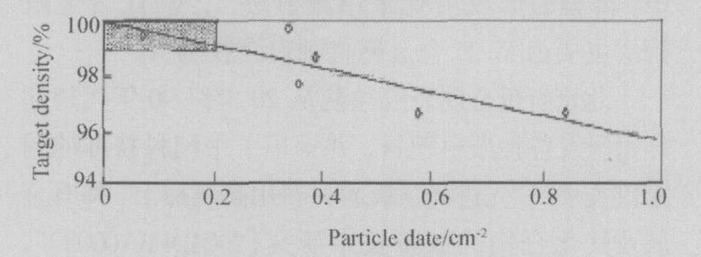
ͼ2 �в�����ܶ����������Ĺ�ϵ
Fig.2 Relationship between target density and particle counts
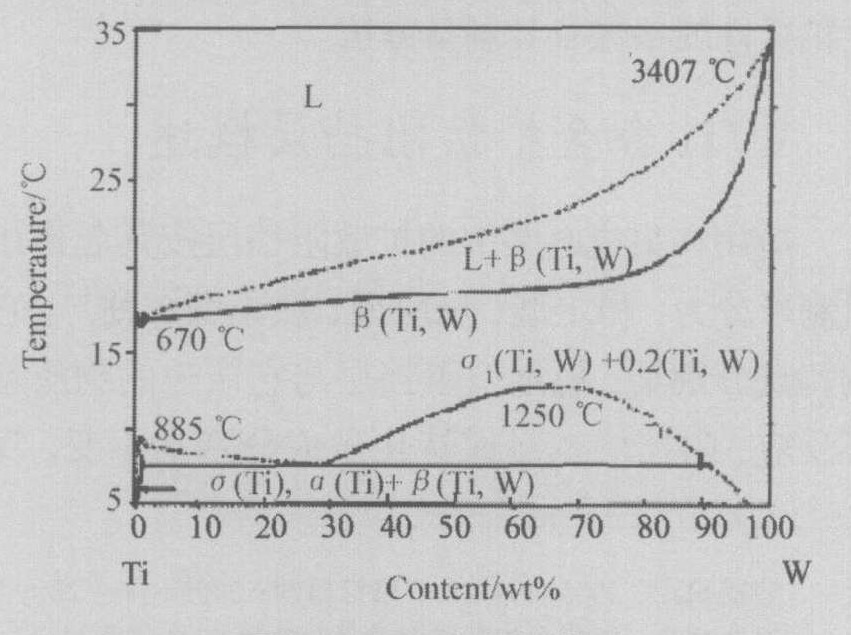
ͼ3 W/Ti�Ͻ���ͼ
Fig.3 Tungsten-titanium phase diagram

ͼ4 ���������1 (Ti, W) �ຬ���Ĺ�ϵ
Fig.4 Relationship between particle counts and content of ��1 (Ti, W) phase
��1 MRC������W/Ti�Ͻ�вĵĽ����������ܶ�
Table 1Metallic impurities and density of targets manufactured by MRC
W/Ti�Ͻ�в� |
ULTRA | ULTRA2 | ECLIPSE |
��������/% |
99.99 | 99.995 | 99.9975 |
��С����ܶ�/% |
95 | 97 | 97 |
3 W/Ti�Ͻ�вĵ��Ʊ�����
�����Ͻ��Ʊ�ͨ�������������� ����W/Ti�Ͻ�вĵ��Ʊ�ȴ�����ڲ��ø÷���, ԭ��������: һ, W���۵�ߴ�3407 ��, Ŀǰ���豸���Ѵﵽ��˸���; ��, W��Ti����ѹ���̫��, �������������ѿ��ƺϽ�ɷ���ɡ� Ŀǰ, �Ʊ�W/Ti�Ͻ�вĵķ�����Ҫ����ѹ�����ȵȾ�ѹ��, ������ѹ�����������ѹ���Ͷ���������ѹ��
3.1 �����ѹ��
�����ѹ�������ڽϵ��¶����Ʊ��dz����ܵIJ���, ���Ҳ��Ͼ�����֯���ȡ� ǿ�ȸߵ��ŵ�
3.2 ����������ѹ��
�������ѹ��������, ֻ��ģ����Χ�Ļ�����ͬ, ����������ѹ��ͨ��������塣 �����ַ��������Ա�����������������������ʽӴ�������Ⱦ, ���ǵļ�ѹ��ʽ����ͨ������ģ��������ѹ���� Snowman A��
3.3 �ȵȾ�ѹ��
�ȵȾ�ѹ (HIP) ��һ����ǰ���ļ���, Ϊ���ϵ����ܻ��ṩ������Ч�ķ���
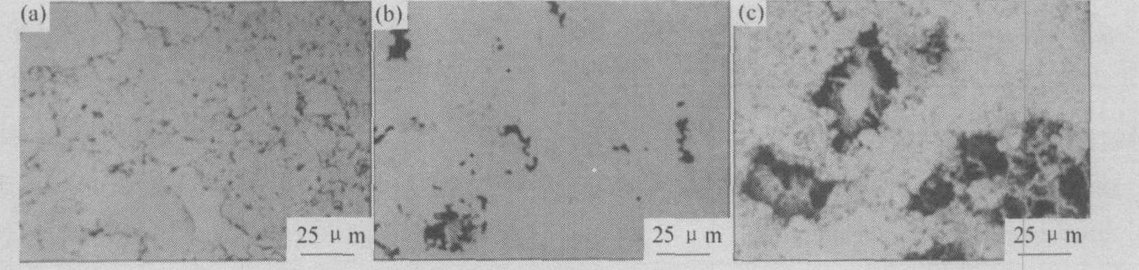
ͼ5 W/Ti�вĵ羵��Ƭ
Fig.5 Optical micrographs of W/Ti target materials
�ȵȾ�ѹ�� (a) 775 ��; (b) 1000 ��; (c) 1550 ��
Waterman E��
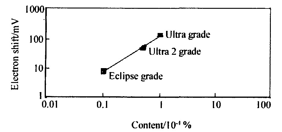
ͼ6 ����� (K, Na, Li) �������Ǩ�ƵĹ�ϵ [16]
Fig.6 Relationship between alkali (K, Na, Li) content and electron shift
��2 �в����Բ����빤������ [21]
Table 2 Target properties and manufacturing condition
�в� |
A | B | C | D | E |
ѹ��/MPa |
30 | 100 | 100 | 100 | 100 |
�¶�/�� |
775 | 1000 | 1180 | 1550 | 1180 |
�ܶ�/ (g��cm-1) |
14.48 | 14.52 | 14.37 | 14.08 | 14.23 |
��1 (Ti, W) ����/% |
0 | 17 | 32 | 100 | 32 |
�����ܶ�/ (particles��cm-1) |
0.07 | 0.33 | 0.38 | 0.83 | 0.35 |
��3 3���Ʊ�����������������
Table 3Difference of manufacturing conditions among three manufacturing techniques
�Ʊ����� |
��ѹ��ʽ | ѹ�� | �¶� |
�����ѹ |
���� | �� | �� |
����������ѹ |
���� | �� | �� |
�ȵȾ�ѹ |
����ѹ�� | �� | �� |
Wickersham C E��
4 �� ��
�ɸ��ܶȡ� ��1 (Ti, W) �ຬ���ټ��߽������ȵ�W/Ti�Ͻ�в��Ƶõ���ɢ�赲��, ������Ч����ֹ���߽��� (Al��Cu) ��Si��SiO2����ɢ, �Ӷ���������ȶ���, �ƶ��뵼�幤ҵ�ķ�չ�� Ŀǰ, ��Ժ���Ʊ������ܶȡ� ��1 (Ti, W) �ຬ����Խ��ٵ�W/Ti�Ͻ�в�, �ðвĵ�����ܶ��Ѵﵽ����ˮƽ, ����1 (Ti, W) �ຬ�������в�ࡣ ��һ�������ǶԦ�1 (Ti, W) ������Ļ��Ƽ��������о�, ��1 (Ti, W) ��IJ���Ϊһ��ɢ����, ֻҪ����W��Ti����ɢ�Ϳ��Խ��ͦ�1 (Ti, W) �ຬ��, ������ͼͨ������ѧ�Ͷ���ѧģ�����, ��ȷ��һ����ѵĹ����¶�, �Ӷ����ͰвĦ�1 (Ti, W) �ຬ����
�����
[1] ������.ͭ�������豸[J].���ӹ�ҵר���豸, 1999, 28 (3) :13.
[2] �Ź���, ����, ������, ��.ULSI��ͭ���������Ĺؼ�����[J].����ѧ, 2001, 31 (2) :146.
[3] ����Ӣ, ��.ULSI�Ʊ���ͭ���ߵ������⼼��[J].�뵼��ѧ��, 2003, 24 (4) :433.
[4] �Ӷ���, �־�, ���ٲ�, ��.ͭ���߹������赲����Ĥ���о�[J].�������ѧ�о����չ, 2002, 22 (1) :78.
[8] ������, �ؼ̺�.����в�����[J].�Ϻ�����, 2002, 4:30.
[9] ������, ��־��, ��ΰ��, ��.�뵼������ŷķ�Ӵ��е���ɢ�赲��[J].����ѧ������, 1998, 5:53.
[18] Massalski T B.Binary Alloy Phase Diagrams[M].Metals ParkOhio:American Society for Metals, 1990.
[25] л��, ����, ��.�����ѹ�������Ʊ�CuCr�Ͻ��е�Ӧ���о�[J].����ұ��, 2002, 31 (1) :38.
