

Novel preparation of big bulk-nanocrystalline Cu in large quantities
CHU Guang(�� ��)1, 2, TANG Yong-jian(������)2, LIU Wei(�� ΰ)2, 3, YANG Tian-zu(������)1
1. School of Metallurgical Science and Engineering, Central South University, Changsha 410083,China;
2. Research Center of Laser Fusion , China Academy of Engineering Physics, Mianyang 621900, China;
3. School of Science and Engineering, Southwest University of Science and Technology,Mianyang 621010, China
Received 29 December 2005; accepted 19 May 2006
Abstract:
The micrometer-sized Cu powder produced on commercial scale was compacted under pressure of 1.0-2.0 GPa and at room temperature,and the nanocrystalline(nc) Cu with diameter of 10 mm and thickness of 8 mm, relative density of 99.4% of the theoretical density for pure Cu (8.96 g/cm3), and mean grain size of 34-43 nm and microstrain of 0.16%-0.19% was obtained. The compacting process was analyzed with HUANG Pei-yun equation and the microstructure and properties of nc Cu were studied by XRD, SEM, PAS, MHV2000 mircrohardness tester and Datron 1081-type electrometer. The results show that the grain size of nc Cu samples is correlated with compacting pressure, the microhardness is 1.14-1.27 GPa which is about two times larger than that of the coarse-grained polycrystalline Cu, but the relationship between microhardness and grain size do not obey Hall-Petch equation strictly. The electrical resistivity of the specimens is 5.1��10-7��?m, larger than the coarse-grained Cu materials by a factor of 29, the mean lifetime of positron-annihilation is (172.8��0.8) ps. The cost of the method of fabrication for big-sized nc material is much lower than that of any others. This method has the advantages such as the lowest cost, largest output and volume as well as highest density over all other methods so far.
Key words:
nanocrystalline Cu; synthesis; method; microhardness; electrical resistivity; Hall-Petch equation;
1 Introduction
Bulk nanocrystalline(nc) metals, in which the grain is in nanometer range, often have some interesting properties such as increased hardness and strength, unique electronical and optical properties,which would open up a range of new applications[1, 2]. These remarkable mechanical properties of nc materials are highly desirable for structural application. To optimize the mechanical behavior, it is important to produce big-sized bulk nc metal materials in a way of lower cost and in large quantities. The nc metals can be prepared in several ways, among the most common of which are high-pressure compactin of nanometer-sized cluster and high-energy ball milling[3, 4]. But the two kinds of methods have many shortcomings such as the higher cost of fabrication and the smaller size of products, which can not be put into production. Therefore a lower cost method of preparation of an ��ideal��and big nc metal materials has been seeking since a German scientist, GLEITER, presented the concept of nc material and fabricated the nc material for the first time at the beginning of 1980s[5].
Recently a new and lower cost method for preparation of big and almost fully dense bulk-nc Cu in large quantities has been invented by the authors. The nc Cu samples, with a diameter of 15 mm and thickness of 8 mm, were successfully consolidated by micrometer-sized Cu powder produceded on commercial scale under pressure of 1.0-2.0 GPa within 3 s. The pressure was held at this value for 5 min at room temperature then released within 2 s.
The X-ray diffraction(XRD) analysis, scanning electron microscope(SEM), positron annihilation spectroscopy(PAS), MH2000 microhardness tester and Datron 1081-type electrometer(made in England) were used to determine and investigate the average grain size and mean lattice strain, the microstructure, micro- hardness and electrical resistivity of as-consolidated nc Cu samples. The results shows that the as-consolidated Cu spencimens possess really many properties of nano-sructural materials, and the cost of this method of fabrication for big-sized nc material is much lower than that of any others.
2 experimental
The micrometer-sized Cu powders (so-called M-P) were produced on commercial scale by means of some process. The Cu nanoparticles (so-called N-P) were synthesized by a so-called flow-levitation method[6]. The purity of both Cu powders is about 99.9% (mass fraction, %). The nc Cu specimen (with diameter of 15 mm and thickness of 8 mm) were prepared from M-P under pressure of 1.0-2.0 GPa and at room temperature. The density of nc Cu samples was measured to be 8.91 g/cm3 by means of Archimedes, principle, which is equivalent to 99.4% of the theoretical density of pure Cu(8.96 g/cm3).
Quantitive XRD measurements of the nc-Cu samples were carried out in a Philips X Pert Pro MPD X-ray diffracometer with Cu K�� radiation. X-ray wave- lengths K��1=0.154 05 nm and K��2=0.154 44 nm were selected by using a graphite monochrometer. The average grain size and microstrain were determined in terms of Warren�CAverbach Fourier transfer analysis[7]. Calibration of the instrumental line broadening was performed by using the standard SiO2 sample. SEM experiments were performed on a JEM-5900 scanning electron microscope at operating voltage of 20 kV.
Vickers microhrdness measurements were conducted in as-prepared specimens at room temperature with diamond indenter of 2.0 N load for 10 s. Hardness was measured along the diameter of the specimens. Four different regions were sampled to obtain the average hardness of each specimen.
Datron 1081-type electrometer was used to measure the electrical resistance at low temperature (233-293 K). The space of temperature is 10 K. The samples are 10 mm in length, 1 mm in width and thickness respectively.
The measurements of the lifetime spectra of positron annihilation were performed for nc samples. The positron lifetime spectra were recorded using a fast-fast coincidence setup with a time resolution (FWHM) of 260 ps for 60Co ��-rays accepted under experimental windows.
3 Results and discussion
3.1 Effect of compacting pressure on density
Fig.1 gives the relative density of nc Cu samples as a function of compacting pressure. It can be seen from Fig.1 that relative density of either nc Cu made from M-P or N-P increases with increasing pressure. But in the process of compacting, the tendency of densification between them is different. Under 0.76 GPa and 1.5 GPa, the relative density (relative to conventional poly-crystalline Cu) of nc-Cu made from M-P is between 98.5% and 99.4%. But under the same pressure, the relative density of nc-Cu made from N-P is only 86.4%- 93.2%. Fig.1 shows that it is more difficult to consolidate N-P than M-P.
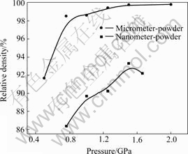
Fig.1 Relationship between density and pressure for micrometer-sized powders and nanometer-sized powders respetively
According to HUANG Pei-yun equation, if function of compacting pressure is Y, the density of as-consolidated Cu sample is X, then
![]() (1)
(1)
Y=lgp (2)
The compacting equation is
Y=mX+b (3)
or
Y=mX+lgM (b=lgM) (4)
where dm is the density of full dense alloy; d0 is the loose density of powder before compacting; d is the density of green compact; p is pressure; m is the slope of the compacting equation (index of hardening); b is the intercept of compacting equation; M is the compacting modulus.
According to the above equations, the data in Fig.1 were calculated. The calculated results of X and Y were summarized in a plot of X vs Y. The slope and intercept were obtained by a least-square fit of the profile and listed in Table 1.
It can be seen that the value of m of M-P is about 10 times larger than that of N-P, illustrating that the hardening tendency of N-P is smaller when compacted, on the other hand the value of M of N-P is 104 times
Table 1 Results of pressure and density function at different pressures and linear regression results of compacting equation

larger that of M-P. The value of M is related with the property of compaction of powder in some extent, including the loss of compacting pressure. It can be seen that in the course of compacting, the friction between nano-particles and the mould wall is very large and results in larger loss of compacting pressure.
3.2 Microstructural characterization
Fig.2 shows the X-ray diffraction patterns for M-P and nc Cu samples made from M-P respectively. XRD analysis in terms of Warren�CAverbach Fourier transfer analysis indicated an average grain size of nc Cu samples before and after compacting under different pressure (Table 2). Cuprous oxide was not detected by means of XRD.
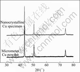
Fig.2 X-ray diffraction patterns of micrometer-sized Cu powder before and after compacting under 1.2 GPa and at 25 ��
Table 2 Relationship between grain size and pressure
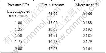
From Table 2, it can be clearly seen that the average grain size and microstrain are influenced by the compacting pressure, when the compacting pressure is smaller than 1.5 GPa, the average grain size decrease from 43.02 to 34.51 nm with the increasing pressure, when the pressure is larger than 1.5 GPa, the average grain size increases from 34.51 to 42.25 nm.
The researchers discovered that for larger grain size (but still in nanometer scale), grain boundaries start to emit partial dislocations[8], full dislocations have been observed in simulations of columnar microstructures with grain sizes of 30 nm. In this experiment, the grain size of M-P was 52 nm, plasticity was fully determined by dislocation activity[9]. Therefore the reason for grain refinement is that when the samples were compacted with the temperature increasing, the recovery and recrystallization probably happened and then refined grains were obtained. If the compacting pressure remained to be increased, the temperature of samples would rise and the grain would start to grow.
The mean microstrain of as-compacted nc Cu samples was determined by XRD[10], being about 0.164%-0.192%. Such a large microstrain in the as-compacted sample is a signature of high level dislocation density at grain boundaries(GBs), which induces a remarkable lattice distortion in the vicinity of GBs.
The positron lifetime spectra of the samples were best resolved into two components, designated as ��1 and ��2, and with relative intensities I1 and I2. Based on the data of the fitted lifetime spectra , we obtained ��1=(170.5��0.4) ps, ��2=(2 334.1��367.2) ps with the respective intensities of 99.88% and 0.121%, which exibits that a mean lifetime of positron-annihilation is (172.8��0.8) ps. It may be suggested that the microdefect of the nc Cu samples contains mostly vacancies and almost no vacany-cluster-like volumes and larger voids, We note that the value of mean lifetime is lower than that of the nc Cu by any other method of preparation[11]. The nearly full density of the as-consolidated Cu sample was verified by positron annihilation spectroscopy measure- ments.
Section-view SEM observations as shown in Fig.3 shows that the as-prepared Cu samples consist of spherical particles (with particle size of 10-20 ��m) contacting each other firmly and there are almost no pores in samples. Because there is no preparation of nano-particles, various artifacts such as porosity and contamination are not introduced. The artifacts have significant effects on the mechanical properties as well as deformation mechanism.
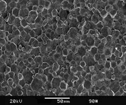
Fig.3 SEM image of nanocrystalline Cu made from M-P under 1.2 GPa and at 25 ��
3.3 Effect of grain size on microhardness
Grain size is known to have a profound effect on the mechanical behavior of materials, in particular, on the yield stress and hardness. The Hall-Petch relationship [12] is a well-known expression relating the variation in yield stress to the grain size of a material:
��y=��0+kd-1/2 (5)
where ��y is the yield stress, ��0 is the lattice friction stress required to move individual dislocation, k is a constant and d is the grain size. The form of the equation indicates that a decrease in grain size will lead to an increase in the yield strength. According to the Hall-Petch equation, large yield strengths may be attained by reducing the grain size of materials. For example, a drop in average grain size from 10 ��m to 10 nm should increase the yield stress by more than thirty-fold.
For pyramidal indenters, hardness(HV)of metals is empirically related to the yield stress(��0) by the relation HV/��0��3. It follows that for material that exhibits Hall-Petch behavior, hardness(HV) should be related to grain size(d) by
HV=H0+kHd1/2 (6)
where H0 and kH are constants. The experimental results of hardness for the nc Cu samples with the average grain size ranging from 34 to 43 nm (obtained from X-ray diffraction) were summarized in Fig.4 as a plot of mean hardness (HV) vs d-1/2.
The microhardness of nc Cu samples ranged from 1.14 to 1.27 GPa, which is about two times larger than that of the coarse-grained polycrystalline Cu. The relation between microhardness and grain size does not obey the Hall-Petch equation strictly. When d is larger than 36 nm, the microhardness no longer increases and levels off the equation with a drop in grain size. It may indicate a change in the deformation mechanism, or it may result from differences in process necessary to obtain small grain size[13]. The crystallites sliding along grain boundaries or the grain boundary diffusion creep are possible deformation mechanism for the materials with ultrafine grains[14].
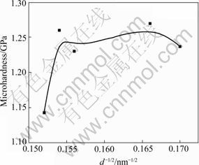
Fig.4 Relationship curve of grain size and microhardness
3.4 Electrical resistivity
The electrical resistivity of nc metals was first studied by GLEITER et al[15], they found that resistivity of nc Pd, Cu and Fe was higher than the coarse-grained metals. There is a large volume fraction of grain boundary in nanostructured materials and electron activity is confined to small grain size range. The thicker is the grain boundary, the more atoms in material are in a state of disorder. Subsequently the electron scattering becomes stronger. For a grain sizes larger than the electron mean free path, the resistivity deviates considerably from the corresponding bulk values. In other words, electron scattering by volume scattering effects inside the crystals occurs and becomes the dominant scattering mode suggesting a high density of point or line defects in the crystallites. It results in the high resistivity of nanocrystalline metals. Fig.5 shows the temperature (233 K-293 K) dependence of electrical resistivity of nc Cu samples made from N-P and M-P respectively. It can be clearly seen that for each sample the resistivity relates linearly with the temperature. At room temperature,the resistivity of the nc Cu made from M-P is 5.1��10-7��?m, about 3 times larger than the nc Cu made from N-P , 2-3 times larger than that in Ref.[16], and larger than the coarse grained Cu materials by a factor of 29. This results may be due to differences in microstructure and process of nc Cu samples obtained.
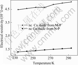
Fig.5 Temperature dependence of electrical resistivity of nc Cu samples cinoacted under 1.2 GPa and at 25 ��
4 ConclusionsThe nc Cu samples using M-P as the starting material have been successfully prepared by cold pressing method of micrometer-sized powders, with a diameter of 15 mm and thickness of 8 mm, relative density of 99.4%, microhardness of 1.14-1.27 GPa, grain size of 34-43 nm, electrical resistivity of 5.1��10-7��?m at room temperature and the average positron annihilation lifetime of (172.8��0.8) ps.
References[1] ROCO M C, WILLIAMS R S, ALIVISATOS P, et al. Nanotechnology Research Directions [M]. Kluwer, Dordrecht, Netherlands, 2000.
[2] SIEGEL R W. Encyclopedia of Applied Physics [M]. New York: VCH, 1994(11): 173-199.
[3] SIEGEL R W. What do we really know about the atomic-scale structure of nanophase materials [J]. J Phys Chem Solids,1994, 55: 1097-1106.
[4] LU L, SUI M L, LU K. Cold rolling of bulk nanocrystalline Copper [J]. Acta Mater, 2001, 49: 4127-4134.
[5] LI C M, LEI H, TANG Y J, et al. Production of copper nanoparticles by the flow-levitation method [J]. Nanotechnology, 2004, 15: 1866-1869.
[6] GUO L H, LI H. Fabrication and characterization of thin nano- hydroxyapatite coatings on titanium [J]. Surface & Coatings Technology, 2004, 185: 268-274.
[7] van SWYGENHOVEN H. Grain boundaries and dislocations [J]. Science, 2002, 296: 67.
[8] van SWYGENHOVEN H. Grain boundaries and dislocations [J]. Science, 2002, 296: 67.
[9] QIAN L H, LU Q H, KONG W J. Electrical resistivity of fully-relaxed grain boundaries in nanocrystalline Cu [J]. Scripta Mater, 2004, 50: 1407-1408.
[10] ZHANG Li-de, MOU Ji- mei. Nanomaterials and Nanostructure [M]. Beijing: The Science Press, 2002. 216-221.
[11] NIEMAN G W, WEERTMAN J R. Mechanical behavior of nanocrystalline Cu and Pd [J]. J Mater Res, 1991, 6(5): 1012-1027.
[12] SANDERS P G, EASTMAN J A, WEERTMAN J R. Elastic and tensile behavior of nanocrystalline copper and palladium [J]. Acta Mater, 1997, 45(10): 4019-4025.
[13] LU K, WEI W D, WANG J T. Microhardness and fracture properties of nanocrystalline Ni-P alloy [J]. Scripta Metal Mater, 1990, 24: 2319-2323.
[14] GLEITER H. Nanocrystalline materials [J]. Prog Mater Sci, 1989, 33: 223-315.
[15] QIAN L H, LU Q H , KONG W J, LU K. Electrical resistivity of fully-relaxed grain boundaries in nanocrystalline Cu [J]. Scripta Mater, 2004, 50: 1409-1410.
(Edited by LONG Huai-zhong)
Foundation item: Project(10475069/A0506) supported by the National Natural Science Foundation of China
Corresponding author: CHU Guang; Tel: +86-731-8836791; Fax: +86-731-8710171; E-mail: user12134@sina.com
