
�뵼�弯�ɵ�·�ý����軯����Ʊ���������
������ɫ�����о���Ժ�Ƚ����Ӳ����о���
ժ Ҫ��
�����軯��㷺�������������е�Դ��©��դ��������缫��ĽӴ�, ���Ʊ������ɵ�·�Ĺؼ�����֮һ�����������˰뵼�弯�ɵ�·�ù��ܽ����軯�������ɡ����淴Ӧ���γɻ����Լ�������������ע�롢������������������ӵȶ����Ʊ��������Ƚ���TiSi2, Co-Si2, NiSi�IJ������ʼ���Բ�ͬ�����ڵ㼯�ɵ�·���ܵ�Ӱ�졣�������˻��¶���NiSi����ṹ�;�������Ĺ�ϵ��������ϡ�������軯����������պ����ĵ����ݼ��������ԡ����������������軯�������������ȱ��, ���ȶ��Եļ�ⷽ����������Ϊ, ̽��32 nm�����¼����ڵ㼫���ģ�뵼�弯�ɵ�·�����ͽ����軯���ѳ�Ϊ����о�����������
�ؼ��ʣ�
��ͼ����ţ� TN304
�ո����ڣ�2009-06-01
����Dow-Coning���ʺ�����Ŀ����;
Preparation and Characterization of Metal Silicides Used for Semiconductor Integrated Circuits
Abstract��
Silicides are widely used as the contacts for the source, drain and gate in CMOS devices, which are also the key materials for nanoscaled integrated circuits.The phase structures, interfacial reaction, formation mechanism, as well as manufacture processing technologies such as thermal evaporation, sputtering, ion implantation and molecular beam epitaxy (MBE) were reviewed.Material properties of TiSi2, CoSi2, NiSi and effects on the device performance at different technology nodes were presented.The relationship between annealing temperatures and the lattice structures and constants of NiSi were analyzed.The growth techniques, the barrier states and the interfaces for rare earth silicides were thoroughly described.The measurement approaches and characterization on properties, defects and thermal stability of the silicides were discussed.Finally, it is worth noting that an investigation for new alternative silicides is needed for sub-32 nm advanced VLSI.
Keyword��
metal silicides;property;detection;defect;silicon technology;
Received�� 2009-06-01
�����軯����������õĸ������Զ��㷺Ӧ���ڵ���Ԫ�����¿�����Ϳ��
1 �����軯���γɻ����о�
������֪, �ڹ�/������������ͼ��, ͨ������3, 4�ֻ����Ĺ軯���ࡣ ������Ĥ��������һ����γɵ�ĿǰΪֹʼ���DZȽ��ѽ���Ŀ��⡣ ����, Ti/Siϵ����4�ֲ�ͬ�ľ��� (Ti5Si3, TiSi, C49-TiSi2��C54-TiSi2)
ʵ����, ��Ŀǰ����ȷ��;��һ�ٶ��ֽ����軯����, ��������� ��������� ���ۺ�ϡ�������軯������ڼ��ɵ�·�� ��1�г���2008�����µĹ��ʰ뵼�弼��·��ͼ (ITRS) ���ڽ����軯��IJ��ּ���ָ��
��1 2008������ITRS���ڽ����軯��IJ��ּ���ָ��
Table 1 Part of the latest ITRS technology index for metal silicides of 2008
Year |
2009 | 2010 | 2011 | 2012 | 2013 | 2014 | 2015 |
Max. of silicon wafer diameter/mm |
300 | 300 | 300 | 450 | 450 | 450 | 450 |
MPU physical gate length/nm |
41 | 35 | 31 | 28 | 25 | 22 | 20 |
MPU gate length/nm |
27 | 24 | 22 | 20 | 18 | 17 | 15 |
Xj/nm |
29.0 | 26.7 | 24.7 | 22.0 | 19.8 | 18.6 | 16.9 |
Thickness of silicides/nm |
17.9 | 16.2 | 14.7 | 13.0 | 12.0 | 11.5 | 10.3 |
Silicides thin layer resistance/ (����sq-1) |
9.1 | 9.9 | 10.8 | 12.1 | 13.5 | 14.4 | 15.8 |
����, �����軯����������ѧ���ݶ����˽����������ķ�Ӧ������Ҫ�� ����������軯��������¶�Զ���ںϽ��¶ȡ� �����軯��������ȿ�������ɢ������ (�����ʱ���ƽ����������) , Ҳ�����ǽ��淴Ӧ������ (�����ʱ�������) �� ���ʺ���Ⱦ������Ӱ��軯��������ٶȡ� Cheng��
2 �����軯����Ʊ�����������
����ܶ�����������γ��ȶ��Ļ�����, ��Щ�軯�����ҪӦ��֮һ������ΪMOS�����ĵ缫�Ӵ����������ϡ� �ر��ǵ����ɵ�·�Ĺ���߿������׳߶ȷ�չʱ, �����軯����ϸ�Ϊ���ɻ�ȱ�� ��2�г��˼����ڼ��ɵ�·��ҵ�г��õĽ����軯��ĺϽ��¶Ⱥ͵����ʲ����� ��3�Ƚ��������ɵ�·����Ҫ�����軯������ܡ� ���ڽ��ֱ�������ǵ��Ʊ����պ����ԡ�
ͼ1������Polycide��Salicide���չ���ʾ��ͼ��
Polycide���չ��� (ͼ1 (a) ) : ͨ���ڸ�����, ʹ�øߴ������ۺϽ�в�, ��WSi2, TaSi2��MoSi2�Ƚ��н���, ��Щ�����軯�ﲻ�����ȶ����ҿ���ѧ��ʴ�� Salicide�Զ��軯�﹤�չ��� (ͼ1 (b) ) : �����Ʊ��ྦྷդͼ�κͲ�ڵĶ�������������������; Ȼ���������ṹ�ϳ�������Ti��Co, �ٽ��п����ȴ���, �γɽ����軯��TiSi2��CoSi2, ��һ��Ҫ�ر�С�ı���¯�ڵ�����Ⱦ; ������ѡ����ʪ����ʴ������Ҫ�Ľ�����ȥ�� ���Ƴ̴���С�˽Ӵ����� (ͼ2) ��
��2���ɵ�·��ҵ�м��ֳ��ý����軯��ĺϽ��¶Ⱥ͵�����
Table 2Alloy temperature and resistance of some metal silicides in IC industry
| Silicides | Minimum of eutectic temperature/�� |
Formation temperature/�� |
Resistance/ (����m) |
CoSi2 |
900 | 600��700 | (13��19) ��10-8 |
MoSi2 |
1410 | 900��1100 | (40��70) ��10-8 |
PtSi |
830 | 700��800 | (28��35) ��10-8 |
TaSi2 |
1385 | 900��1100 | (35��55) ��10-8 |
TiSi2 |
1330 | 600��700 | (13��17) ��10-8 |
WSi2 |
1440 | 900��1100 | 31��10-8 |
��3 �뵼�������ɵ�·����Ҫ�����軯�����ܱȽ�
Table 3Comparison of primary metal silicides using in semiconductor nano IC industry
| Silicides | C54-TiSi2 | CoSi2 | NiSi |
Technique node/nm |
>180 | 180��90 | ��65 |
Formation temperature/�� |
600��700 | 600��700 | 400��600 |
Film resistance/ (����m) |
(13��20) ��10-8 | (14��20) ��10-8 | (14��20) ��10-8 |
Height of Schottky barrier/eV |
0.60 | 0.64 | 0.67 |
Alternative corrosive |
NH4OH:H2O2 | HCl:H2O2 | HNO3:HCl |
Si consumption proportion |
2.27 | 3.64 | 1.83 |
Melting point/�� |
1500 | 1326 | 992 |
Alloying temperature/�� |
1330 | 1204 | 964 |
Hot stable temperature/�� |
<950 | 900 | 700 |
Stress/ (109 dyn��cm-2) |
15��25 | 8��10 | 1 |
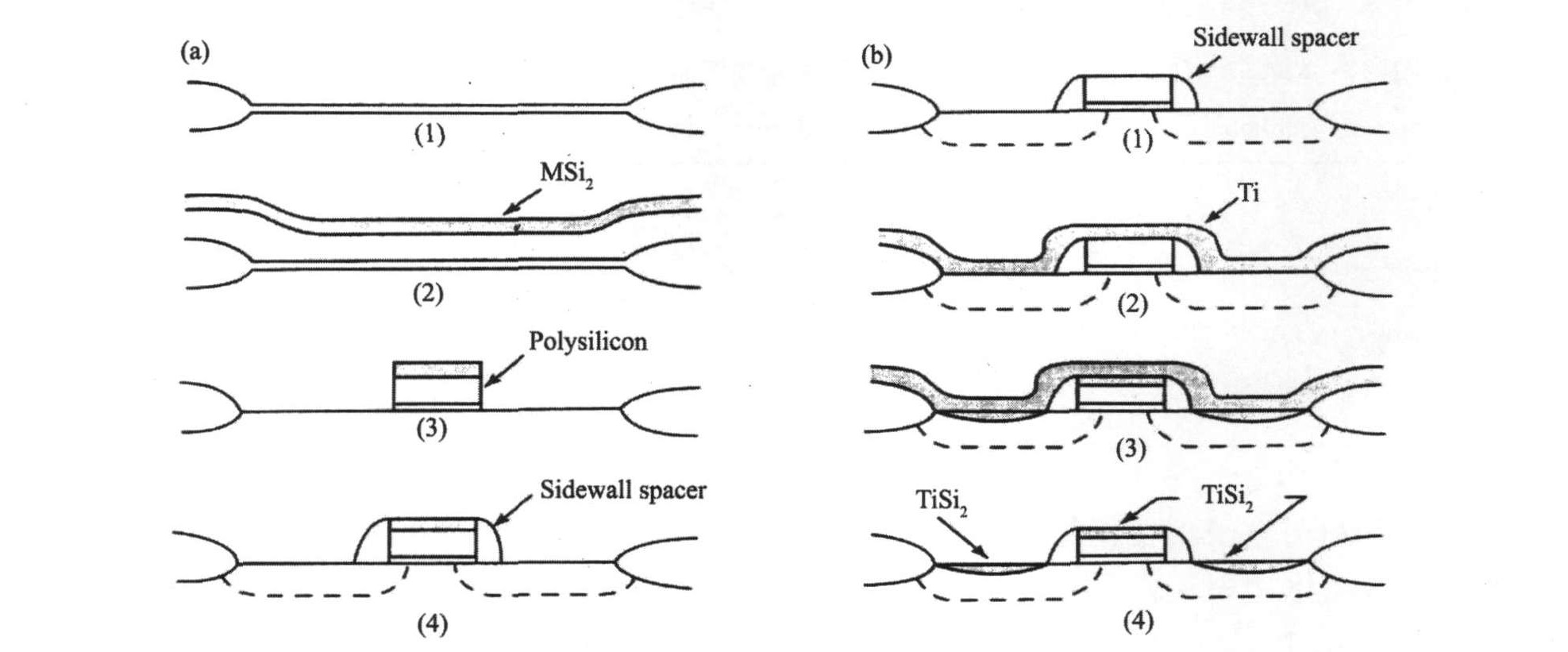
ͼ1 Polycide��Salicide���չ���
Fig.1 Polycide and Salicide process
(a) Polycide process: (1) gate oxide, (2) depositing poly silicon and silicide, (3) polycide patterning, (4) gate, source, drain ion implant; (b) Salicide process: (1) gate patterning and source ion implant, (2) depositing metal (Ti, Co) , (3) formation of silicide by annealing, (4) removing unreacted metal by selective wet etching technique
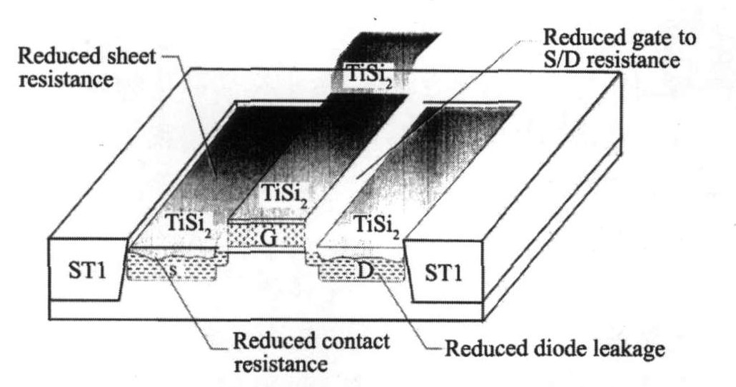
ͼ2 �Զ��軯�ѸĽ���ѧ����ʾ��ͼ
Fig.2 Pattern of self-aligned Ti silicide improving electronic property
2.1 TiSi2��CoSi2
TiSi2���Ʊ����ձȽϼ�, ���Ȳ��øߴ��Ѱ�ͨ�����������ڹ�Ƭ�ϳ����ѽ������㡣 ��600��700 ���һ���˻��õ�����C49�м���, Ȼ���ٽ��еڶ����˻�, �¶���800��900 ��֮��, �����γ�����Ҫ��C54�ࡣ TiSi2�ȿ���Ϊ�����ĵ缫�ͻ�������, �ֿ���Ϊ����ע����赲��, �Լ�С����ע�����ȡ� ������n��ĵ���ͨ��TiSi2�����p������ע������γ�dzpn�ᡣ ��ĵ���ע������״��������Ӱ��TiSi2�ı�����̬�� ʵ��֤�������������ڹ�ĵ��ϸ���TiSi2�� B��Fͬʱ���ڻ����Լ���TiSi2��Ĥ������ò�� C54-TiSi2��ȱ���Ǵ����߿�ЧӦ, ���߿��ͽӴ������Сʱ, TiSi2��������, ��ת���¶�Ҳ����ߡ� �����ɵ�·�ٽ��߿���Сʱ, ���ܳ���TiSi2��䲻��ֶ����½Ӵ�������������� ���, ���ʺ�����0.25 ��m���µļ��ɵ�·�Ƴ̡�
CoSi2�����߿�ЧӦ���ɹ�����0.25 ��m��90 nm�����ڵ�ļ��ɵ�·�Ƴ̡� ����, ������һ��Si (001) ��ĵ���B+, BF+2, As+��P+ע���Si (001) ��Ʒ, ֻҪ��600��900 ���˻�1 h, �����������������CoSi2��Ĥ�� �����1000 �����˻�1 h, �������Ʒ���γ����Ե�С���� ��CoSi2��ȱ�������γɹ軯��ʱ���Ĺ�϶�, ����ڶ����˻���¶���700 ���������������45 nm���µ��Ƴ̡� ����, �̹���ЧӦҲ�Խ����軯����ȵ�����������ϸ��Ҫ��
2.2 ϡ�������軯��
����ϡ�������軯����о�ʼ��1980�ꡣ 1981��, Tu��
��4 ϡ�������軯����n-Si (100) �ĵ��ϵĺϳɹ����������������
Table 4 Synthesis technology and basic physical property of rare earth silicide on n-Si (100) substrate
Silicides |
Height of Shottky barrier |
|||||||||
| GdSi2 | ErSi2 | DySi2 | HoSi2 | YSi2 | ||||||
| ��b/eV | 0.39��0.06 | 0.39��0.06 | 0.37��0.06 | 0.37��0.06 | 0.39��0.06 | |||||
Thin layer resistance (��/sq) |
6.60 | 2.44 | 6.50 | 5.90 | 4.30 | |||||
Formation temperature and time |
300 ��, >1 h | 350 ��, >24 h | 325 ��, ��2.5 h | 350 ��, >2 h | 325 ��, >8 h | |||||
Crystal structure |
Orthogonal | Hexagonal | Orthogonal | Hexagonal/Orthogonal | Hexagonal/Orthogonal | |||||
Knapp
ϡ�������軯����Թ���ϲ����нϵ͵�Ф�ػ����� (��n����0.3��0.4 eV, ��p����0.7��0.8 eV) ������Si (111) �ĵ���ʧ���С (��0.75%) , �������ʵ����ν�Ķ�άϡ�������軯������������ ����, ErSi2����Si (111) ����������� (ML) ��, ��500 �����˻��γ�1��1�ṹ�Ķ�ά�軯��
Ŀǰ, ���ڼ��ɵ�·��ϡ�������軯������������ ����ע�롢 ��������� ���������ӵȶ����Ʊ�����, һ����Ҫ�����ʵ��ĺ������ա� �������������Ʊ�ϡ�������軯�����Ϻ��˻���̡� ���÷����ܵ����ٽ��¶ȡ����� (�˴����ٽ��¶ȡ�ָϡ��������Ĥ�ڹ�����˻��γɹ軯�����ʼ�¶�) �� ���ڴ��¶�, ���γ�ϡ�������軯� �á��ٽ��¶ȡ�һ��Ϊ300��350 ��, ���Ʊ�����Ʒ�����Ϊ�ֲ�, ͬʱ��Si/ϡ�������軯�������ڴ����ṹȱ���Լ�����ʧ�䡣 ����, ϡ�������軯�����ױ�����, ��Щ���������˸�������Ĥ���Ʊ���Ӧ�á�
����ע�뼼��ͻ����ƽ���������ڹ��в�Er���ܽ������, ��ʵ��ϡ�����ӵĸ�Ũ�Ȳ��ӡ� ��������ע�����������, ���γɴ�����������ϡ�������軯�����, Ŀǰ�ѳ�Ϊ���з�չǰ���Ĺ軯���Ʊ�����֮һ�� Benton
��Ƶ���䷨���и�Ч�ʡ� �ͳɱ����ŵ�, �ұ�Ĥ��ȡ� ���������������ơ� ����ϡ��Ԫ����Si�ĸ��ϰл����������ϰ��ܹ��Ʊ�������ϡ�������軯�ﱡĤ�� Kim��
���������� (MBE) �����������������γɵ�ϡ�������軯�ﱡĤ��Ʒ��, �����ַ���Ҫ��ߴ�ϡ�������� �߽ྻ��ĵױ����Լ�������ա� Ŀǰ��MBE�����Ʊ�����ϡ�������軯�ﻹû�еõ��㷺Ӧ�á�
2.3 NiSi
NiSi���˻��¶�һ����600 ������, Զ����TiSi2��CoSi2�� ��Ȼ�������軯��������Բ��������˻�, ����һ�μ���˻��������������˻�ʱ��, �������������ɵ�·�Ƴ̵�Ҫ�� ��CoSi2���, NiSi����û���߿�ЧӦ (ͼ3) ; ���γɹ�����Ҫ����ԭ����ɢ���������Ĺ�, ��˽����˽Ӵ����衣 ʵ�����NiSi�γɵĽ���Ӧ��Ҳ��С��
NiSi��ȱ����Ҫ��������: һ�������������γ���״ȱ��, ������̬�ֲ�, ����©��������; �������¶Ȳ�ͬ�����ֲ�ͬ�����, ��Ni2Si��, �ڸ���700 ������ɸ���NiSi2�ࡣ ����, NiSi���к�ǿ��������������; �ڹ�ĵ��Ͽ��γ�����֯��, �ڸ����»����γ�NiSi2��������, �����ž�ʹ��Ĥ������
NiSi����б����ṹ�� Rabadanov��
a=0.5187-1.807��10-5T+6.026��10-8T2-
2.709��10-11T3 (1)
b=0.3286+2.977��10-5T-6.557��10-8T2+
2.915��10-11T3 (2)
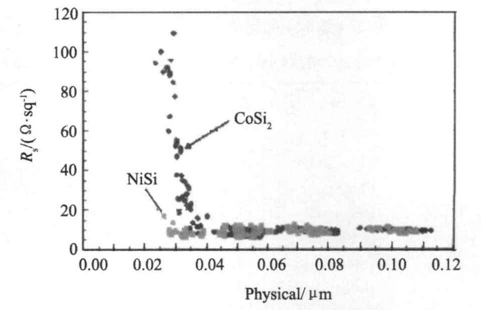
ͼ3 CoSi2��NiSi�������߿��ı仯ͼ
Fig.3 A linewidth dependence function of CoSi2 and NiSi resistance
c=0.5626-1.779��10-5T+5.727��10-8T2-
2.546��10-11T3 (3)
���ڱ�Ĥ��Ʒ��˵, D��Heurle��
��ȻNiSi���нϵ͵��ȵ��ʡ� �����ʺ�©����, ���ѳ�Ϊ�����ɵ�·�Ϻõ�Դ�� ©�� դ���ĽӴ�����
��ͼ4�ɿ���, Ni/Si��ͼ����11����, ������Ni3Si, Ni31Si12, Ni2Si, Ni3Si2, NiSi��NiSi2��6���������������ȶ���
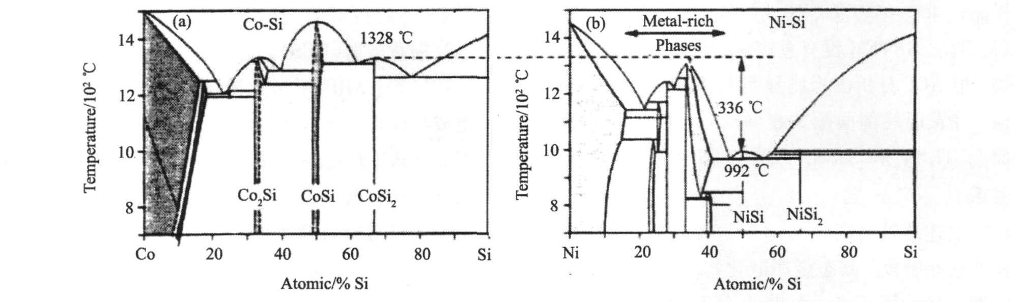
ͼ4 Co/Si (a) ��Ni/Si (b) ��ϵ��ͼ�Ƚ�
Fig.4 Phase diagram of Co/Si (a) and Ni/Si (b) system
��5 Ni, Ni/Si���Si�ľ���ṹ�ıȽ�
Table 5 Comparison of Ni, Ni/Si and Si crystal structure
| Phases | Crystal structure |
Silicides t/Ni t |
Crystal constant/nm |
Si consumption/ Nit |
Density/ (g��cm-3) |
Ni |
Cubic | - | 0.35238 | 0 | 8.91 |
Ni3Si |
Cubic | 1.31 | 0.35056 | 0.61 | 7.87 |
Ni31Si12 |
Hexagonal | 1.40 | 0.6671/1.2288 | 0.71 | 7.56 |
Ni2Si |
Orthorhombic | 1.47 | 0.739/0.990/0.703 | 0.91 | 7.51 |
Ni3Si2 |
Orthorhombic | 1.75 | 1.229/1.0805/0.6924 | 1.22 | 6.71 |
NiSi |
Orthorhombic | 2.20 | 0.5233/0.3258/0.5659 | 1.83 | 5.97 |
NiSi2 |
Cubic | 3.61 | 0.5416 | 3.66 | 4.80 |
Si |
Cubic | - | 0.54309 | - | 2.33 |
��6 �������ȶ��������軯������
Table 6 Stable Ni based silicide properties at room temperature
| Phases | Resistance/ (10-8 ����m) |
Melting point or phase change temperature/�� |
Average E/GPa |
Average CTE of films/ (10-6 K-1) |
Formation enthalpy/ (kJ��mol-1) |
Ni |
7��10 | 1455 | 200 | 13.4 | - |
Ni3Si |
80��90 | 1035/1170 | 139 | 9.0 | 149 |
Ni31Si12 |
90��150 | 1242 | 177 | - | 1850 |
Ni2Si |
24��30 | 1255/1306 | 161 | 16.5 | 132��143 |
Ni3Si2 |
60��70 | 830/845 | 167 | - | 224-232 |
NiSi |
10.5��18 | 992 | 132 | 212.0 | 85��90 |
NiSi2 |
34��50 | 981/993 | - | - | 87��94 |
Si |
Depending on doping | 1414 | 130��187 | 2.60 | - |
3 �����軯���������ȱ�ݼ������
�����軯��ļ�����۰�����Ĥ����ṹ�� ��ѧ�ɷ֡� ������ò�� ����̬����ѧ�� ��ѧ���ԡ� ���ȶ��Ժ���ȱ�ݵȡ�
3.1 �Ǿ�������еĽ����軯��ɺ˼��
������ͨ���߷ֱ�羵 (HRTEM) ��Ͽ��ٸ���Ҷ�任 (FFT) ���Զ��������� (ACF) ������ڷǾ������������Ľ����軯��ɷ֡� ����, Ti/Si��Ʒ��400��450 ��, 60 s�Ŀ����˻� (RTA) ���̺�, ͨ��HRTEMû��ֱ�ӹ۲쵽��״�Ľ����軯��, ��ACF����ͼ������ʾ�и��ܶȵ������Խṹ, ������������ͼ��������ͽDz������ݷ�����Ti5Si3��Ti5Si4��TiSi���нϺõĶ�Ӧ��ϵ
������������ش�����һ����Ϣ, �����淴Ӧ�ij�ʼ��, ��̬�����軯��̫С����HRTEMӰ������ʾ������, ������ACF��������, ֤�����ڳ�ʼ�λ��γɶ����м�̬�����軯� ��Щ�۲��붯��ѧ����ģ��˵����������ӽ��ľ�̬��ֺͽṹ���ȳɺˡ� ��һ��ϼ�����ۼ���Ҳ��������������/����ϵ
3.2 �����軯�����ɼ��
�����軯�������ֱ��Ӱ�������ɵ��������е�Ӧ��, �����չ��Ч�Ľṹ�����ܱ���, �����Ʊ����ս��е����� �Ż�, �Ӷ���߲��Ϻ�������������ʮ����Ҫ�ġ� ͨ�����ϵĽṹ����������Ҫ��X�������� (XRD) �� X���߹�������� (XPS) �� �������չ��� (IR) �� �������� (Raman) �� ¬ɪ����ɢ�� (RBS) �� ��羵 (TEM) �� ɨ��羵 (SEM) �ȡ� XRD �������������軯�ﱡĤ�ľ������������������ȡ���ϵ; XPS�����ⶨ��������Ԫ��, ȷ����Ԫ�صĻ�ѧ״̬; IR�ܹ��Խ����軯����Ͻ��гɷַ����� �����Լ������ⶨ; Raman�ɶ���Ʒ���ʷ��ӽ��нṹ�����Ͷ��Լ��; RBS��һ���������, ���ݱ�ɢ�����ӵ�������ǿ����ȷ����Ʒ�ijɷ��Լ���ȷֲ�; ͨ��TEM����, ��������ƽ�����䡢 ѡ�����估�߷ֱ���ֶ�, �ɶԽ����軯����ṹ, �����ࡢ λ���� ȡ���Լ�����Ƚ��з���; SEM��Ҫ�����о���Ʒ�ı�����ò�ͽṹ������ ����������ʵ��Ӧ���и�������, ����䡣 ������·��� (PL) �� ���·��� (EL) �Լ�RBSԭλ������������������ⶨ�����軯�ﱡĤ�Ĺ������, ȷ�����ϵ�����¶�, ͬʱҲ�����ܷ�������������Ҫ�оݡ�
�ڼ��ɵ�·�Ʊ�������, ͨ����������С�����ĵ������ɽ����軯��
3.3 ȱ�ݼ��
��ĵ��Ͻ����軯�����Ҫȱ�ݰ������ơ� �ն��� ��ס� ��λ��ƽ��ȱ�ݵȡ� ��Щȱ�ݵĴ�С���ܶȾ��������軯��������ͼ��ɵ�·������
�����ǽ����軯������Ҫ�����ȱ��, ͨ����SEM�� �۽������� (FIB) �� ƽ����������� (PTEM) �� ������������� (XTEM) �ȼ�����������ȱ�ݡ� ��������ǽ����軯�����ձ���ڲ���ʮ�����ص�����
�ն�ȱ�ݻ�����Ӱ���������ܡ� ����, CoSi2����Ʊ�ͨ����������Si (001) �ĵ��ϳ���Co/Ti˫�����, Ȼ����900 �����60 s�ȴ����� ��Ȼ����CoSi2���б��������ߡ� ����һ���Ժ����ȶ��Ժõ��ŵ�, ��������ܾ�ϸ���ƹ���ϸ�������SiO2�ı�Ե����������ԵĿն��� ��Щȱ�ݿ���XTEM���, ʵ��������ǿ�ʹդ�������dz�������½���������ʧЧ
3.4 ���ȶ��Է���
�����������軯�����ȶ��Ե���Ҫ�ֶ��б�������ǡ� PTEM�� XTEM�� �Ͳ����λ���� (DP) �ȡ� �����ɵ�·�ٽ��߿��������׳߶Ⱥ�, �����軯������Ժͱ�����ò�ڸ��¹��̵��ȶ��Գ�Ϊ�ؼ��ļ���ָ��֮һ�� �о������ڽ����軯��/����ϵ�е��ž�ЧӦʼ�ھ������

ͼ5 �����軯���ϲ����²����繵�۵�����ƽ��
Fig.5 Energy balance of the upper layer and below layer grain boundary for metal silicide
��=Surplus free energy, ��=Balance groove angle ��s, ��i, ��b are surface, interface and grain boundary energy
4 �� ��
�����軯�������ڰ뵼�弯�ɵ�·�Ĺؼ����ܲ��ϡ� ���ų����ģ���ɵ�·���ٽ��߿������׳߶ȷ�չ, ��������Ӵ��Ľ����軯�����ܺ�������������ϸ��Ҫ�� ���, �Ľ����۽ṹ�������ԡ� һ����, ������������ȶ���; �Լ��о����Ʊ��µĽ����軯������Ե�Խ��Խ��Ҫ�� ����������TiSi2, CoSi2, NiSi��ϡ�������軯����Ʊ����ա� ���Ժͼ�����۵�Ӧ����״�������о��ɹ��� ��ʹ�öྦྷ��/��������դ�ṹ���������֮��, ���ӹ�ҵ�������k/����դ����ṹ��ת��ʱ�ڡ� ���, �ֿ�ʼ��45nm���ɵ�·�����в���ȫ�軯��դ (FUSI)
Ŀǰ�Ľ����������軯������ܡ� ���Ʒ�ʡ� ����ȱ�ݵ��о�������δ���� ��̽��32 nm�����¼����ڵ㼫���ģ�뵼�弯�ɵ�·�����ͽ����軯���ѳ�Ϊ����о����������� ����Ԥ��, δ�������軯�ォ���и��ӹ������г�ǰ����
�����
[1] Murarka S P.Transition metal silicides[J].Ann.Rev.Ma-ter.Sci., 1983, 13:120.
[13] 2008 International Technology Roadmap of Semiconductors, www.semi.org
