
Electrical measurement on individual multi-walled carbon nanotubes
ZOU Xiao-ping(��Сƽ)1,2,3,4, H. ABE4, T. SHIMIZU3, A. ANDO5,
H. OKUMOTO3,6, ZHU Shen-ming(������)4, ZHOU Hao-shen(�ܺ���)4
1. Research Center for Sensor Technology, Beijing Information Technology Institute, Beijing 100101, China;
2. Beijing Key Laboratory for Sensor, Beijing 100101, China;
3. Nanotechnology Research Institute, National Institute of Advanced Industrial Science and
Technology (AIST), 1-1-1 Higashi, Tsukuba, Ibalaki 305-8562, Japan;
4. Energy Electronics Research Institute, National Institute of Advanced Industrial Science
and Technology (AIST), 1-1-1 Umezono, Tsukuba, Ibalaki 305-8568, Japan;
5. Nano-electronics Research Institute, National Institute of Advanced Industrial Science and
Technology (AIST), 1-1-1 Umezono, Tsukuba, Ibalaki 305-8568, Japan;
6. Nanotechnology Research Center, Research Institute for Electronic Science,
Hokkaido University, Sapporo 001-0021, Japan
Received 10 April 2006; accepted 25 April 2006
Abstract:
The characterization of electrical property of multi-walled carbon nanotubes (MWCNTs) on a nanometer scale is essential for their potential application in nano-electronic devices. The MWCNTs were synthesized on Fe2O3/SiO2/Si substrate and Pt plate substrate by simple thermal chemical vapor deposition (STCVD) technique and the electrical measurements of individual MWCNT grown on silicon substrate and Pt plate substrate were performed by home-made ��nano-manipulator��, respectively. According to current-voltage curves obtained in the experiments the current density that the MWCNTs can carry is calculated to be about 107 A/cm2, which is much larger than that of normal metals.
Key words:
individual multi-walled carbon nanotubes; electrical measurement; nanomanipulator;
1 Introduction
Since the discovery of multi-walled carbon nanotubes (MWCNTs) in 1991 by IIJIMA[1], a great attention has been attracted due to their potentials as active building blocks for novel nanometer-scaled devices[2]. Such quasi-one-dimensional materials are believed to be the promising candidates for applications in logic devices[3, 4] and chemical gas sensors[5-7], etc. In order to meet various application requirements, a variety of new approaches for synthesizing carbon nanotubes were developed, including vaporization using arc-discharge[8] and laser[9] and catalytic decomposition of hydrocarbons using chemical vapor deposition[10]. Recently, considerable effort has been focused on the optimization and simplification of the known methods[11, 12].
In this paper, a simple technique to synthesize CNTs was developed. Carbon nanotubes were synthesized on Fe2O3/SiO2/Si substrate and Pt grid substrates by using simple thermal chemical vapor deposition (STCVD) technique by pyrolysis of ethyl alcohol as carbon source at lower growth temperature and atmospheric pressure, which make it possible to substitute complex apparatus for the growth of carbon nanotubes. The as-synthesized CNTs were characterized by means of scanning electron microscopy (SEM) and high-resolution transmission electron microscope (HRTEM). The electrical property of as-grown individual carbon nanotubes was evaluated by I-V measurement.
2 Experimental
The growth process of carbon nanotubes was conducted in a tube furnace. It consisted of a horizontal tube furnace of 30 cm in length, a quartz tube of 5 cm in diameter and 50 cm in length, a pump system (air vent in laboratory), and a carrier gas supply and furnace temperature control system. A quartz boat containing ethanol of 1.5 mL at the left end of the quartz tube provided carbon source materials. The right end of the quartz tube was connected to the air vent. Iron nitrate was mixed with ethanol. The substrates were dipped into iron nitrate solution for mounting catalyst. Then the substrates were put into the center of the electric furnace and dried at 80 �� for 1 h to remove the solvent. The substrates were then calcined at 500 �� for 1 h and iron oxide nanoparticles formed on the surface of the substrates. The iron oxide nanoparticles served as catalysts[13]. The carbon nanotubes were synthesized on the substrates by deposition of carbon atoms obtained from pyrolysis of ethanol at 700 �� for 30 min.
In the experiments, aligned carbon nanotube arrays on silicon substrate and carbon nanotube films on Pt grid substrate were successfully synthesized by STCVD. The morphology of the as-synthesized MWCNTs was observed by a Hitachi S-4300 field-emission scanning electron microscope (FE-SEM) operated at an accelerating voltage of 15 kV. The MWCNTs microstructure was characterized by JEM-3000F transmission electron microscope (TEM) operated at an accelerating voltage of 300 kV. The electrical measurement of an individual MWCNT sample was performed by using home-made ��nanomanipulator��.
3 Results and discussion
Large-scale synthesis of aligned carbon nanotube arrays on the surface of Fe2O3/SiO2/Si substrates was achieved by using STCVD method. Most of the carbon nanotubes are approximately perpendicular to the surface of Fe2O3/SiO2/Si substrate and form an aligned carbon nanotube array of isolated carbon nanotubes with spacing between the carbon nanotubes of about several ten nanometers. The carbon nanotubes are about 3 ?m long and about 16 nm and 1 nm of outer diameter and inner diameter, respectively. The growth direction of the carbon nanotubes may be controlled by van der Waals interactions among them and overcrowding effect[14].
Aligned carbon nanotube arrays were uniformly grown on the thin uniform catalyst layer. The thin uniform catalyst layer on the surface of SiO2/Si substrate formed due to the unique self-assembly capability of the solution-based catalyst precursor containing iron nitrate under the surface tension. This self-assembly process for the formation of thin uniform catalyst precursor layer on the surface of substrate is determined by many factors[15], including the chemical composition and physical properties such as the viscosity of the catalyst precursor solution, the surface condition such as hydrophobic or hydrophilic of the surface of silicon wafer, the stability and thickness of the dip-coated solution film on the surface of silicon wafer, and the difference in surface free energy between the solution film and silicon wafer. So, large area of carbon nanotube arrays could be synthesized by modifications of chemical and physical properties of the catalyst solution and the surface of silicon wafer.
In addition, large-scale synthesis of carbon nanotube film on the surface of Pt plate substrates was achieved by using STCVD method. Most of the carbon nanotubes are curved and tangled in the film. The outer diameter and inner diameter of this nanotube are about 10 and 4 nm, respectively.
Very rich carbon products were synthesized without carrier gas. High-density MWCNTs can be synthesized with good reproducibility. A few carbon products were grown with nitrogen flow rate of 100 mL/min, indicating that partial pressure of ethanol vapor plays an important role in growth process of MWCNTs. High concentration of carbon at atmospheric pressure leads to a richer growth of multi-walled carbon nanotubes over large area.
The characterization of electrical property of MWCNTs on a nanometer scale has become a critical issue, because of the potential application in nano-electronic devices. The electrical measurement of nanometer-scaled sample was performed by using ��nano-manipulator��, which is a field-emission scanning electron microscope equipped with two independently controllable stages for connecting sample and electrodes (see Fig.1).
For electrical measurement of individual MWCNT grown on silicon substrate, one carbon nanotube was selected from the carbon nanotube array and was attached and fixed on the gold tip of stage �� by electron beam irradiation. Then the carbon nanotube was extracted from the carbon nanotube array and the other end of the carbon nanotube was attached and fixed on the gold tip of stage �� by electron beam irradiation (see Fig.2).
The current-voltage characteristics of individual multi-walled carbon nanotube are shown in Fig. 3. The electrical resistance of single MWCNT of 0.6 ?m long is about 330 k�� in linear region under bias voltage from 2.5 to 4.5 V. The carbon nanotube can carry large current of up to 7 ��A(current density of about 107 A/cm2) at 4.5 V, whereas the maximum current densities for normal metals are about 105 A/cm2[16]. The current-voltage curves are basically reproducible, but slight disturbance was observed due to the imperfect connection between
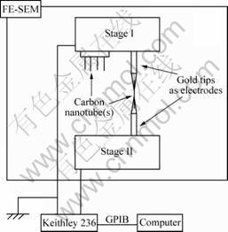
Fig.1 Schematic diagram of nano-manipulator system for electrical property measurement of individual carbon nanotube
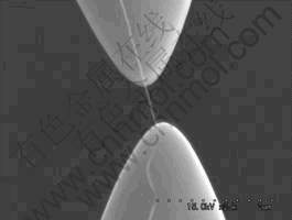
Fig.2 SEM image of individual MWCNT(Both ends of which are fixed on two gold tips (electrodes) of two stages of FE-SEM by the electron beam irradiation for evaluating electrical property of MWCNT)
the carbon nanotube and electrodes, especially in initial measurement cycles.
For electrical measurement of individual MWCNT grown on Pt grid substrate, one carbon nanotube was selected from the carbon nanotube film and attached and fixed on the gold tip by electron beam irradiation on one stage(see Fig.4).
The current-voltage characteristics of the individual multi-walled carbon nanotube are shown in Fig.5. For the first I-V measurement, during increasingly applied voltage up to 4 V, small current flows, which means that this state is highly resistive, which is referable to high resistance state. Then current flows abruptly to 9 ?A at 4.2 V. The state is referable to transition state. Finally, during decreasing voltage, current decreases almost linearly with respect to the applied voltage, which is referable to low resistance state. This figure clearly shows that by increasing the voltage between electrodes, resistance states change from high resistance state (4 M?) to low resistance state (450 k?) via the transition state.
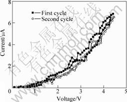
Fig.3 Current-voltage characteristics of individual MWCNT
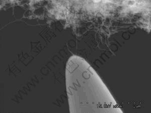
Fig.4 SEM image of individual MWCNT shown in Fig.2 (One end of which is fixed on one gold tip (electrode) of one stage of FE-SEM by the electron beam irradiation for evaluating electrical property of MWCNT)
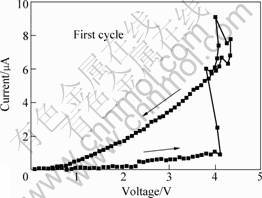
Fig. 5 Current-voltage characteristics of individual MWCNT shown in Fig.4
To investigate the reproducibility of I-V characteristics after transition to low resistance state, the I-V measurement was executed again. I-V characteristics are quite reproducible against voltage increase and decrease. The electrical resistance of single MWCNT is about 450 k�� in linear region under bias voltage from 2 to 4 V. The carbon nanotube can carry large current of up to 6 ��A (current density of about 107 A/cm2) at 4 V, whereas the maximum current densities for normal metals are about 105 A/cm2[16].
The change from high resistance state to low resistance state can be observed in the first measurement cycle due to the imperfect connection between the carbon nanotube and electrodes.
The improvement on the connection between a carbon nanotube and electrodes will be required to get better electrical contact. Better contact can be achived by using low melting point alloy as connector between carbon nanotube and electrode.
4 Conclusions
Aligned carbon nanotube arrays on Fe2O3/SiO2/Si substrate and carbon nanotube film on Pt plate substrates are synthesized using STCVD apparatus at atmospheric pressure by pyrolysis of ethyl alcohol as carbon source, which make it possible to substitute complex apparatus for the growth of carbon nanotubes. This STCVD technique may be potential for large-scale production of MWCNTs. The electrical measurement of individual MWCNT grown on silicon substrate and Pt plate substrate is performed by homemade ��nano-manipulator��, respectively. According to current-voltage curves, the current density that the MWCNT could carry is calculated to be about 107 A/cm2, which is much larger than that of normal metals.
AcknowledgementsThis work is partially supported by Japan Science Promotion Society (JSPS) and New Energy and Industrial Technology Development Organization (NEDO) as a part of Nano-carbon Technology (NCT) project, Japan.
References[1] IIJIMA S. Helical microtubules of graphitic carbon [J]. Nature, 1991, 354: 56-58.
[2] TANS S J,VERSCHUEREN A R M, DEKKER C. Room-temperature transistor based on a single carbon nanotube[J]. Nature, 1998, 393: 49-52.
[3] BACHTOLD A, PETER H, TAKESHI N, DEKKER C. Logic circuits with carbon nanotubes transistor[J]. Science, 2001, 294: 1317-1320.
[4] JAVEY A, WANG Q, URAL A, LI Y, DAI H. Carbon nanotube transistor arrays for multistage complementary logic and ring oscillators[J]. Nano Letters, 2002, 2(9): 929-932.
[5] KONG J, FRANKLIN N R, ZHOU C W, CHAPLINE M G, PENG S, CHO K, DAI H J. Nanotube molecular wires as chemical sensors[J]. Science, 2000, 287: 622-625.
[6] COLLINS P G, BRADLEY K, ISHIGAMI M, ZETTL A. Extreme oxygen sensitivity of electronic properties of carbon nanotubes[J]. Science, 2000, 287: 1801-1804.
[7] MODI A, KORATKAR N, ERIC L, WEI B Q, AJAYAN P M. Miniaturized gas ionization sensors using carbon nanotubes[J]. Nature, 2003, 424: 171-174.
[8] EBBSEN T W, AJAYAN P M. Large-scale synthesis of carbon nanotubes[J]. Nature, 1992, 358: 220-222.
[9] THESS A, LEE R, NIKOLAEV P, DAI H J, PETIT P, ROBERT J, XU C H, LEE Y H, KIM S G, RINZLER A G, COLBERT D T, SCUSERIA G E, TOMONEK D, FISCHER J E, SMALLEY R E. Crystalline ropes of metallic carbon nanotubes[J]. Science, 1996, 273: 483-487.
[10] AMELINCKX S, ZHANG X B. A formation mechanism for catalytically grown helix-shaped graphite nanotubes[J]. Science, 1994, 265: 635-639.
[11] CUMINGS J, MICKELSON W, ZETTL A. Simplified synthesis of double-wall carbon nanotubes[J]. Solid State Commun, 2003, 126: 359-362.
[12] ISHIGAMI M, JOHN C, ZETTL A, CHEN S. A simple method for the continuous production of carbon nanotubes[J]. Chem Phys Lett, 2000, 319: 457-459.
[13] KONG J, CASSELL A M, DAI H J. Chemical vapor deposition of methane for single-walled carbon nanotubes[J]. Chem Phys Lett, 1998, 292: 567-574.
[14] TERRONES M, GROBERT N, OLIVARES J, ZHANG J P, TERRONES H, KORDATOS K, HSU W K, HARE J P, TOWNSEND P D, PRASSIDES K, CHEETHAM A K, KROTO H W, WALTON D R M. Controlled production of aligned-nanotube bundle[J]. Nature, 1997, 388: 52-55.
[15] BOWDEN N B, WECK M, CHOI I S, WHITESIDES G M., Molecule-mimetic chemistry and mesoscale self-assembly[J]. Acc Chem Res, 2001, 34: 231-238.
[16] BAUGHMAN R H, ZAKHIDOV A A, DE HEER W A. Carbon nanotubes��the route toword application[J]. Science, 2002, 297: 787-792.
Foundation item: Project(KM200510772013) supported by the Science and Technology Development Program of Education Committee of Beijing City; Project (2005��2007) supported by the Academic Innovative Team Program (Novel Sensor and Materials: Nanodevice and Nanomaterials) of Education Committee of Beijing City
Corresponding author: ZOU Xiao-ping; Tel: +86-10-64884673-812; Fax: +86-10-64879486; E-mail: xpzou2005@gmail.com


