

Recent progress of CERN RD50 Collaboration
P. LUUKKA
Helsinki Institute of Physics, CERN/EP, CH-1211 Geneva, Switzerland
Received 10 April 2006; accepted 25 April 2006
Abstract:
The objective of the CERN RD50 Collaboration is to develop radiation hard semiconductor detectors for very high luminosity colliders, in particular, for the upgrade of the large hadron collider (LHC) which itself is scheduled to be operational in 2007. The approach of the RD50 has two major research lines, material engineering and device engineering. These are further subdivided into projects covering defect characterization and engineering, new detector materials, detector characterization, new detector structures and full detector systems. Presently, 264 members from 53 institutes are actively participating in the RD50 Collaboration. Detectors made of defect engineered substrates, e.g. high resistivity magnetic Czochralski (MCz-Si), epitaxial silicon (Epi-Si) on Czochralski silicon (Cz-Si) substrate, intentionally thermal donor (TD) compensated p-type MCz-Si and oxygen enriched (DOFZ) silicon, have been demonstrated by the RD50 Collaboration. An overview and highlights of the results of these defect engineering techniques were given in this report.
Key words:
radiation hardness; silicon; particle detector; defect;
1 Introduction
The objective of the CERN RD50 Collaboration is the development of radiation hard semiconductor detectors for very high luminosity colliders, particularly to face the requirements of the proposed upgrade scenario of the LHC to a luminosity of 1035 cm-2?s-1, corresponding to expected total fluencies of fast hadrons above 1016 cm-2 close to the interaction point and reduced bunch-crossing interval of about 10 ns [1]. Presently, 264 members from 53 institutes are actively participating in the RD50 Collaboration. The scientific organization of RD50 is organized into two major research lines, material engineering and device engineering that are further divided into projects covering defect characterization and engineering, new detector materials, detector characterization, new detector structures and full detector systems. Only the specific topics of defect engineering and characterization activities were presented and discussed in this paper. More detailed information can be found in the references [2, 3].
Particle radiation causes irreversible crystallo- graphic defects in the silicon material deteriorating the detector performance. First, the donor doping concentration of silicon is compensated by the dominantly acceptor type defects. This may cause space charge sign inversion (SCSI) in the n-type silicon material, which is followed by the increase of the detector full depletion voltage (Vfd). Second, the leakage current of the detector (Ileak) increases linearly as a function of the accumulated radiation fluence. Third, due to the trapping of charge carriers, the overall charge collection efficiency (CCE) degrades.
The detectors used in the particle tracking systems must be fully depleted at reasonably low operating voltages. A practical limit for the operating voltage is about 500 V. Detectors have traditionally been fabricated on n-type high resistivity silicon wafers made by Float Zone (Fz-Si) crystal growth technique. However, the low oxygen concentration in Fz-Si is a drawback since oxygen has experimentally been found to improve the radiation hardness of the silicon detectors, as demonstrated by the research and development work performed in the framework of CERN RD48 Collaboration[4, 5]. Therefore, the collaboration developed the technique of oxygen-enriched float zone silicon (DOFZ) in which the high oxygen concentration is produced by a long lasting oxidation step (e.g. 72 h at 1 150 ��) performed before the processing of the detector. This results in an average oxygen concentration of 2��1017 cm-3, which is almost one order of magnitude higher than in the standard Fz-Si. Another approach to have high oxygen concentration in the detector is to use Czochralski silicon (Cz-Si), which contains intrinsically high level of oxygen (typically 1017-1018 cm-3), as a substrate material. The Czochralski crystal growth method enables production of silicon wafers with sufficiently high resistivity and with well-controlled oxygen concentration. Although Cz-Si is the basic raw material for microelectronics industry, high resistivity (��1 k��?cm) Cz-Si wafers suitable for detector fabrica- tion have become available only recently [6].
The detectors made of Cz-Si and DOFZ materials have proved to be more radiation hard than the devices made of standard Fz-Si. RD50 is working intensively on the comprehensive characterization of the radiation induced defects that are responsible for the degradation of the macroscopic properties of the particle detectors [5, 6].
2 Shallow donors in oxygen rich detector materials
Shallow donors have twofold influence on the macroscopic properties of the detectors. First, shallow oxygen thermal donors (TD) can be utilized in order to manipulate the effective doping concentration (Neff) of the silicon bulk during the fabrication process [7]. It is important to tailor the full depletion voltage. Second, the shallow donors interact with the radiation defects and influence the radiation hardness of the detectors [8].
It is well known that the aggregation of oxygen atoms leads to the formation of electrically active defects, commonly named thermal donors [9, 10]. The TDs are probably among the most studied defects in the semiconductors. The TDs are shallow donor levels within 0.01-0.2 eV energy range below the conduction band [11]. Their formation strongly depends on the temperature and the oxygen concentration of the silicon material. Heat treatment between 400-600 �� can yield to a TD concentration comparable with the initial doping concentration of the high resistivity material. A quantitative study about the thermal activation of the TDs in high resistivity magnetic Czochralski silicon (MCz-Si) was carried out [12]. TD activation has been performed through an isochronal thermal treatment at 430 �� up to a total time of 120 min. Space charge density after each annealing step was measured by transient charge technique (TCT) [13]. The shallow levels related to the oxygen thermal donors have been observed and studied in detail by thermally stimulated currents (TSC) in the range of 10-70 K [14]. The TSC spectra of the heat-treated and non-heat-treated samples is shown in Fig.1.
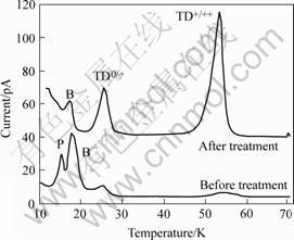
Fig.1 TSC spectra of MCz-Si diodes before and after annealing treatment of 120 min at 430 �� (Reverse bias is Vrev=10 V, heating rate is 0.1 K/s. Deep levels have been filled at lower temperature by 1 min of forward current injection. The reverse bias is applied immediately after the end of the filling time, and the measurements were started after 90 s of de-excitation.)
The evolution of the space charge density caused by the annealing has been unambiguously related to the activation of TDs by the means of current deep level transient spectroscopy (I-DLTS) and TSC analyses. The energy levels and capture cross sections have been evaluated for the single and double TD emissions: TD0/+ (E0/+=75��5 meV, ��0/+=4��10-14 cm2) and TD+/++ (E+/++=170��5 meV, ��+/++=2��10-12 cm2).
Fig.2 shows the TSC spectra of a proton irradiated n-type MCz-Si detector. The irradiation fluence of 24 GeV/c protons is 4��1014 p/cm2 and the sample has been annealed 1 260 min at 60 �� [15].
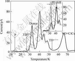
Fig.2 TSC spectra at low temperatures after irradiation with 24 GeV/c protons and dose of 4��1014 cm-2 followed by annealing at 60 �� for 1 260 min
The TSC peak visible at 30 K has been related to a shallow charged defect: the inset shows the occurrence of the Poole Frenkel effect (evidenced by the characteristic shift of the peak temperature as the applied reverse voltage is changed) indicating that the radiation-induced defect should be charged, possibly donor-like. We note that the peaks related to the TD emissions (TD0/+ and TD+/++), observed when the diodes are heated at temperatures of 430 ��, are not present after the irradiation. Similarly, the shallow energy level due to the phosphorus is not observed, probably as a consequence of the formation of the phosphorus-vacancy complex. The same peak, which is related to a defect with energy of around 80 meV [16] has been observed also in the p-type MCz-Si samples after similar irradiation and annealing treatments. For comparison, TSC measure- ments have also been carried out with n-type standard Fz-Si samples after the same irradiation fluence. In Fz-Si samples, this radiation-induced energy level is found with a concentration at least five times lower than in the MCz-Si devices. Moreover, in agreement with the expectations, the VO concentration has been observed to be at least three times lower in Fz-Si than in n-type MCz-Si samples [16]. The observed higher concentra- tions of the VO complex and of the shallow donor at the temperature of 30 K are in agreement with the higher radiation hardness of the MCz-Si devices observed after the proton irradiation with respect to the standard Fz-Si devices. We suggest that the shallow defect, as a donor, is partially compensating the radiation-induced deep acceptors (I defect at 0.54 eV), while the enhanced formation of the VO complex should be related to a partially suppressed I defect formation: the macroscopic effect is to suppress space charge sign inversion, or eventually shift it to higher fluences.
3 Bistable donors (BD)
In addition to oxygen rich silicon materials, MCz-Si and DOFZ, detectors made of epitaxial silicon (Epi-Si) have proved to be very radiation hard in terms of the evolution of the effective doping concentration with respect to the irradiation fluence [17]. 25, 50 and 75 ?m thick epitaxial n-type layers with a nominal resistivity of 50 ??cm were produced using highly doped Cz-Si substrates (0.01 ??cm). During high temperature processing, oxygen diffuses into the epitaxial layer. A SIMS measurement of the oxygen concentration is shown in the reference [17].
The evolution of the Neff with respect to the irradiation fluence for 25, 50 and 75 ?m thick Epi-Si n-type detectors is shown in Fig.3.
From the investigations of the change of the Neff due to irradiation, three main effects attribute to the stable damage. The donor removal reduces the positive space charge by the formation of E-centers (vacancy- phosphorus complex). This component, responsible for the first part of the fluence dependence, is exponentially saturating
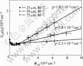
Fig.3 Effective doping concentration, as measured after end of beneficial annealing as function of fluence after 24 GeV/c proton irradiation (Solid lines represent fits according to a model description [9], slope values assigned to the curves represent the donor generation rates.)
due to the exhaustion of the available P-donors. A large value of the doping concentration, as possible in the thin diodes, will delay this exhaustion. For larger fluencies in the Epi-Si diodes the possible creation of the acceptors is obviously always over-compensated by the donors causing an almost linear increase of the Neff in the high fluence range (Feq > 1015 cm-2, as shown Fig.3).
It is however striking that the effect of the stable donor generation is largely depending on the thickness of the device. Indeed, the differences in the Neff(Feq) seen in Fig.3 between 25 ?m (large increase) and 75 ?m diodes (only small increase) are obviously correlated with the oxygen concentration profiles reported in [17]. A direct correlation has to be excluded, because no similar effect was observed in the DOFZ diodes with the same average O-concentration. A first understanding has been provided by the defect spectroscopy investigations, revealing a shallow donor at EC=-0.23 eV, which is not detectable in the Fz-Si diodes[8]. Fig.4 shows the results of TSC- spectra for all of the three n-type Epi-Si diodes.
While the well known point defects like e.g. CiOi, the double vacancy as well as the peak at 115 K, known from previous work with the Fz-Si diodes [18], are measured with the concentrations independent of the diode type and hence independent of the O-concentration, the TSC signal due to the shallow donor (denoted BD) has very similar dependence on the material as the average O-concentration and the stable damage generation (Fig.3).
The following tentative explanation for the generation of the BD donor and hence the radiation tolerance of the n-type Epi-Si diodes has been proposed in the Refs. [8, 19]. A strong similarity of the BD complex to the thermal double donors and the well known fact that the oxygen dimers (O2i) are one of the
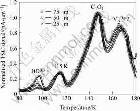
Fig.4 TSC spectra for 25, 50 and 75 ?m n-type Epi-Si diodes after 24 GeV/c proton irradiation with ��eq = 1.8��1014 cm-2 and 120 min annealing at 60 �� (top curve: 25 ?m, bottom one: 75 ?m)
precursors for the formation of the thermal donors [20] leads to the assumption that the dimers are involved in the damage produced BD defects. It is also known that the oxygen dimers have much larger diffusion constant than the oxygen interstitials. Thus it can be expected that they diffuse out from the Cz-Si substrate predominantly after the last high temperature process step thus leading to a larger dimer concentration in the Epi-Si diodes than could be expected from the oxygen concentration alone. Indeed by monitoring the oxygen dimers with measurements of the IO2i concentration, an appreciable enhancement of the relative dimer ratio in n-type Epi-Si diodes with respect to that found in the n-type Cz-Si samples by at least a factor of 2 has been shown. In the standard and oxygen enriched n-type Fz-Si diodes no IO2i defect has been found supporting the general picture [21].
4 Conclusions
Recent developments and advancements of the RD50 collaboration related to the defect engineered silicon have been presented.
The formation of the thermal donors can be utilized to tailor the Vfd of the detectors. Thus, detectors with high oxygen concentration and with low Vfd can be fabricated without additional process complexity or additional high temperature diffusion oxygenation. It is suggested that the shallow defect, as a donor, is partially compensating the radiation-induced deep acceptors yielding to an improved radiation hardness of the MCz-Si devices compared to the standard Fz-Si devices.
It is demonstrated that especially Cz-Si and Epi-Si devices exhibit an unprecedented radiation tolerance. This is mainly due to the high concentration of oxygen as interstitial atoms (Oi) and as so-called oxygen dimers (O2). Defect studies indicate that the high Oi concentration leads to a suppression of deep acceptors, while a high concentration of O2 additionally promotes the formation of the shallow donors resulting in a compensation of the radiation induced negative space charge by the deep acceptors.
References
[1] GIANNOTTI F, et al. hep-ph/02004087. 2002-04.
[2] LINSTROEM G, et al. Radiation hard silicon detectors- developments by the RD48 (ROSE) collaboration [J]. Nuclear Instruments and Methods in Physics Research A, 2001, 466: 308.
[3] RUZIN A, et al. Comparison of radiation damage in silicon induced by proton and neutron irradiation [J]. IEEE Trans Nucl Sci, 1999, 46(5): 1310.
[4] H?RK?NEN J, et al. Processing of microstrip detectors on Czochralski grown high resistivity silicon substrates [J]. Nuclear Instruments and Methods in Physics Research A, 2003, 514: 173-179.
[5] RD50 Status Report 2002/2003, CERN-LHCC-2003-058.
[6] RD50 Status Report 2004, CERN-LHCC-2004-031.
[7] H?RK?NEN J, et al. Proton irradiation results of p+/n-/n+ Cz-Si detectors processed on p-type boron-doped substrates with thermal donor-induced space charge sign inversion [J]. Nuclear Instruments and Methods in Physics Research A, 2005, 552: 43-48.
[8] PINTILIE I, et al. Stable radiation-induced donor generation and its influence on the radiation tolerance of silicon diodes [J]. Nuclear Instruments and Methods in Physics Research A, 2006, 556: 197-208.
[9] OEHRLEIN G S. Silicon-oxygen complexes containing three oxygen atoms as the dominant thermal donor species in heat-treated oxygen-containing silicon [J]. J Appl Phys, 1983, 54: 5453.
[10] WADA K. Unified model for formation kinetics of oxygen thermal donors in silicon [J]. Phys Rev B, 1984, 10: 5884.
[11] OURMAZD A, et al. Oxygen-related thermal donors in silicon: A new structural and kinetic model [J]. J Appl Phys, 1984, 58: 1670.
[12] BRUZZI M, et al. Thermal donors activation via isochronal annealing in magnetic czochralski high resistivity silicon [J]. Journal of Applied Physics. (in press)
[13] EREMIN V, et al. Development of transient current and charge techniques for the measurement of effective net concentration of ionized charges (Neff) in the space charge region of p-n junction detectors [J]. Nucl Instr And Meth, 1996, A372: 188.
[14] BIGGERI U, et al. Studies of deep levels in high resistivity silicon detectors irradiated by high fluence fast neutrons using a thermally stimulated current spectrometer [J]. IEEE Trans Nucl Sci, 1996, 41(4): 964-975.
[15] BRUZZI M, et al. Processing and first characterization of detectors made with high resistivity n- and p-type Czochralski silicon [J]. Nucl Instrum Meth A, 2005, 552: 20-26
[16] SCARINGELLA M, et al. Localized energy levels generated in magnetic Czochralski silicon by proton irradiation and their influence on the sign of the space charge density [J]. Nuclear Instruments and Methods in Physics Research A, Article in press.
[17] LINDSTROEM G, et al. Radiation tolerance of epitaxial silicon detectors at very large proton fluences [J]. Nucl Instrum Meth A, 2006, 556: 451.
[18] MOLL M. University of Hamburg, 1999.
[19] PINTILIE I, et al. Radiation-induced donor generation in epitaxial and Cz diodes [J]. Nucl Instrum Meth, 2005, A552: 56-60.
[20] LEE Y J, et al. First-principles study of migration, restructuring, and dissociation energies of oxygen complexes in silicon [J]. Phys Rev B, 2002, 65: 085205.
[21] STAHL J. University of Hamburg, 2004.
Corresponding author: P. LUUKKA; Tel: +41-22-7678783; Fax: +42-22-7673600; E-mail: panja.luukka@cern.ch.
