

Growth of CuI buffer layer prepared by spraying method
YAN You-hua, LIU Ying-chun, FANG Ling, LU Zhi-chao, LI Zheng-bang, ZHOU Shao-xiong
China Iron and Steel Research Institute Group, Advanced Technology and Materials Co., Ltd., Beijing 100081, China
Received 22 October 2009; accepted 23 February 2010
Abstract:
CuI thin films with nano-scale grains of about 35nm were deposited via spraying method with using acetonitrile as solvent. The influence of iodine doping concentration in acetonitrile solution on the structure, topographic and optical properties of CuI thin films was investigated. X-ray diffraction results showed that CuI iodine-doped films doped CuI?I2 were in ��-phase of zinc blende structure with (111) preferential plane. Scanning electron microscopy revealed that the microstructure of CuI films depended on the relative amount of doping iodine in the solution. When the iodine doping amount in acetonitrile solution was 0.025 g, the film was uniform and compact, the optical transmittance was 75.4% in the part of visible region and the energy band gap was close to 2.96 eV.
Key words:
CuI thin film; buffer layer; spraying method; iodine doping;
1 Introduction
Thin film solar cells based on wide-gap chalcopyrite are promising for the next generations of photovoltaic modules[1]. In recent years, up to 12% power conversion efficiency has been achieved by fabricating Mo/CuInS2/CdS/TCO structure device[2]. Mismatch in the electron affinity and band offset at the junction between CuInS2 and CdS were considered to be one of the major limiting factors towards further increasing the efficiency value[3]. Also, the use of Cd in synthesizing the materials was not favored due to its toxicity. The interest in alternative buffer layers to CdS in CuInS2 (CIS) photovoltaic technology is motivated primarily by the potential to enhance solar cell current generation by the use of materials with wider band-gap than CdS and by a desire for Cd-free cells[4-5]. In comparison with CdS, CuI has several advantages as follows: 1) CuI with a band gap of 3.0 eV may outperform traditional CdS material (Eg=2.4 eV) and transmit higher energy photos; 2) CuI has a better lattice-matching to CuInS2 thin film absorbers than CdS[6]; 3) from the point of environment safety, the establishment of a Cd-free process is significantly desirable in order to eliminate the Cd-containning waste discharged from the chemical-bath deposition (CBD) process[7]. As a simple wide band gap semiconductor, CuI belongs to the I-VII semiconductors with zink blende structure. CuI has three crystalline phases, ��, �� and ��. The low-temperature ��-phase (cubic) behaves as a p-type semiconductor. The uppermost valence bands of CuI (��15, 2 and ��12, 1) are derived from the 3d states of Cu and 5p states of I. The direct fundamental band gap of CuI corresponds to the energy difference of ��15, 2 and ��12, 1 valleys at the �� point in the Brillouin zone and was reported as 3.0 eV[8]. Optimal results were obtained on cells with CuI buffer layer. For large-scale application, CuI was used as a buffer layer on n-CIS absorber in CIS CuT based solar cells manufactured in a roll-to-roll process. A device efficiency of 9.2% was achieved[9]. KONOVALOV[10] studied the material requirements for p-CuI/n-CuInS2 type solar cells and found that this material combination should be rather beneficial for solar cells since there was virtually no valence band offset. VERSCHRAEGEN and BURGELMAN[11] found that the spike height and the spike width in CuI/CuInS2 interface were determined by CuI doping concentration. However, CuI is a relatively new material, its physical properties are still not well-known, and the effects of iodine doping concentration on the microstructure and optical properties of CuI films have not been reported yet.
In this study, the spraying method to fabricate CuI thin films was utilized, and the influence of the iodine doping concentration on structure, topography and optical properties of CuI films was investigated. The film growth mechanism and possibility of using CuI films as the buffer layer of CIS solar cells were also discussed.
2 Experimental
A wide band gap p-type CuI film with a thickness of about 85 nm was obtained by spraying a precursor solution consisting of 0.25 g CuI in 50 mL acetonitrile. In order to study the influence of iodine doping concentration on the morphology, structure and optical property of CuI films, solutions of 0.25 g CuI and 0.005, 0.015, 0.025 and 0.035 g I2 in 50 mL acetonitrile were prepared and sprayed on Cu, glass and CuInS2(CIS) substrates, respectively. That is, 0.25 g CuI was fixed and the n(I2) to n(CuI) values in mixed solution varied from 0.015:0.25 to 0.035:0.25. The preparation of CuInS2 films was reported in Ref.[12]. During the spraying process, the substrate temperature was constant at 110 ��C to accelerate the volatilization of solvent and improve the crystallinity of CuI films.
X-ray diffractometry (XRD) was used to identify the crystalline phases, using a Bruker Discover D8 X-ray diffractometer with CuK�� radiation (��=1.54178?). Phase assignment was done by comparing the corresponding d-spacing with the JCPDS database. Surface morphology of the films was observed on a scanning electron microscope (SEM) at an accelerating voltage of 20 kV. High resolution transmission electron microscopy (HRTEM) images were used to study the structural characteristics of the films. The optical properties of the films were measured at normal incidence in a wavelength range from 300 to 760 nm using a double-beam UV-Vis spectrophotometer.
3 Results and discussion
3.1 Surface morphology
Fig.1 shows the SEM images of CuI films with different iodine doping concentrations on Cu substrate. It is interesting that an addition of a trace amount of iodine significantly influences the shape of the CuI grains. CuI grains with elongated shape are obtained in the absence of iodine. Closely packed spherical CuI grains are obtained in the presence of iodine in CuI coating solution. When n(I2)/n(CuI)=0.025:0.25, the grain sizes apparently increase, and the resulting layer consists of up to 1 ��m
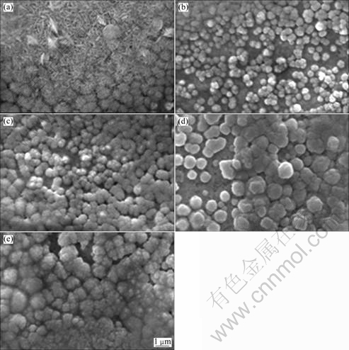
Fig.1 SEM images of CuI thin films with different n(I2)/n(CuI) values: (a) 0:0.25; (b) 0.005:0.25; (c) 0.015:0.25; (d) 0.025: 0.25; (e) 0.035:0.25
aggregates which are known as good charge carrier conducting particles[13].
When iodine doping amount in acetonitrile solution is 0.025 g, the typical HRTEM image is presented in Fig.2. A representative CuI crystal is shown in Fig.2(a), the grain size of which is approximately 35 nm. The corresponding fast Fourier transform (FFT) along the ![]() zone axis (square area in Fig.2(a)) is displayed in the inset of Fig.2(b). Electron diffraction indicates that the plane spacing is 0.348 nm (Fig.2(b)). For CuI film used as the buffer layer deposited on the top of the CuInS2 absorber, the importance lies on whether the plane spacing matches one of the absorber layers. It can be obtained from Fig.2(b) that the plane spacing is the same as that of the chalcopyrite CuInS2, which means that iodine-doped CuI thin films CuI?I2 doped iodine are suitable for fabricating high quality heterojunctions with lattice-matched CuInS2 absorber[11].
zone axis (square area in Fig.2(a)) is displayed in the inset of Fig.2(b). Electron diffraction indicates that the plane spacing is 0.348 nm (Fig.2(b)). For CuI film used as the buffer layer deposited on the top of the CuInS2 absorber, the importance lies on whether the plane spacing matches one of the absorber layers. It can be obtained from Fig.2(b) that the plane spacing is the same as that of the chalcopyrite CuInS2, which means that iodine-doped CuI thin films CuI?I2 doped iodine are suitable for fabricating high quality heterojunctions with lattice-matched CuInS2 absorber[11].

Fig.2 TEM image (a) and electric refraction pattern (b) of CuI grain for n(I2)/n(CuI)=0.025:0.25
3.2 Structural properties
Fig.3 shows the X-ray diffraction patterns of CuI thin film with different iodine doping concentrations. It can be seen that CuI films doped iodine exhibit a preferential orientation along (111) plane, which corresponds to ��-phase with a zinc blende face centered cubic structure. It is worthy to note that the intensity of CuI (111) reflection peak in Fig.3(c) apparently becomes sharpest and strongest, which indicates that the crystallinity of CuI film is improved when the iodine doping amount increases to 0.025 g. An average value of the crystallite size at (111) plane can be also obtained by applying Scherrer��s formula[14]. The average diameter of CuI crystallite is 32 nm when n(I2)/n(CuI)= 0.025:0.25, which is in accordance with the result in Fig.2(a).

Fig.3 XRD patterns of CuI thin films with different n(I2)/n(CuI) values: (a) 0:0.25; (b) 0.005:0.25; (c) 0.015:0.25; (d) 0.025:0.25; (e) 0.035:0.25
3.3 Optical characteristics
Fig.4 shows the optical transmittance spectra of CuI thin films with different iodine doping concentrations. The transmittance measurements at room temperature show that CuI films with or without iodine doping have an average transmittance as high as 65% in a wavelength range larger than 513 nm, which is comparable to that of the ZnS films deposited from acetate solution[15]. In Fig.4, it is found that the maximum transmittance in the visible regions is 75.4% when the iodine amount in acetonitrile solution is 0.025 g, which is close to the transmission of 75% obtained by SANKAPAL et al[16].

Fig.4 Optical transmittance spectra of CuI thin films with different n(I2)/n(CuI) values
Fig.5 shows the square of absorption coefficients �� versus the photon energy (h��) for the CuI films as a function of the iodine doping concentration. �� can be evaluated from the measurements of optical transmittance (T) and film thickness (d) as
��=-ln(T)/d (1)
The optical band gap Eg is related to the absorption coefficient �� according to
��h��=A(h��-Eg)n (2)
where A is a constant; h is the Plank constant; and n=1/2 for direct gap material. It is now well established that CuI is a direct gap semiconductor, so the optical band gap Eg can be obtained by extrapolating the linear portion of the plot (h�ͦ�)2 versus h�� to ��=0, which is illustrated in Fig.5. Linear nature of the plots indicates that the CuI is direction bandgap material. The extrapolation of the liner parts of the curves to energy axis gives the direct bandgap ��Eg�� value as 2.96 eV for n(I2)/n(CuI)=0.025:0.25, which is in good agreement with the value of 2.97 eV reported by other workers[16], as shown in the inset of Fig.5. It can be seen that the optical absorption edges of all films are very steep, which implies that CuI films have a good homogeneity in the shape and size of the grains.

Fig.5 Square of absorption coefficients ��2 vs photon energy for CuI films with different n(I2)/n(CuI) values: 1��0:0.25; 2��0.005:0.25; 3��0.015:0.25; 4��0.025:0.25; 5��0.035:0.25
3.4 CIS/CuI microstructure
Fig.6 shows the SEM image and XRD pattern of CuI thin films deposited on CIS film when n(I2)/n(CuI)=0.025:0.25. From Fig.6 (a), it can be seen that a better surface coverage is observed on CuInS2 surface. Fig. 6(b) shows X-ray diffraction pattern of CuI films deposited on CIS. The XRD diffraction peaks correspond to (112), (103), (200), (204) and (312) reflection lines of CIS phase, (111) and (220) reflection lines of CuI phase, (111) and (200) reflection lines of copper phase, and the diffraction peak of the copper phase originates from Cu substrate. CuInS2 chalcopyrite structure is confirmed by the presence of the characteristic peaks of chalcopyrite (103)[17]. It is obvious that the CIS film has a single-phase chalcopyrite structure with (112) preferred plane. Preferential orientation of CuI film is observed along (111) plane which is in accordance with ��-phase with a zinc blend structure faced centered cubic structure. The (111) preferred plane in CuI films is beneficial for good lattice matching with CIS (112) for efficient device fabrication[18]. CuI is suitable for using as the buffer layer of thin film solar cells with CuInS2 absorber layer by replacing CdS.

Fig.6 SEM image (a) and XRD pattern (b) of CuI thin films with n(I2)/n(CuI)=0.025:0.25 deposited on CIS film
4 Conclusions
1) CuI films doped iodine exhibit a preferential orientation along (111) plane, which corresponds to ��-phase with a zinc blende face centered cubic structure. This is beneficial for good lattice matching with CIS (112) for efficient device fabrication.
2) The microstructure and optical property largely depend on the relative iodine doping concentration in acetonitrile solution. When n(I2)/n(CuI)=0.025:0.25, CuI film consists of up to 800 nm-aggregates formed by 35 nm-particles, the d(HKL) spacing is 0.348 nm, the maximum transmittance in the visible regions is 75.4% and the energy band gap is close to 2.96 eV.
3) CuI is suitable for using as the buffer layer of the CuInS2 solar cells by replacing CdS. It will lead to an expectation that a high conversion efficiency, low cost and environment pollution-free technique can be developed.
References
[1] MEYER N, MEEDER A, SCHMID D. Pilot production of large-area CuInS2-based solar modules [J]. Thin Solid Films, 2007, 515(15): 5979-5984.
[2] CONNOR S T, HSU CH M, WEIL B D, ALONI S, CUI Y. Phase transformation of biphasic Cu2S-CuInS2 to monophasic CuInS2 nanorods [J]. Journal of the American Chemical Society, 2009, 131(13): 4962-4966.
[3] BADYOPADHYAYA S, CHAUDHURI S, PAL A K. Synthesis of CuInS2 films by sulfurization of Cu/In stacked elemental layers [J]. Solar Energy Materials & Solar Cells, 2000, 60(4): 323-339.
[4] MALM U, MALMSTR?M J, PLATZER-BJ?RKMAN C, STOLT L. Determination of dominant recombination paths in Cu(In,Ga)Se2 thin-film solar cells with ALD-ZnO buffer layers[J]. Thin Solid Films, 2005, 480-481: 208-212.
[5] RABEH M B, CHAGLABOU N, KANZARI M. Structural, optical and electrical properties of annealed Sb-doped CuInS2 thin films grown by thermal evaporation method [J]. Chalcogenide Letters, 2009, 6(2): 83-89.
[6] SPIERING S, HARISKOS D, POWALLA M, NAGHAVI N, LINCOT D. Cd-free Cu(In,Ga)Se2 thin-film solar modules with In2S3 buffer layer by ALCVD [J]. Thin Solid Films, 2003, 431-432: 359-363.
[7] HARISKOS D, SPIERING S, POWALLA M. Buffer layers in Cu(In, Ga)Se2 solar cells and modules [J]. Thin Solid Films, 2005, 480-481: 99-109.
[8] SIRIMANNE P M, RUSOP M, SHIRATA T, SOGA T, JIMBO T. Characterization of CuI thin films prepared by different techniques [J]. Materials Chemistry and Physics, 2003, 80(2): 461-465.
[9] WINKLER M, GRIESCHE J, KONOVALOV I, PENNDORF J, WIENKE J, TOBER O. CIS CuT-solar cells and modules on the basis of CuInS2 on Cu-tape [J]. Solar Energy, 2004, 77(6): 705-716.
[10] KONOVALOV I. Material requirements for CIS solar cells [J]. Thin Solid Films, 2004, 451-452: 413-419.
[11] VERSCHRAEGEN J, BURGELMAN M. Numerical modeling of intra-band tunneling for hetero-junction solar cells in SCAPS[J]. Thin Solid Films, 2007, 515(15): 6276-6279.
[12] YAN You-hua, LIU Ying-chun, FANG Ling, ZHU Jing-sen, ZHAO Hai-hua, LI De-ren, LU Zhi-chao, ZHOU Shao-xiong. Characterization of CuInS2 thin films prepared by sulfurization of Cu-In precursor [J]. Transactions of Nonferrous Metals Society of China, 2008, 18(5): 1083-1088.
[13] STAKHIRA P Y, CHERPAK V V. The properties of heterojunction based on CuI/pentacene/Al [J]. Thin Solid Films, 2009, 83(8): 1129-1131.
[14] SANKAPAL B R, ENNAOUI, GUMINSKAVA T, DITTRICH T H, BOHNE W, R?HRICH J, STRUB E, LUX-STEINER M C H. Characterization of p-CuI prepared by the SILAR technique on Cu-tape/n-CuInS2 for solar cells[J]. Thin Solid Films, 2005, 480-481: 142-146.
[15] MURALI K R, KUMARESAN S. Characteristics of brush plated ZnS films [J]. Chalcogenide Letters, 2009, 6(1): 17-22.
[16] SANKAPAL B R, GONCALVES E, ENNAOUI A, LUX-STEINER M CH. Wide band gap p-type windows by CBD and SILAR methods[J]. Thin Solid Film, 2004, 451-452: 128-132.
[17] BRINI R, KANZARI M, REZIG B, WERCKMANN J. Effect of annealing on properties of CuInS2 thin films [J]. J Appl Phys, 2005, 30(3): 153-158.
[18] DEGRAVE S, BURGELMAN, NOLLET P. Quantitative study of solar cells based on Cu-In-S based absorber layers grown by the CISCuT-process [J]. Opto-Electronics Review, 2000, 8(4): 295-298.
��Ϳ���Ʊ������CuI��Ĥ������
���л�, ��ӭ��, �� ��, ¬־��, ������, ������
�����о���Ժ ��̩�Ƽ��ɷ�����˾������100081
ժ Ҫ����������Ϊ�ܼ�����Ϳ�����Ʊ������ߴ�ԼΪ35 nm��CuI��Ĥ���о�������Һ�е����Ũ�ȶ�CuI��Ĥ�ṹ����ò��ѧ���ܵ�Ӱ�졣XRD����������������ӵ�CuI��Ĥ���Ц�̬������п��ṹ����(111)��������ȡ��������SEM�����ʾCuI��Ĥ���ṹ��������Һ�е�������йأ���������Һ�в��ӵ�Ϊ0.025 gʱ�����Ʊ���CuI��Ĥ���ȡ����ܣ��ڿɼ��������ѧ���ʿɴ�75.4%���������Ƚӽ�2.96 eV��
�ؼ��ʣ�CuI��Ĥ������㣻��Ϳ���������
(Edited by FANG Jing-hua)
Foundation item: Project (2091003) supported by Beijing Natural Science Foundation, China
Corresponding author: YAN You-hua; Tel: +86-10-58742809; E-mail: yanyouhua@atmcn.com
DOI: 10.1016/S1003-6326(11)60722-X
