

Synthesis of single crystalline CdS nanowires with polyethylene glycol 400 as inducing template
XU Guo-yue(���Ծ), WANG Han(�� ��), CHENG Chuan-wei(�̴�ΰ),
ZHANG Hai-qian(�ź�ǭ), CAO Jie-ming(�ܽ���), JI Guang-bin(�����)
Nanomaterials Research Institute, College of Materials Science and Technology,
Nanjing University of Aeronautics and Astronautics, Nanjing 210016, China
Received 8 May 2005; accepted 9 September 2005
Abstract:
Solvothermal technique, an one-step soft solution-processing route was successfully employed to synthesize single crystalline CdS nanowires in ethylenediamine medium at lower temperature (170 ��) for 1��8 d. In this route, polyethylene glycol 400 (PEG400) was used as surfactant, which played a crucial role in preferentially oriented growth of semiconductor nanowires. Characterizations of as-prepared CdS nanowires by X-ray powder diffraction(XRD), transmission electron microscopy(TEM) indicate that the naonowires, with typical diameters of 20nm and lengths up to several micrometers, have preferential [001] orientation. Also, investigations into the physical properties of the CdS nanowires were conducted with UV-Vis absorption spectroscopy and photoluminescence emission spectroscopy. The excitonic photo-optical phenomena of the nanowires shows the potential in the practical applications.
Keywords: ��-��semiconductor; cadmium sulfide; nanowires; single crystal; photoluminescence properties
1 Introduction
Nanostructured materials are of much current interest for extensive potential application in electronics, optics, catalysis, ceramics, magnetic storage and mechanical devices or in mesoscopic physics[1��3]. In all these nanoscale materials, one- dimensional semiconductors such as nanowires(NWs) and nanorods(NRs), have demonstrated significant potential as fundamental building blocks for assembling a range of nanoelectronic and nano- photonic device[4��6] including room-temperature field-effect transistor(FETs)[7, 8], p-n diodes[8, 9], bipolar junction transistor, and recently, complemen- tary inverter[9] which represents a key component for logic. HU et al[10] also presented substantial promise for fabricating integrated nanosystems. CdS, as a typical wide band-gap��-��semiconductor, has a band-gap of 2.42 eV at room temperature. It has many commercial or potential applications in light-emitting diodes, solar cell, or other optoelectronic devices. The synthesis and study of CdS nanowires and nanorods have stimulated much research and technological interest[11��14]. QIAN��s group developed a new chemical technique called solvothermal method to synthesize CdS nanowires and nanorods[15��18]. In this communication, we modified the above route and used a different polymer as the inducing template. As compared with the templates used in QIAN��s experiments, ours has obvious advantages as follows: 1) PEG400 has thermal stability and unhydrolyzation properties, which makes it more environmentally friendly. In addition, PEG400 is more common, which could reduce the cost of experiments and simplify the experiments process; 2) PEG-400 can be easily separated from the products only by deioned water and absolute alcohol washing, so it is able to obtain high purity single crystalline CdS nanowires; 3) The obtained CdS nanowires have much smaller diameters, which is very important to the mesoscopic properties and fabrication of nanodevices[19]. Using cadmium nitrate and thiourea as starting material, we have successfully synthesized the well-dispersed single crystalline CdS nanowires with typical diameters of 20 nm and lengths up to several micrometers.
2 Experimental
2.1 Chemical reagent and reactors
All the chemicals used in this route were reagent grade without further purification. Cd(NO3)2��4H2O and thiourea were provided as Cd and S source, respectively. Polyethylene glycol 400 (PEG400) was used as the inducing soft template during the synthesis process. The bidentate ligand ethylenediamine often used in solvothermal synthesis under supercritical conditions was chosen as the reaction medium. Commercial Teflon-lined stainless-steel autoclaves of 50 mL capacity were used as the reactor.
2.2 Synthesis procedure
0.001 mol Cd(NO3)2��4H2O was dissolved into 15.0 g polyethylene glycol 400 gel (PEG400, 5.0 g; deionized water, 10.0 g), kept at room temperature for 24 h in order to achieve good dispersion of Cd2+ in the polymer matrix. 0.001mol thiourea was dissolved in 25 mL ethylenediamine, and then the PEG gel dosed with Cd2+ was mixed with the ethylenediamine solvent. The mixture was put into the Teflon-lined stainless-steel autoclave of 50 mL capacity. The tank was maintained at 170 �� for 1��8 d and allowed to cool down to room temperature. The yellow products obtained were washed with absolute alcohol and deionized water for several times. The sample was dried in vacuum at 60 �� for 4��5 h.
2.3 Characterization
The products obtained were characterized by X-ray powder diffraction(XRD) patterns employing a scanning rate of 0.02(��)/s in the 2�� range from 10��to 80��, using a Bruker D8 Advance diffracto- meter equipped with graphite monochromatized Cu K�� radiation (��=1.540 5 ?) operated at 40 mA and 40 kV. Transmission electron microscopy (TEM) and selected-area electron diffraction(SAED) observations were conducted on a JEM-200CX transmission electron microscope, using an accelerating voltage of 200 kV. The sample was dissolved in acetone and dispersed to suspension by an ultrasonic disperser. Room-temperature UV-Vis measurement was made with a HP-6100 UV-Vis scanning spectrophotometer in 300��600 nm wavelength range using 1cm quartz cuvettes. The photoluminescence emission(PL) spec- trum was taken at room temperature with a Hitachi 850 Spectrofluorophotometer.
3 Results and discussion
3.1 XRD measurements
XRD patterns of the products obtained at different reaction times are shown in Fig.1. In Fig.1, the curves from (a) to (d) represent the products prepared in varied reaction times: 1, 2, 4 and 8 d, respectively. All the peaks could be indexed as a typical hexagonal phase (wurtzite structure) CdS. The calculated cons- tants a=4.136 ? and c=6.713 ? are well consistent with the reported data for CdS (JSPDS Card File No.06-0314). All the curves in Fig.1 show that the (002) peak is comparatively sharper than that of the other peaks and has preferential [001] orientation, which indicates these CdS nano- crystallities grow along this direction.
3.2 Effects of reaction time on synthesis of CdS nanowires
Fig.1 shows the XRD patterns of the products obtained in varied reaction times from 1 d to 8 d. It can be seen in Fig.1 that as the reaction time is prolonged from 1 d to 4 d, the (100) and (101) peaks almost keep unchanged, while the (002) peak becomes sharper and sharper. This result indicates that when the reaction time is prolonged, the CdS nanocrystallities mostly grow along the [001] orientation rather than other directions. That is, when the reaction time is prolonged, the CdS nanowires would grow longer and longer along the [001] orientation with diameter remaining nearly unchanged. It also can be seen from the patterns when the reaction time is further prolonged above 4 d, the nanowires grow little or stop growing. This result is consistent with those by TEM and SAED observations, which we will discuss later.
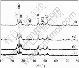
Fig.1 XRD patterns of CdS nanowires prepared at different reaction times by present route: (a) 1 d; (b)2 d; (c) 4 d; (d) 8 d
3.3 TEM and SAED observations
TEM images for the samples obtained for different reaction times (1��4 d) at 170 �� are shown in Fig.2. Fig.2 shows that all the CdS nanocrystallities are homogeneous nanowires or nanorods with uniform diameters of about 20 nm and lengths up to several micrometers. In addition, it can be seen from Fig.2 that the length of CdS nanowires grows longer and longer, which indicates the aspect ratio of the as-prepared CdS nanowires is becoming higher and higher. The TEM observation is consistent with the result by XRD analysis. The as-prepared CdS nanowires may aggregate together sometimes, but the well-dispersed single crystalline nanowires can be easily found by TEM everywhere. Fig.3(a) shows a typical single crystalline CdS nanowire for the sample obtained in 4 d, and it has a smooth and straight morphology. The selected area electron diffraction pattern(SAED) (Fig.3(b)) reveals the single crystalline nature of the as-prepared CdS nanowires, which can be indexed to the strong reflection of wurtzite CdS [001].
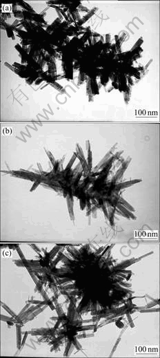
Fig.2 TEM images of CdS nanowires prepared by present route for different reaction times at 170 ��: (a) 1 d; (b) 2 d; (c) 4 d
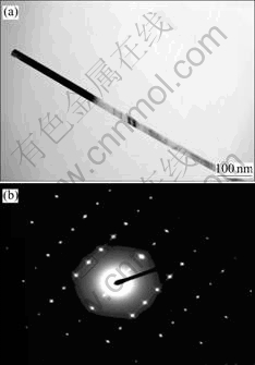
Fig.3 TEM images of typical CdS nanowire(a) and selected- area electron diffraction pattern of wurtzite CdS nanowire(b)
3.4 UV-Vis absorption spectroscopy and photo- luminescence(PL) spectrum
The optical properties of the CdS nanowires are both attractable and remarkable. The UV-vis absorption and photoluminescence(PL) spectrum of CdS nanowires are very complex and their explanation has attracted some controversies.
The UV-Vis absorption spectrum for the CdS nanowires obtained for 4 d is shown in Fig.4. The sample was dispersed in absolute ethanol by ultrasonic disperser. The curve shows an obvious peak at 500 nm. It was reported that only the presence of a narrow cluster size distribution may cause the presence of this spectrum feature[20, 21]. The absorption edge for the bulk hexagonal CdS is at 512 nm(2.42 eV). Compared with the bulk CdS, it is believed that the blue shift in absorption peak was obviously caused by the quantum confinement effect.
Fig.5 shows the photoluminescence(PL) emission spectrum of an absolute ethanol solution containing CdS nanowires that is obtained by present route for 4 d. The pattern consists of one strong and narrow emission at 340 nm using a 310 nm excitation wavelength. The luminescence at 340 nm may be attributed to a higher level transition in CdS crystallites. It was reported that this kind of band-edge luminescence is caused by the recombination of excitons and/or shallowly trapped electron-hole pairs[21]. The apparent blue shift and the strong peak are also indicatives of the size quantization of as-prepared CdS nanowires.
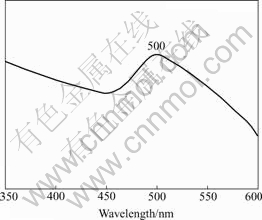
Fig.4 UV-Vis absorption spectrum of CdS nanowires obtained by present route for 4 d
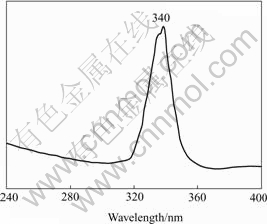
Fig.5 Photoluminescence emission (��ex =310 nm) spectrum of CdS nanowires
A possible mechanism for the formation of the CdS nanowires was presented[15��18]. In our synthetic system, the investigations into CdS nanowire formation indicated that the nucleation and growth were well controlled. Firstly, ethylenediamine(en), as a strongly bidentating solvent, was ready to form relatively stable Cd2+ complexes(log��2 =10.09). Next, the thiourea was inclined to decompose at such a high temperature(170 ��) and generate S2�� ions slowly and homogeneously. The S2�� ions will react with the Cd2+ ions that has chelated with ethylenediamine in a reversible and effective pathway. The overall reaction process could be illustrated by Eqns.(1)[22] and (2):
![]() (1)
(1)
![]() (2)
(2)
Notablely, the polyethylene glycol 400 plays an important role in one-dimensional growth of CdS crystallites, in the absence of which only short nanorods can be obtained[23]. Cd2+ ions were well dispersed in the polymer matrix.The polymer may connected with the ethylenediamine to form chain structures with many pores. These pores are connected and continuous. So in the process of the CdS formation, PEG-400 gel served as a molecular template in control of the CdS crystal growth. At the early stage,only small nanocrystals form, with prolonged duration, these small nanocrystals evolve into long nanowires along the polymer chains. The time effects in the nanowires growth were proved by XRD and TEM analyses. Comparatively, the simple electrochemical deposition into anodic alumina only gets short CdS nanorods or nanoparticles with wide distribution of lengths and widths, moreover the CdS nanorods are polycrystalline[24]. The same solvothermal method, which uses polyacrylamide(PAA) as inducing template, results in much thicker widths (about 40 nm) of the CdS nanowires, causing a relative low aspect ratio[17, 18].
4 Conclusions
Single crystalline CdS nanowires with straight and smooth morphology have been successfully synthesized by treatment of Cd2+ well dispersed in PEG400 gel with thiourea in ethylenediamine medium at 170 �� for several days. The CdS nanowires obtained are single crystalline nature and continuous. Significantly, the length of the CdS nanowires can be controlled by regulating the reaction time. These continuous single crystalline CdS nanowires may have many applications in optoelectronic devices, which are under process in our future work.
Acknowledgement
We thank Professor HONG Jian-ming of Nanjing University for use of the TEM and PL measurements.
References
[1] Alivisatos a p. Semiconductor clusters, nanocrystals, and quantum dots[J]. Science, 1996, 271: 933��937.
[2] Wang y, Herron n. Nanometer-sized semiconductor clusters: materials synthesis, quantum size effects, and photophysical properties[J]. J Phys Chem, 1991, 95(2): 525��532.
[3] Calvert p. Nanotube composites��a recipe for strength[J]. Nature, 1999, 399(6733): 210��211.
[4] Fasol g. Room-temperature blue gallium nitride laser diode[J]. Science, 1996, 272: 1751��1752.
[5] Stafford a, Baeriswyl d, B��rki j. Jellium model of metallic nanocohesion[J]. Phys Rev Lett, 1997, 79: 2863��2866.
[6] H?ppleer c, Zwerger w. Quantum fluctuations in the cohesive force of metallic nanowires[J]. Phys Rev B, 1999, 59: R7849��R7851.
[7] Cui y, Duan x, Hu j, LIEBER C M. Doping and electrical transport in silicon nanowires[J]. J Phys Chem B, 2000, 104(22): 5213��5216.
[8] Duan x, Huang y, Cui y, WANG J F, LIEBER C M. Indium phosphide nanowires as building blocks for nanoscale electronic and optoelectronic devices[J]. Nature, 2001, 409(6816): 66��69.
[9] Cui y, Lieber c m. Functional nanoscale electronic devices assembled using silicon nanowire building blocks[J]. Science, 2001, 291: 851��853.
[10] Hu j, Odom t w, Lieber c m. Chemistry and physics in one dimension: synthesis and properties of nanowires and nanotubes[J]. Acc Chem Res, 1999, 32: 435��445.
[11] Li y, Xu d, Zhang q, CHEN D, HUANG F, XU Y, GUO G, GU Z. Preparation of cadmium sulfide nanowire arrays in anodic aluminum oxide templates[J]. Chem Mater, 1999, 11(12): 3433��3435.
[12] Duan x, Lieber c m.General synthesis of compound semiconductor nanowires[J]. Adv Mater, 2000, 12(4): 298��302.
[13] ZHANG Peng, GAO Lian. Synthesis and characterization of CdS nanorods via hydrothermal microemulsion[J]. Langmuir, 2003, 19(1): 208��210.
[14] SHAO Ming-wang, XU Fen, PENG Yi-ya, WU J, LI Qing. Microwave-templated synthesis of CdS nanotubes in aqueous solution at room temperature[J]. New J Chem, 2002, 26(10): 1440��1442.
[15] WU Ji, JIANG Yang, LI Qing, LIU Xiao-ming, QIAN Yi-tai. Using thiosemicarbazide as starting material to synthesize CdS crystalline nanowhiskers via solvothermal route[J]. J Crystal Growth, 2002, 235: 421��424.
[16] YANG Jian, ZENG Jing-hui, YU Shu-hong, YANG L, ZHOU G E, QIAN Y T. Formation process of CdS nanorods via solvothermal route[J]. Chem Mater, 2000, 12(11): 3259��3263.
[17] ZHAN Jin-hua, YANG Xiao-guang, WANG Dun-wei. Polymer-controled growth of CdS nanowires[J]. Adv Mater, 2000, 12(18): 1348��1350.
[18] ZHAN J H, Yang x g, Li s d, WANG D W, XUE Y, QIAN Y T. A chemical solution transport mechanism for one-dimensional growth of CdS nanowires[J]. J Grystal Growth, 2000, 220: 231��234.
[19] Pan z w, Xie s s, Chang b h, WANG C Y, LU Y, LIU W, ZHOU W Y, LI W Z, QIAN L X. Very long carbon nanotubes[J]. Nature, 1998, 394(6694): 631��632.
[20] Modes s, Lianos p. Wavelength dependence of the photochemistry of hydrogen iodide-acetylene complexes in solid krypton[J]. J Phys Chem, 1989, 93: 5834.
[21] Sapanhel l, Anderson m a. Synthesis of porous quantum-size cadmium sulfide membranes: photoluminescence phase shift and demodulation measurements[J]. J Am Chem Soc, 1990, 112(6): 2278��2284.
[22] Yu s h, Yoshimura m, Maria j, CALDERON M, FUJIWARA T, FUJINO T, TERANISHI R. In situ fabrication and optical properties of a novel polystyrene/semiconductor nanocomposite embedded with CdS nanowires by a soft solution processing route[J] . Langmuir, 2001, 17(5): 1700��1707.
[23] LI Ya-dong, LIAO Hong-wei, DING Yi, QIAN Yi-tai, LI Yang, CUI En-zhou. Nonaqueous synthesis of CdS nanorod semiconductor[J]. Chem Mater, 1998, 10(9): 2301��2303.
[24] Routkevitch d, Bigioni t, Moskovits m, et al. Electrochemical fabrication of CdS nanowire arrays in porous anodic aluminum oxide templates[J]. J Phys Chem,1996, 100(33): 14037��14047.
Foundation item: Project(J1300A002) supported by the National Defense Fundamental Fund of China; Project(51410040305hk0214) supported by the Weaponry Equipment Pre-research Foundation of China; Project(90505008) supported by the National Natural Science Foundation of China
Corresponding author: XU Guo-yue; Tel: +86-25-84894320; Fax: +86-25-84892951; E-mail: xuguoy@nuaa.edu.cn
(Edited by LI Xiang-qun)
