

Effect of diode-laser parameters on shear force of micro-joints soldered with Sn-Ag-Cu lead-free solder on Au/Ni/Cu pad
WANG Jian-xin(������)1, XUE Song-bai(Ѧ�ɰ�)1, FANG Dian-song(������)2,
JU Jin-long(�Ͻ���)3, HAN Zong-jie(���ڽ�)1, YAO Li-hua(Ҧ����)1
1. College of Materials Science and Technology, Nanjing University of Aeronautics and Astronautics,
Nanjing 210016, China;
2. College of Economics and Management, Nanjing University of Aeronautics and Astronautics,
Nanjing 210016, China;
3. College of Automation Engineering, Nanjing University of Aeronautics and Astronautics,
Nanjing 210016, China
Received 12 March 2006; accepted 22 August 2006
Abstract:
Soldering experiments with Sn-3.5Ag-0.5Cu lead-free solder on Au/Ni/Cu pad were carried out by means of diode-laser and IR reflow soldering methods respectively. The influence of different heating methods as well as output power of diode-laser on shear force of micro-joints was studied and the relationship between the shear force and microstructures of micro-joints was analyzed. The results indicate that the formation of intermetallic compound Ag3Sn is the key factor to affect the shear force and the fine eutectic network structures of micro-joints as well as the dispersion morphology of fine compound Ag3Sn, in which eutectic network band is responsible for the improvement of the shear force of micro-joints soldered with Sn-Ag-Cu lead-free solder. With the increases of output power of diode-laser, the shear force and the microstructures change obviously. The eutectic network structures of micro-joints soldered with diode-laser soldering method are more homogeneous and the grains of Ag3Sn compounds are finer in the range of near optimal output power than those soldered with IR reflow soldering method, so the shear force is also higher than that using IR reflow soldering method. When the output power value of diode-laser is about 41.0 W, the shear force exhibits the highest value that is 70% higher than that using IR reflow soldering method.
Key words:
diode-laser soldering; Sn-Ag-Cu lead-free solder; shear force; microstructure;
1 Introduction
With low cost, Sn-Pb alloy has been widely used in electronic packaging on account of its low melting temperature and good wettability on substrates, such as Cu and Au/Ni/Cu pads. However, Pb and its compounds in the Sn-Pb solder are harmful to people��s health and the environment, and recent concerns over the toxicity of Sn-Pb solder alloy result in the development of new lead-free solder alloys for electronic packaging[1,2]. Among several lead-free candidate alloys, which have been researched and developed, the Sn-Ag-Cu alloy family is believed to be the best choice[2-4]. Compared with conventional Sn-Pb solder, Sn-Ag-Cu solders exhibit superior tensile and creep properties[5,6], good compatibility with current components[7], and the melting point of eutectic Sn-Ag-Cu solder alloy is lower than that of Sn-Ag alloys and Sn-Cu alloys[8]. Although Sn-Ag-Cu solders are an attractive alternative to eutectic Sn-Pb among all the candidates, more studies are required to investigate their material characteristics in terms of melting point, solderability, mechanical properties, creep resistance, thermal fatigue resistance, and so on[6].
At present, infrared(IR) reflow soldering, convection reflow soldering, and hot plate reflow soldering are the main techniques widely used in electronic packaging, but the high packaging density of components on printed circuit boards, and the subsequent reduction in size continue to pose great challenges to these entire heating methods. Defects such as bridging tend to exist using these techniques mentioned above. On the other hand, if solder, whole component and whole substrate are in the same soldering temperature, stress and strain will highly concentrate in thermal cycles under the subsequent service conditions as a result of different coefficients of thermal expansion, so the micro-joint is usually easy to fail[9].
With the development of lasers, laser soldering is more and more widely used in the electronic fields[10]. Laser soldering enables the delivery of a large amount of energy to specific locations, even the place difficult to reach. The energy is absorbed by the solder in a short time, making the solder melt and spread around the lead, without causing heat-related damage to surrounding areas or components. Once the laser beam removes, the solder solidifies rapidly to form the required micro-joint. Actually, the laser soldering process brings several advantages mainly in terms of localized heating, rapid rise and fall in temperature, noncontact and easy automation. These features make laser soldering especially be applicable for special substrates, thermal sensitive components, and high-temperature and lead-free solders[11,12].
A number of different lasers have been used for soldering, while it has been found[12,13] that semiconductor diode laser is advantageous due to the fact that the energy produced is efficiently absorbed by the solder, but less absorbed by the substrate. In addition, because of small size and low mass, which leads to low cost, diode laser gains high interest as a pump source for electronic packaging[12].
In this study, soldering experiments with Sn-3.5Ag-0.5Cu lead-free solder on Au/Ni/Cu pad were carried out by means of diode-laser and IR reflow soldering methods respectively. The influence of different heating methods as well as output power of diode-laser on shear force of micro-joints was studied, and the relationship between shear force and microstructures of micro-joints was analyzed.
2 Experimental
The 0805 rectangular chip component was chosen in the experiment. The solder adopted in the experiment was Sn-3.5Ag-0.5Cu, and its melting point is about 217��. The printed circuit board(PCB) was selected with Au/Ni/Cu pad structure. Rectangular chip components were soldered on Au/Ni/Cu pad by means of diode-laser and IR reflow soldering methods respectively. Fig.1 shows the schematic diagram of LY-FCDL-WS90 diode-laser soldering system. The shear force of micro-joints was tested by STR-1000 joint strength tester made in Japan. Finally, MM6 optical microscope was used to observe the microstructures of micro-joints.
One of the most important advantages of laser soldering is its ability to set process parameters to suit the requirements of individual solder joint. The property of micro-joint mainly depends on the diode-laser parameters such as the output power of diode-laser (P) and the soldering speed[12]. The solder does not spread sufficiently with low output power, and excesses output power results in the thermal breakdown of the printed circuit board, therefore, different output power values (34.1, 37.5, 41.0, 44.5 and 48.8 W) were adopted based on the former experimental results. Effect of the output power of diode-laser on shear force of micro-joints soldered with Sn-Ag-Cu lead-free solder on Au/Ni/Cu pad was studied.

Fig.1 Schematic diagram of diode-laser soldering system
3 Results and discussion
3.1 Results of shear force test
After rectangular chip components were soldered, the shear forces of micro-joints soldered under different techniques were tested, and the results are shown in Table 1.
The relation between output powers and average shear forces of micro-joints of rectangular chip components is shown more clearly in Fig.2.
Table 1 Shear forces (N) of micro-joints under typical techniques
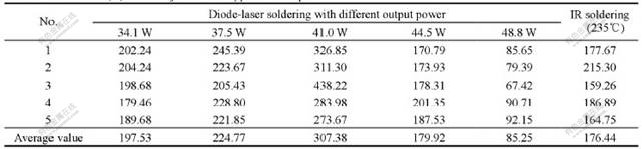
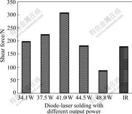
Fig.2 Average shear forces of micro-joints with different techniques
As shown in Fig.2, with the increase of output power of diode-laser, the shear force increases at first, then decreases. When the output power value of diode-laser is about 34.1, 37.5 or 41.0 W, the shear force is much higher than that using IR reflow soldering method, especially when the output power value is about 41.0 W, the shear force exhibits the highest value which is about 70% higher than that using IR reflow soldering method. But the shear force decreases sharply when the output power value is much higher than the optimum value of about 41.0 W. When the output power value is about 48.8 W, the shear force is about 50% of that using IR reflow soldering method.
Fig.3 shows the shear curves of micro-joints with diode-laser soldering and IR reflow soldering. It is clear that from Fig.3, there is an obvious yield point elongation on the shear curve when the output power value is about 37.5 and 41.0 W, as well as using IR reflow soldering. While as shown in Fig.3(c), there is no yield point elongation on its shear curve when the output power value is about 48.8 W, so it can be inferred that the fracture mechanism of soldered joints pertains to the brittle fracture in this instance.
3.2 Analysis of microstructures of micro-joints
Microstructures of micro-joints soldered with Sn- Ag-Cu lead-free solder on Au/Ni/Cu pad are shown in Fig.4, micro-joints of Figs.4(a), (b) and (c) are soldered with diode-laser, and the output powers are 37.5, 41.0 and 48.8 W respectively, micro-joint of Fig.4(d) is soldered with IR reflow.
In Fig.4, tinge ��-Sn grains are surrounded by dark eutectic regions, which consist of Ag3Sn, Cu6Sn5 and ��-Sn ternary eutectic[14]. The difference of shear force of micro-joints is caused by the changes of the microstructures, especially the size change of ��-Sn grains and intermetallic compound particles. The shear strength of the Sn-Ag-Cu alloy system mainly depends on the fine eutectic network structures, and the dispersion morphology of fine Ag3Sn in the eutectic network[15].
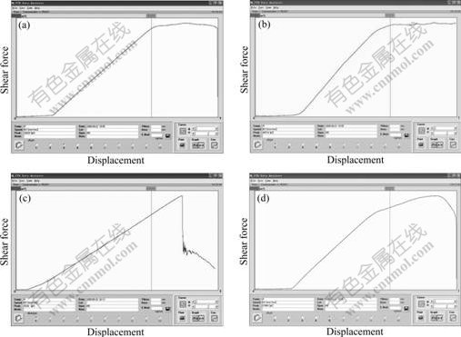
Fig.3 Shear curves of micro-joints with diode-laser soldering and IR reflow soldering: (a) P=37.5 W; (b) P=41.0 W; (c) P=48.8 W; (d) IR reflow soldering
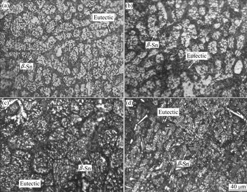
Fig.4 Optical images of Sn-Ag-Cu micro-joints with different techniques: (a) P=37.5 W; (b) P=41.0 W; (c) P=48.8 W; (d) IR reflow soldering
The microstructures in Figs.4(a) and (b) are the typical microstructures of Sn-Ag-Cu solder, with ��-Sn island surrounded by a fine eutectic network. Especially in Fig.4(b), the crystal grains are fine, and the microstructures of the micro-joints are most homogeneous of all; the fine compound Ag3Sn as the strengthening phase, corresponds to the dispersion strengthening theory, making the shear force of the micro-joints exhibit the highest value.
In Fig.4(c), the excess output power results in the phenomenon of superheat, and coarser ��-Sn grains can be found in the microstructures. In the process of solidification, the residual liquid phase is partitioned by the coarse grains, so the solidification shrinkage come from the residual liquid phase can not be replenished in time, which results in the formation of voids, as shown in Fig.5[16].
Furthermore, the excess output power accelerates the mutual diffusion of Sn and Ni atoms from solder and Ni/Au coating respectively, and the formation of intermetallic compound is also accelerated, so the residual coating is thinner than that in other micro-joints. Due to the thermal cycle in the subsequent service conditions, the different diffusion speed of Sn and Ni results in the formation of Kirkendall voids, which leads to the strength reduction of micro-joints and the brittle fracture[7,17].
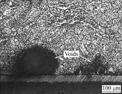
Fig.5 Voids between coating and solder
Attention must be paid to the existence of coarse Ag3Sn plates besides the dispersion morphology of fine compound Ag3Sn in Fig.4(d), which can be seen more clearly in Fig.6.
The cooling speed with IR reflow soldering is lower than that using diode-laser soldering method, so the coarse Ag3Sn plates solidify first, providing nucleation sites for eutectic dendrites[15]. The formation of coarse Ag3Sn plates that are quite brittle must be avoided because they induce defects in soldered joints under low stress or some cyclic stress in service. As a result of the existence of coarse Ag3Sn plates, the shear force of micro-joints soldered using IR reflow soldering method is lower than that using diode-laser soldering system.
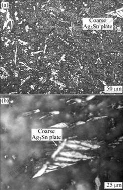
Fig.6 Optical images of coarse Ag3Sn plates
4 Conclusions
1) The formation of intermetallic compound Ag3Sn is the key factor to affect the shear force, and the fine eutectic network structures of micro-joints as well as the dispersion morphology of fine compound Ag3Sn, in which eutectic network band is responsible for the improvement of the shear force of micro-joints soldered with Sn-Ag-Cu lead-free solder.
2) With the increase of the output power value of diode-laser, the microstructures of Sn-Ag-Cu solder micro-joints change obviously. When the output power value of diode-laser is about 41.0 W, the microstructures of the micro-joints are homogeneous, the crystal grains are fine, and the shear force of the micro-joints exhibits the highest value, which is about 70% higher than that using IR reflow soldering method. Because of the existence of coarse Ag3Sn platelets, the shear force of micro-joints soldered with IR reflow soldering method is lower than that using diode-laser soldering method.
References
[1] ABTEW M, SELVADURAY G. Lead-free solders in micro- electronics [J]. Materials Science and Engineering R, 2000, 27(5-6): 95-141.
[2] SUGANUMA K. Advances in lead-free electronics soldering [J]. Current Opinion in Solid State and Materials Science, 2001, 5(1): 55-64.
[3] WU C M L, YU D Q, LAW C M T, WAN L. Properties of lead-free solder alloys with rare earth element additions [J]. Materials Science and Engineering R, 2004, 44(1): 1-44.
[4] XUE Song-bai, YU Sheng-lin. Preparation and characterization on micron power solder of Sn-Ag-Cu-RE [J]. Transactions of the China Welding Institution, 2004, 25(6): 1-3. (in Chinese)
[5] KERR M, CHAWLA N. Creep deformation behavior of Sn-3.5Ag solder/Cu couple at small length scales [J]. Acta Materialia, 2004, 52(15): 4527-4535.
[6] SHOHJI I, YOSHIDA T, TAKAHASHI T, HIOKI S. Tensile properties of Sn-Ag based lead-free solders and strain rate sensitivity [J]. Materials Science and Engineering A, 2004, 366(1): 50-55.
[7] ZENG K, TU K N. Six cases of reliability study of Pb-free solder joints in electronic packaging technology [J]. Materials Science and Engineering R, 2002, 38(2): 55-105.
[8] LI De-zhi, LIU Chang-qing, CONWAY P P. Characteristics of intermetallics and micromechanical properties during thermal ageing of Sn-Ag-Cu flip-chip solder interconnects [J]. Materials Science and Engineering A, 2005, 391(1-2): 95-103.
[9] ZHOU De-jian, WU Zhao-hua. Surface Mount Process Technology [M]. Beijing: National Defence Industry Press, 2002. (in Chinese)
[10] BACHMANN F. Industrial applications of high power diode lasers in materials processing [J]. Applied Surface Science, 2003, 208-209: 125-136.
[11] LI Ming-yu, WANG Chun-qing, BANG H S, KIM Y P. Development of a flux-less soldering method by ultrasonic modulated laser [J]. Journal of Materials Processing Technology, 2005, 168(2): 303-307.
[12] YAO Li-hua, XUE Song-bai, WANG Peng, LIU Lin. Effect of diode-laser parameters on tensile strength of QFP micro-joints [J]. Transactions of the China Welding Institution, 2005, 26(10): 90-92. (in Chinese)
[13] XUE Song-bai,YAO Li-hua, HAN Zong-jie, LIU Lin. Effect of diode-laser parameters on wettability of Sn-Ag-Cu solder [J]. Transactions of the China Welding Institution, 2005, 26(12): 39-42. (in Chinese)
[14] SUGANUMA K. NING Xiao-shan (Tr.). Lead-free Soldering Technology [M]. Beijing: Science Press, 2004. (in Chinese)
[15] KIM K S, HUH S H, SUGANUMA K. Effects of cooling speed on microstructure and tensile properties of Sn-Ag-Cu alloys [J]. Materials Science and Engineering A, 2002, 333(1-2): 106-114.
[16] ZHOU Yao-he, HU Zhuang-lin, JIE Wan-qi. Solidification Technology [M]. Beijing: China Machine Press, 1998. (in Chinese)
[17] SHAWKRET A, DU Li-guang, SUN Zhi-guo, SHENG Mei, LUO Le. Effects of aging and thermal cycling on the microstructure and shear strength of SnAgCu surface mount solder joint [J]. Acta Metallurgica Sinica, 2001, 37(4): 439-444. (in Chinese)
Corresponding author: XUE Song-bai; Tel: +86-25-8489670; E-mail: xuesb@nuaa.edu.cn
