
������ʱ��: 2018-08-24 16:25
����ʱЧ���ζ�Cu-Zr�Ͻ���֯�����ܵ�Ӱ��
�Ͼ�������ѧ���Ͽ�ѧ�빤��ѧԺ
�Ͼ�������ѧ���������Ƽ��о���
ժ Ҫ��
��ȱ���ǽ������ϻ�е���������ܵ���Ҫ����ý�顣������ȱ�ݵ�����ƺ�ZrԪ���Ͻ�,���ö���δ����Ա�����ʱЧ���ս���Ʊ���һ�ָ�ǿ�ȡ��ߵ����Ե�Cu-0.08%(��������)Zr�Ͻ�ʹ�õ��ӱ�ɢ��������(EBSD)�����������(TEM)�����Ͻ����Ʊ�����������֯���ݻ�,����Cu-Zr�Ͻ�Ļ�е���������ܽ��в��ԡ���֯��������:ͨ��������ZrԪ��, Cu-Zr�Ͻ����ǴӵȾ��DZ���(ECAP)�Ĺ���������ת��Ϊһ��ʱЧ���Zrƫ���ȶ��ij�ϸ���Ͻ�,����ͨ�����������Ʊ������׳߶ȵ�Cu-Zr�Ͻ�Ƭ����֯�����ܲ��Ա���, Cu-Zr�Ͻ�EACA(ECAP+aging+cryo-rolling+aging,���ΪEACA)�������ø�Ӳ��(HV 192.6)�ߵ絼��(82.5%IACS)�����ô��䡣������Ϊ,���ǿ����Դ��ϸ��ǿ����ƫ��ǿ�����˻�ǿ���ȶ�ǿ�����Ƶ����,���ߵ������������ڻ����ڲ��͵�Ԫ�ع������͵͵ľ�����䡣����Ϊ�ߵ絼Cu�Ͻ��ǿ���ṩһ���µ����˼·,�����ڹ�ҵ������ʵ�ִ��ģӦ�á�
�ؼ��ʣ�
Cu-Zr�Ͻ�;�Ͻ�;��ȱ��;ƫ��;�˻�ǿ��;
��ͼ����ţ� TG156.92;TG146.11
����飺�����(1993-),��,���ճ�����,˶ʿ,�о�����:�������Ա��Ρ�ͭ�Ͻ�,E-mail:wangjinghao0314@foxmail.com;*������,����;�绰:13770836300;E-mail:jtwang@njust.edu.cn;
�ո����ڣ�2018-07-14
����������Ȼ��ѧ������Ŀ(51520105001);�����ص�����о���չ�ƻ���Ŀ(2012CB932200)����;
Effect of Two-Step Aging and Deformation on Microstructure and Properties of Cu-Zr Alloy
Wang Jinghao Jiang Yao Zhu Yebing Gu Ruicong Liu Ying Wang Jintao
School of Materials Science and Engineering,Nanjing University of Science and Technology
Herbert Gleiter Institute of Nanoscience,Nanjing University of Science and Technology
Abstract��
Defects are the key to control both mechanical and physical properties of metallic materials. Based on intrinsic defect manipulation and micro-alloying with Zr, Cu-0.08%(mass fraction) Zr alloy of high strength and high electrical conductivity was prepared using multiple severe plastic deformation and aging method. Electron backscatter diffraction(EBSD) and transmission electron microscopy(TEM) were used to characterize microstructural evolution during preparation, and mechanical and physical properties were also tested. The results showed that with the addition of Zr, Cu-Zr alloy changed from super-saturated solid solution after equal-channel angular pressing(ECAP) into ultrafine grained alloy with Zr segregation after aging, then the Cu-Zr alloy structure of nano-lamellar was prepared by cryo-rolling. It demonstrated that Cu-Zr alloy possessed high hardness(HV 192.6) and high electrical conductivity(82.5% IACS) after EACA(ECAP+aging+cryo-rolling+aging, EACA). It was found that the high strength originated from the combination of fine-grained strengthening, twin boundary strengthening and ��strengthening by annealing��, while the high electrical conductivity was due to low element solid solution and lattice distortion in the grain interior. The study offered a novel design approach for strengthening Cu-based alloys, which could be efficaciously utilized into manufacturing production.
Keyword��
Cu-Zr alloy; micro-alloying; micro-defects; grain boundary segregation; annealing strengthening;
Received�� 2018-07-14
���Ÿ߿Ƽ���ҵ�ķ�չ, ��߸�ǿ�Ⱥߵ����Ե�Cu�Ͻ��ڵ��ӹ�ҵ���������������е�����
�����������, ���Ի�����ȱ�ݵ������, ���ô����Ա��β�����������, ��ͨ���Ͻ�Ԫ���ȶ�������ʵ�ָ�ǿ��, ���������ȴ������;����ڲ��ľ��������ά�ָߵĵ����ԡ� ������������, �Ͻ�ZrԪ����һ���������ȶ�����ǿ��
1 ʵ ��
����ҵ���ȵ�Cu����Ӧ����������Zr���������Ʊ�Cu-0.08% Zr�Ͻ������� ���, �������г�32 mm��32 mm��160 mm�ķ���, ��850 ���½���1 h�Ĺ��ܴ�����ˮ����ȴ�� ���ܺ�, ����ʹ��8����Bc��ʽ(���90��, �ڽ�20��)��ECAP��Cu-Zr�Ͻ�ϸ������ϸ���߶�, ������1 h 300 ���һ��ʱЧ����(1st aging)�� ����, ������ECAP��ͬ�ı��η������Һ�����Ʊ��Ρ� �������Ϊ����Ʒ����Һ���н���5 min���������, ÿ���μ���10%�ĺ��, һ�����ν��������������Ϸ���Һ���н���, �ټ�����һ����, ֱ��ѹ�����ﵽ90%�� ���, ��300 �����0��5 h�Ķ���ʱЧ(2nd aging)������ �ں�����, �������ռ��ΪEACA (ECAP+aging+CYR+aging)�� Ϊ��̽��ZrԪ���ڴ����Ա��κ�ʱЧ���������ж�Cu�Ͻ�����֯���ܵ�Ӱ��, ���Ļ���ECAP+CYR+aging�ӹ�����Ʒ��Ϊ����������, ���ΪECA, ��ϸ�������1��ʾ��
��֯EBSD����ʹ�ð�װ��AURIGAɨ��羵�ϵĵ��ӱ�ɢ��������(electron backscatter diffraction, EBSD), ���ݷ���ʹ�÷�������Channel 5, ��Ʒ��ͨ���������Ʊ��� ʹ��TECNAI G2 20���������(transmission electron microscopy, TEM)��ʵ����Ʒ���и�Ϊ�۵Ĺ۲�, ������Ʒͨ�����˫�緽���Ʊ���
��������ʵ��ʹ��Shimadzu Universal Testing Machine AGS-100NXʵ���, ʹ�ñ��ߴ�Ϊ 2 mm��7 mm��30 mm�Ĺ����������Գ�ʼӦ������1��10-3 s-1���С� ʵ��ǰ�����������������, ��ÿ�������µ���Ʒ������3�����������ȷ������ظ��ԡ� ��Ӳ��(HV)����ʹ��HVS-5Z����Ӳ�Ȳ�����, ѹ��Ϊ9.8 N, ʱ��Ϊ10 s, ��������ǰ��������������档 Cu-Zr�Ͻ�ĵ絼��ʹ��D60K�����ֵ絼�ʲ����ǽ��в���, λ���ܶ���Bruker D8 X�����������Ͻ��в���, ��Ʒ����ǰ����ͬ��������е�����
��1 ��������ʵ�����
Table 1 Experimental process of two specimens
Samples |
Process steps |
|||
| ECAP | First-step aging | Cryo-rolling | Second-step aging | |
| ECA | Route Bc 8 passes |
/ | Reduction 90% |
300 �� |
EACA |
Route Bc 8 passes |
300 �� 1 h |
Reduction 90% |
300 �� |
2 ���������
2.1 ECAP��ECAP��һ��ʱЧ��������֯����
ͼ1(a), (b)ΪECAP��Cu-Zr�Ͻ��IPF(inverse pole figure)����֯ͼ��;����ߴ�ֲ��� �������, ͨ�����б���
2.2 Һ���������ƺ���֯����
ͼ2ΪECAP��δ��ʱЧ�Ͻ�(ECA��Ʒ)�;�1hһ��ʱЧ�Ͻ�(EACA��Ʒ)Һ���������ƺ������ϵ�TEM�����������Ƭ����ͳ�ƽ���� ���ֲ�ͬ״̬��Cu-Zr�Ͻ����ƺ�, ����֯���������Ըı䡣 ECAP��ֱ�ӵ������Ƶ�Cu-Zr�Ͻ�(ECA��Ʒ)��ԭ���϶����ά״���Ǿ�����֯��ʧ, ת��Ϊ�������Ʒ���(rolling direction, RD)�IJ�Ƭ״��֯�� ��һ��ʱЧ�����Ƶ�Cu-Zr�Ͻ�(EACA��Ʒ)���ɳ�ϸ���ĵ��ᾧ��ת��ɲ�Ƭ״�ṹ��
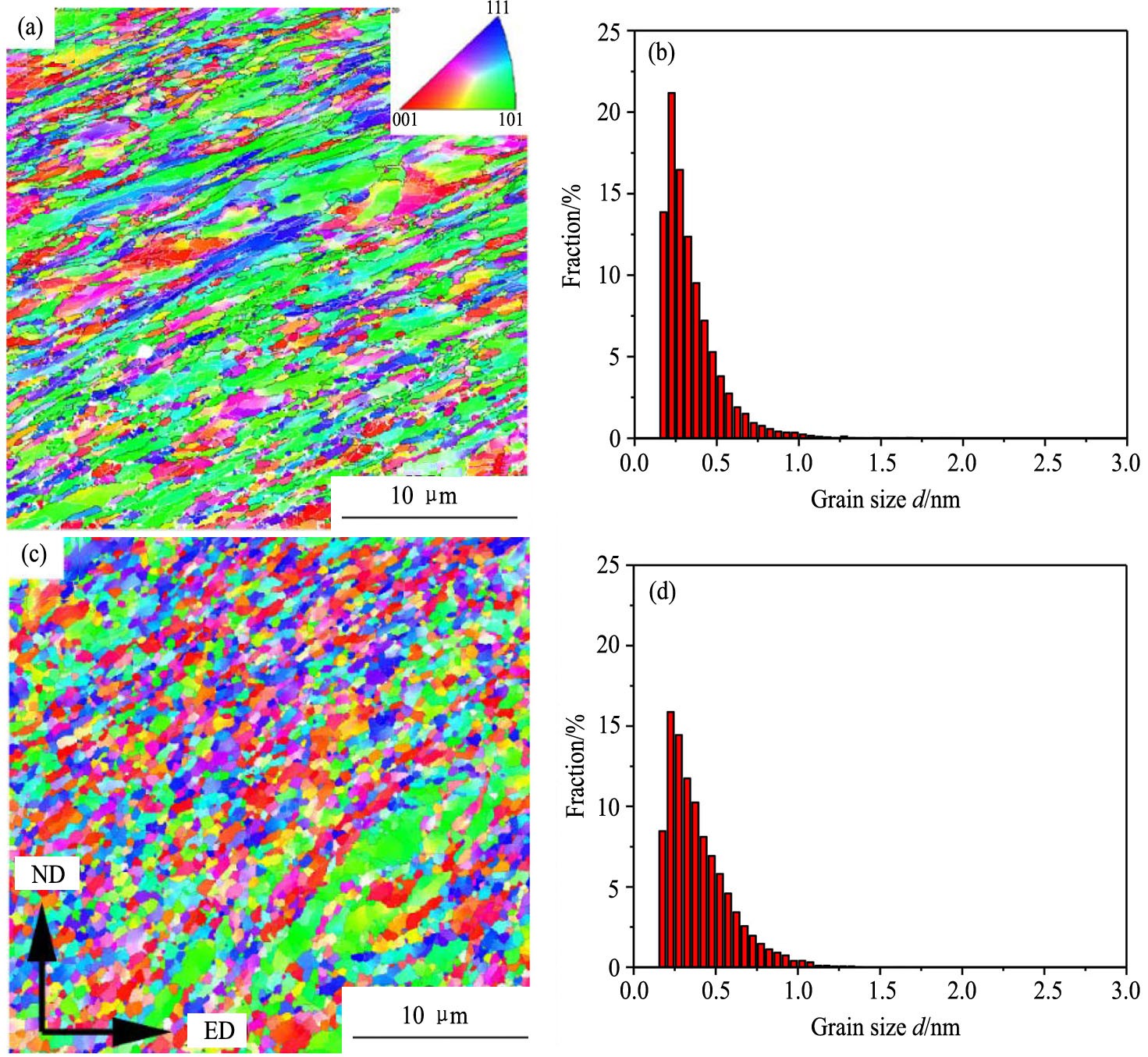
ͼ1 Cu-Zr�Ͻ�ECAP���300 �� 1 hһ��ʱЧ�������EBSD����֯ͼ��(ͼ�к���Ϊ�Ƕȴ���15��Ĵ�ǶȾ���, ����Ϊ2�㡫15��С�ǶȾ���)�;����ߴ�ֲ�
Fig.1 Microstructure of Cu-Zr alloy after ECAP and first aging characterized by EBSD and grain size distribution
(a)IPF image on transverse direction(TD)after ECAP;(b)Grain size distribution of the alloy after ECAP;(c)IPF images on TDafter aging for 1 h under 300��;(d)Grain size distribution of the alloy after aging for 1 h under 300��
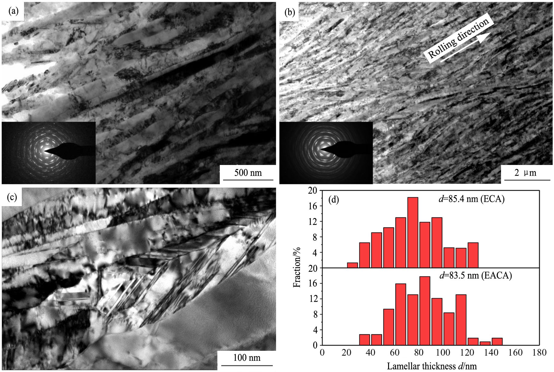
ͼ2 Һ�����Ƶ�Cu-Zr�Ͻ�TEM�������Ƭ���ȷֲ�
Fig.2 Microstructure characterization of Cu-Zr alloys after cryo-rolling and lamellae thickness distribution
(a)TEM image of ECA specimen after cryo-rolling;(b),(c)TEM images of EACA specimen after cryo-rolling;(d)Nano-layer thickness distribution of ECA specimen and EACA specimen
���ݼ���ϸ��ЧӦ, ������֯�����ƹ����еı��������ŷ���(normal direction, ND)��ѹ�����κ�RD������������Ϊ���� ����ȫ���ؼ���ϸ���ı���������, 90%��ѹ������Ӧʹ�����ߴ��ں�ȷ����Ϊԭ���ߴ��10%�� ����ʵ�ʶ���, ����Ӧ����������, �����ߴ粢δ�ﵽ����ϸ���ijߴ�, ���Ǵﵽһ����������ֵ����̬�����ߴ硣 ��̬�����ߴ�Ĵ�����ζ���ڱ��ι����д����Żָ�����, �ָ��������ű��ι��̳�������Ӧ�������ϸ���� ��̬�����ߴ��ƽ��̬��λ�����ߴ��й�, ���ӹ�Ӳ��(λ����ֵ)�Ͷ�̬�ظ�(λ������ ����)֮��ﵽƽ��
2.3 ����ʱЧ��Cu-Zr�絼�ʵ�Ӱ��
ͼ3ΪEACA��Ʒ��ECA��Ʒ�ڶ���ʱЧ�����еĵ絼����ʱЧʱ��仯���ߡ� ����̬��Cu-Zr�Ͻ�絼��Ϊ82% IACS, ����ECAP֮��, ������֯��λ���� ȱ�ݵļ�����Cu����������ػ���, ����Cu-Zr�Ͻ�絼���½���75% IACS, �½�Լ7% IACS�� Һ������������, �ڳ��ڵ�1 h����ʱЧ�����е絼�ʶ��Ǵ��ڿ������߽�, ����ʱЧʱ����ӳ�, �絼�ʵ�������������ֱ���絼�ʱ����ȶ�����(EACA��Ʒ�絼���ȶ���85% IACA, ECA��Ʒ�絼�����ȶ���82% IACS����)�� �Ƚ϶���, EACA��Ʒ�ĺϽ�絼���������ʸ���, ��ʱЧ������ʱ��Խ��, ��ECA��Ʒ�ĵ絼�ʲ��Ҳ��Խ�� ����Mattiessen����,�������ܵ�����(��total)���Ա�ʾΪ
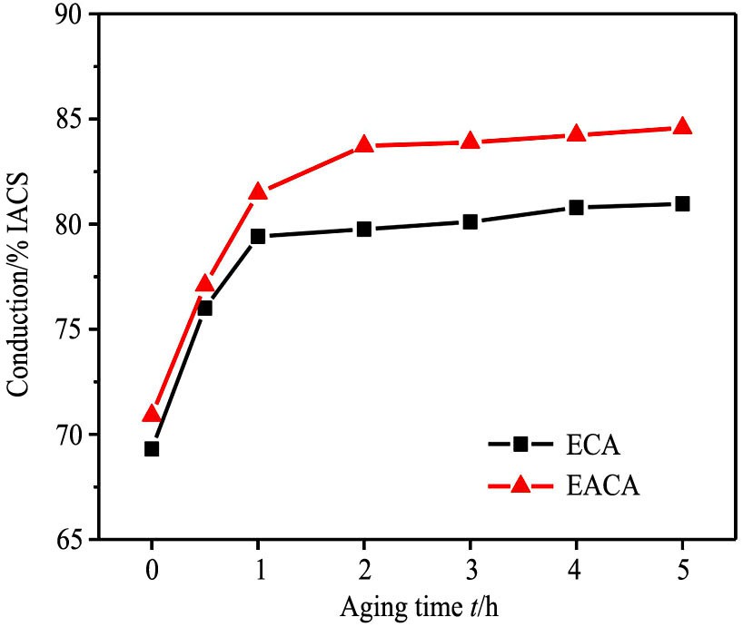
ͼ3 ECA��Ʒ��EACA��Ʒ�ĵ絼����300 �����ʱЧ����ʱ��ı仯����
Fig.3 Electrical conductivity evolution of ECA specimen and EACA specimen with aging time at 300 ��
��total=��t+��i+��d (1)
ʽ����t, ��i����d�ֱ������� ���ʺ;���ȱ�ݶԵ����ʵ�Ӱ�졣 ��Mishnev�Ĺ۵�
2.4 �Ͻ�Zr��Cu-Zr��е���ܵ�Ӱ��
���ڽ����Ͻ�ZrԪ���ڴ����Ա��κ�ʱЧ�����е��ݻ������յ�ǿ�����ƽ�������(ͼ4)�� ����EACA��Ʒ, ������Cu�е�Zrԭ����ECAP���һ��ʱЧ�����л�ͨ��λ����ȱ����̳���ɢ�� TEM����������仨��(ͼ2)��δ�����Թ۲쵽Cu10Zr7��Cu5Zr��������, �����Ϊ��ECAP���ʱЧ�����в���Zrԭ�ӻ����ȴӻ���ƫ��������(GB)��, ����Zr��ͭ���е�ƫ����������������ͬ����Cu-Zr(0%, 0.4%, 1.0%, 3.0%��7.0%)�Ͻ�
��һ����Һ����������ʹ��Cu-Zr�Ͻ��в������������ײ�Ƭ, ͬʱ�������λ���� �����ж���ʱЧ����, ������Cu-Zr�Ͻ��е�ʣ��Zrԭ�ӻ���������ײ�Ƭ�Ľ��洦ƫ���� ��Cu�Ͻ�ķ��Ӷ���ѧģ��������
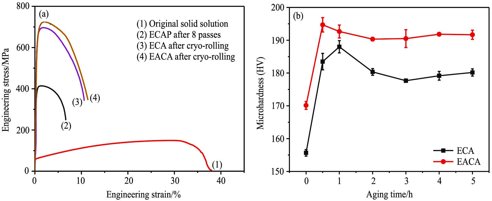
ͼ5(a)Ϊ����ECAP��ѹ�����Һ�����Ʒ�����Cu-Zr�Ͻ�����칤��Ӧ��-Ӧ�����ߡ� ���Կ���, Cu-Zr�Ͻ�Ŀ���ǿ�Ⱥ�����ǿ�����ž����ߴ�Ľ��Ͷ����ߡ� ��ʼ����̬��֯���ԽϺ�, ��ֻ��Լ160 MPa������ǿ�ȡ� �����ECAP��Cu-Zr�Ͻ�410 MPa�Ŀ���ǿ��, �������ƺ��Cu-Zr�Ͻ�������Լ300��330 MPa�ﵽ��700��730 MPa�� ������ͬѹ������, EACA��Ʒ������ǿ�ȺͿ���ǿ�ȶ������ECA��Ʒ������Լ45 MPa, ����ͼ4�е�ǿ�����̷���, ��Ϊ�˴�����������ǿ�ȵ�������Ҫ��Դ��һ��ʱЧ������Zrƫ���� ͬʱ, Cu-Zr�Ͻ������������ECAP���ɹ���̬��38%Ѹ�ٽ�����6%��7%, �������ƺ�������������10%��12%�� ���ڵ������ƺ����Ե�����, ���Թ鹦�ںϽ��ڽ������Ա���ʱ, �����е����������Ͼ�������, ʹ�ô�ͳ�ྦྷ����λ��-���硢 ����λ��֮��Ľ�������ת���Ϊλ�����Ͼ��Ľ������á� ͬʱ, λ�����Ͼ��紦�Ļ��ơ� ������ ��ֳʹ���Ͼ���ʧȥ������, �Ӷ�Э��������������
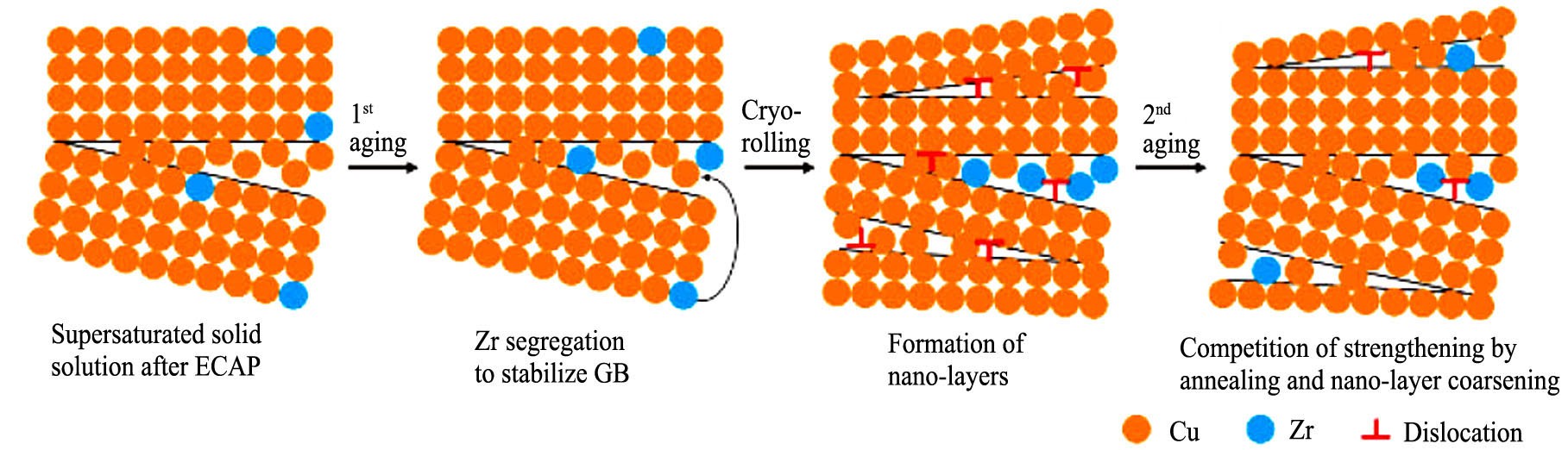
ͼ4 �Ͻ�ZrԪ��ǿ��ʾ��ͼ
Fig.4 Schematic diagram showing the strengthening mechanisms of micro-alloying with Zr
ͼ5 Cu-Zr�Ͻ�Ĺ���Ӧ��-Ӧ�����ߺ�ECA��Ʒ��EACA��Ʒ��300 �����ʱЧ��Ӳ����ʱ��ı仯����
Fig.5 Engineering stress-strain curves of Cu-Zr alloys (a) and vickers hardness evolution of ECA specimen and EACA specimen with secondary ageing time at 300 �� (b)
ͼ5(b)����Cu-Zr�Ͻ����ƺ����ʱЧ������������Ӳ�ȵı仯�� ����һ��ʱЧ��Cu-Zr�Ͻ�(EACA����)���и��ߵ�ǿ��, �����Ŷ���ʱ�������(0��0.5 h), Ӳ�ȳ�����ߡ� EACA������30 min��ʹﵽӲ�ȵķ�ֵ(HV 195), ��ECA��������60 min�Ŵﵽ��ֵ(HV 189)�� ������ʱЧ��, ������Ʒ��֯��ʼ����Ӳ���½������������ȶ��� �������, ���Ŷ���ʱЧ�ļ���, Cu-Zr�Ͻ��ٽᾧ�������κ˺ͻظ��Ĺ����Ѿ��������, ������֯�г������ٽᾧ������
����Tabor��ϵ(H=3��y)��Taylorλ��ģ��
ʽ����0ΪCu�����Ħ��Ӧ��, MΪ̩������, ��Ϊ̩�ճ���, ��Ϊ����ģ��, bΪ����˹ʸ��, ��kH-P��d��ΪHall-Petch (H-P)��ϵ�е�ϵ���;����ߴ硣 ��������Ƭ�㾧�����ǵ��ᾧ��, TEMͼ���е�����ƽ�������ߴ�С�ں���, ���Խ�Լ85��110 nm�ľ����ߴ����X��������(XRD)���Եó���λ���ܶ�Լ1.5��1015 m-2����ʽ(2)�м���ó���Cu-Zr�Ͻ������Ӳ��ֵΪHV 150��160, �˽����ECAʵ��ó���Ӳ��(HV 156)ֵ��Ϊ�ӽ��� ����ECA��EACA�����������ƺ�HV 15��ǿ�Ȳ�ֵ, ������Tabor��ϵ����ó�Լ49 MPa������ǿ�Ȳ�ֵҲ�����������е�45 MPa�Ľ�������Ǻϡ� �ɴ˿���Ϊ, �ں����Ķ���ʱЧ��, ��ZrԪ�ص�ƫ�����˻�ǿ����ͬ����Cu-Zr�Ͻ�ǿ��, �������������ٽᾧ���������γɶ�̬ƽ�⡣
ͨ�����������������ƺ��TEM��֯ͼ���ʱЧ�����е絼�ʡ� ��Ӳ�ȵı仯����, ���Կ��������ECAP��ֱ�ӵ�������, �ڱ�֤��ϸ����֯������ȫ����������½����ʵ���һ��ʱЧ��������������ں�����ʱЧǿ���дٽ��Ͻ�絼�ʺ�Ӳ�ȵ������� ����EACA��Ʒ, Cu-Zr�Ͻ�ӵ�и��õ�����Ƭ��ϸ��Ч��, ����ʱЧǿ����Ҳ���ڸ��̵�ʱ���ڴﵽ��ǿ�ߵ����ۺ�����, ���پ������ٽᾧ��������ܵIJ���Ӱ�졣
3 �� ��
ͨ���Դ�ͭ��Zr�Ͻ�, ���ECAP�� Һ���������ƺ�ʱЧ�����ɹ��Ʊ������ײ�״Cu-Zr�Ͻ�, ��ʵ�ֶ���ʱЧ�и�Ӳ��(HV 192.6)�ߵ絼��(81.5% IACS)�����ô��䡣 ����Ҫ������:
1. ����ZrԪ��(0.08%)����������ECAP��ϸ��Cu-Zr��֯��һ��ʱЧ�����е����ȶ���, �־�����֯��ʱЧ�����еĿ����ٽᾧ������Ϊ��
2. һ��ʱЧ�����ܴ�ʹ���ڵ�ZrԪ����Ǩ��, �������彵�;����ܺ��ȶ����硣 �����ܴﵽ�����Ͻ�絼�ʡ� ���ǿ�Ⱥͽ�������Ƭ�����Ч����
3. �ڶ���ʱЧ������, Cu-Zr�Ͻ�����ܱ仯�����˻�ǿ���� ƫ��ǿ�����ٽᾧ����3�ֻ�����ۺϵĽ���� �����Գ������߲������ȶ���85% IACS, Ӳ��������0.5��1.0 h����������ֵ, ����ʼ�½����γɶ�̬ƽ�⡣
�����
[8] Saarivirta M J.High conductivity copper-rich Cu-Zr alloys [J].Trans.Met.Soc.Aime.,1960,218.
