

Annealing effect and irradiation properties of HFCVD diamond films
REN Ling(�� ��)1, WANG Lin-jun(���־�)1, SU Qing-feng(�����)1, LIU Jian-min(������)1, XU Run(�� ��)1, PENG Hong-yan(������)2, SHI Wei-min(ʷΰ��)1, XIA Yi-ben(���屾)1
1.School of Materials Science & Engineering, Shanghai University, Shanghai 200072, China;
2.Physics Department, Mudanjiang Normal College, Mudanjiang 157012, China
Received 10 April 2006; accepted 25 April 2006
Abstract:
The post-growth treatment of a [100]-oriented diamond film was performed to improve the film quality. The characteristic of post-growth film was investigated by using the RAMAN spectrum and the capacitance-frequency curve. The results show that the resistivities and frequency response enhance after the post-treatments in solution of H2SO4 and H2O2 and an annealing under N2 atmosphere at 500 �� for 60 min. Under a bias voltage of 100 V, the net photocurrent is obtained under 55Fe(5.9 keV) X-rays and 241Am (5.5 MeV) a particles radiation, respectively. The photocurrent increases rapidly at first and becomes stable for the ��pumping�� effect with the radiation time.
Key words:
diamond film; hot filament chemical vapor deposition(HFCVD); annealing; radiation;
1 Introduction
Diamond used as semiconductor material exhibits many outstanding features such as chemical inertness, irradiation hardness and wide band gap. Other desirable properties of diamond for use as a nuclear radiation detector include high electron and hole mobilities (1 800 and 1 200 cm2/(V?s), respectively), and a high electrical breakdown of 107 V/cm[1]. For potential application of diamond in superconducting supercollider, it is essential that the system detectors withstand the extreme radiation fields from high-energy and high-intensity beams anticipated during its operation[2].
Especially, with the development of chemical vapor deposition (CVD) technique, CVD diamond film has been interested in wide fields[3]. Several studies have shown that chemical vapor deposited diamond could enable the fabrication of materials exhibit optical and electrical properties similar or superior to those of some of the best natural gems[4, 5].
An important issue still to be mastered, however, is the effect produced by polycrystalline film microstructure, established during the growth phase, insofar as the defected regions among the grains (grain-boundaries) appear to be the main reason for the response limitations compared to the single crystal diamond. This aspect is even more critical if the final application requires high quality thin-films[6].
Otherwise, wide applications of diamond-devices fabrication comprise a number of processes besides the growth of a high quality crystalline diamond film. These processes include etching, doping, annealing, etc. The properties of the diamond film after these processes play an important role in the fabrication of the diamond-devices.
This work mainly focused on the post-treatment of the diamond film for radiation detectors. After the post treatment, its performance was improved. Then irradiation response measurement was carried out to settle the base of fabricating high efficient radiation detector.
2 Experimental
The diamond film was grown on [100]-oriented silicon substrate by hot filament chemical vapor deposition (HFCVD). The growth process and parameters were given in detail in Ref.[7].
One as-grown sample was annealed under N2 atmosphere at 500 �� for 60 min in order to remove the hydrogen-rich surface, and then cleaned with a solution of H2SO4 and H2O2 for 30 min in order to remove any surface conductive layer.
Following these chemical treatments, a thermal evaporation method was used to deposit Cr/Au(50 nm /150 nm) composite electrode(1 mm in diameter) onto the diamond film as the signal output. After that, it was annealed under N2 atmosphere at 450 �� for 45 min again. The same electrodes were directly deposited on the other one without any post treatment.
55Fe and 241Am were used as X-ray and a particle sources placing above the detector sitting a distance of
1 cm in air at room temperature. Keithley 4 200-SCS was used to measure the current-voltage characteristics of these detectors with and without 5.9 keV X-ray and 5.5 MeV a particle irradiation.
3 Results and discussion
For the same growth parameters, the grain size of HFCVD diamond film is about 6 mm(Fig.1), which is obviously [100]-oriented. It is always reported that [100]-oriented diamond film has the best electrical properties and surface smoothness to fabricate high quality radiation detector, for it is well known that the detector response is strongly influenced by the phase purity and the crystalline perfection of the active material. Impurity centers, acting as trap states, lower or, depending on their density, even inhibit the collection of carriers generated by the passage of ionizing particles through the device[8].
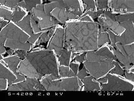
Fig.1 SEM image of diamond film deposited by HFCVD on silicon substrate
The dark current versus applied voltage (I-V) curve(Fig.2) shows the diamond films before and after annealing. The dark current decreases a few orders that of magnitude after post treatment, which indicates its resistivity is extremely raised. The curve exhibiting strict linearity after annealing implicates the perfect ohmic contact between CVD diamond film and the composite electrode.
The reason for the observed change in resistivity is related to saturating of the C suspension bonds in diamond film by some H atoms while others are under the state of electrical activity during deposition, which results in the low resistivity. Either the movement of electrical-active hydrogen out of the film or converting to nonelectrical-active hydrogen is due to the rise of the resistivity after post treatment[9-11].
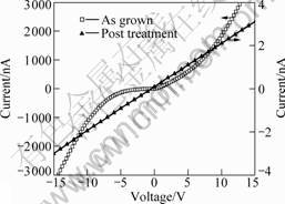
Fig.2 I-V curve of diamond film before and after post treatment
Fig.3 shows the comparison of frequency response between two diamond films. The dielectric loss has a gradual drop at low frequency while becomes stable at high frequency. Its capacitance is more close to the dielectric constant of natural diamond (5.7) after post treatment. It is known that the dielectric constant is affected by two independent factors: graphic content and crystal quality, and diamond content and quality. For conductivity of graphite is several orders of magnitude higher than diamond and non-crystal carbon, it greatly restricts the enhancement of dielectric property. The dielectric property greatly depends on H content and non-diamond phase which is reduced by the post treatment in the thin film as shown in Fig.3, contributing to the improvement of film property.
Fig.4 shows a typical RAMAN spectrum of the post-growth diamond film for further study. It has a sharp characteristic peak at 1 335.1 cm-1 with a small full width at half maximum and a weak graphite peak at 1 550 cm-1. The region of 1 400-1 600 cm-1 has a very broad weak band and fluorescence background caused by non-diamond phase. For the sensitivity ratio of nondiamond to diamond phase is about 75 times in RAMAN signal, revealing that the diamond had a good quality.
Fig.5 shows the capacitance under various frequencies for diamond film after post treatment. From
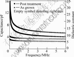
Fig.3 Capacitance and dielectric constant with frequency change for diamond films with and without a post treatment
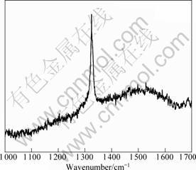
Fig.4 RAMAN spectrum of post-treatment diamond film
Fig.5, it can be seen that capacitance has troughs and peaks with the change of the voltages when the signal frequencies are low. It is the charges in the diamond film or the offset of the work function that has impact on the characteristic of C-V. With the increase of the frequency, capacitance gradually reduces and keeps constant with the rise of the frequency, demonstrating that the diamond film has good response to high frequency.
The principle of radiation detection in diamond is based on the creation of electron-hole pairs within the diamond from the interaction of the incident particles to be detected. The local displacement of these electrons and holes driven by an electric field in the diamond will induce a transient signal on the detector electrodes[12]. Fig.6 shows the photocurrent response of the diamond detector. Curves (a) and (b) are the net photocurrent which is the difference between whole current and dark current under X-ray and a particles radiation, respectively(The photocurrents mentioned in the following text are all net photocurrent). At 100 V bias voltage, the photocurrents are 15.9 nA and 7.0 nA under X-ray and a particles irradiation, respectively.
The curve of photocurrent versus irradiation time(Fig.7) is given to investigate trapping effect of carriers under 5.9 keV X-ray irradiation. The value of photocurrent goes up rapidly at first and keeps saturation state with the irradiation time. However, for the diamond
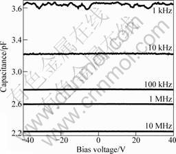
Fig.5 Capacitance under varied frequency for diamond film after post treatment
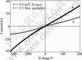
Fig.6 I-V characteristic of diamond film detector under X-ray irradiation (a) and a particle irradiation (b)
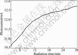
Fig.7 Photocurrent change tendency with time elapsing under X-ray irradiation(5.9 keV 55Fe X-ray irradiation on CVD diamond detector with a distance of 1 cm frontside electrode supplied with bias voltage of 100 V and backside electrode grounded)
film is polycrystalline structure, the impurities and defects that act as trapping and recombination sites for the carries mainly locate at the grain boundaries. Thus, the presence of defects and impurities within the active material may severely reduce the carrier free path, limiting the charge collection distance due to the server scattering between the grain boundaries when the carries are under external bias voltage. At the beginning of the irradiation, a great deal of trapping centers are filled with electrons and holes ionized by X-ray contributing to the increment of collecting charges, continual photocurrent increasing with the irradiation time. After some time, photocurrent gets saturation when the number of efficiency trapping centre and trapped carriers are in dynamic equilibrium, which is called ��pumping�� effect. The property of detector gets stable and the sensitivity enhances. Therefore, the detector can be pre-irradiated for some time to get steady before operating. So is the detector when irradiated with a particles.
4 Conclusions
1) We could control the growth parameters to obtain a [100]-oriented CVD diamond film containing less grain boundaries for fabrication of radiation detector.
2) Surface process and annealing step can efficiently reduce the defects and impurities on or under the shallow surface. For this reason, post-growth treatments are the important steps to improve CVD diamond film��s properties such as ohmic contact and resistivity.
3) At 100 V bias voltage, the net photocurrent is obtained as 15.9 nA and 7.0 nA under the irradiation of X-ray 55Fe(5.9 keV) and a particles 241Am (5.5 MeV), respectively. The photocurrent increases rapidly at first and becomes stable for the ��pumping�� effect with the irradiation time.
4) The detector could be irradiated before operation to become stable, which would improve the property of the detector.
References[1] GALBIATIA A, BREESEA M B, KNIGHTSB A P, SEALYB B, SELLIN P J. Characterisation of a coplanar CVD diamond radiation detector[J]. Nuclear Instruments and Methods in Physics Research A, 2001, 466: 52-57.
[2] DILAWAR N, KAPIL R, VANKAR V D, AVASTHI K D, KABIRAJ D, MEHTA G K. Radiation hardness of polycrystalline diamond thin films irradiated with 100 MeV I7+ ions[J]. Thin Solid Films, 1997, 305: 88-94
[3] JANY C, FOULON F, BERGONZO P, MARSHALL R D. Post-growth treatment and contact formation on CVD diamond films for electronic application[J]. Diamond and Related Materials, 1998, 7: 951-956.
[4] DONATO M G, FAGGIO G, MARINELLI M, MESSINA G, MILANI E, PAOLETTI A, SANTANGELO S, TUCCDIARONE A, VERONA R G. High quality CVD diamond for detection applications: structural characterization[J]. Diamond and Related Materials, 2001, 10: 1788-1793.
[5] MAINWOOD A. CVD diamond particle detector[J]. Diamond and Related Materials, 1998, 7: 504-509.
[6] TRUCCHIA D M, CAPPELLIA T E, CONTEB G, MATTEIA G, GRAMACCIONIC C, ASCARELLIA P. The influence of grain-boundaries on the electronic performance of CVD diamond films[J]. Diamond & Related Materials, 2005, 14: 575-579.
[7] ZHANG M L, XIA Y B, WANG L J. Response of chemical vapor deposition diamond detectors to X-ray[J]. Solid State Communications, 2004, 130(6): 425-428.
[8] XIA Y B, SEKIGUCHI T, ZHANG WANG W J. Surfaces of undoped and boron doped polycrystalline diamond films influenced by negative DC bias voltage[J]. Diamond and Related Materials, 2000, 9(9): 1636-1639.
[9] MANCA J V, NESLADEK M, NEELEN M, QUAEYHAEGENS C, SCHEPPER L D, CEUNINCK W D. High electrical resistivity of CVD-diamond[J]. Microelectronics Reliability, 1999, 39: 269-273.
[10] JANY C, TARDIEU A, GICQUEL A, BERGONZO P, FOULON F. Influence of the growth parameters on the electrical properties of thin polycrystalline CVD diamond films[J]. Diamond and Related Materials, 2000, 9: 1086-1090.
[11] LI J Q, SUN Y I, GUO W T, LIANG X A. Several methods for improving the resistivity of diamond films[J]. Vacuum & Cryogenics, 1997, 3(3): 174-177.
[12] BERGONZO P, BRAMBILLA TROMSON D, MER C, GUIZARD B, FOULON F. CVD diamond for radiation detection devices[J]. Diamond Relat Mater, 2001, 10: 631-638.
Foundation item: Project(60577040) supported by the National Natural Science Foundation of China; Project (0404) supported by Shanghai Foundation of Applied Materials Research and Development; Projects(0452nm051, 05nm05046) supported by the Nano-technology Project of Shanghai; Project(T0101) supported by Shanghai Leading Academic Disciplines
Corresponding author: WANG Lin-jun; Tel: +86-21-56333514; Fax: +86-21-56332694; E-mail: ljwang@staff.shu.edu.cn
