
��������̫���ܵ�ؼ�����Ĥ�ṹ��ѧ����
�Ա��ǣ��ܼ̳У������ޣ�������
(���ϴ�ѧ ��Դ��ѧ�빤��ѧԺ, ���� ��ɳ��410083)
ժҪ���ý��书��Ϊ100~500 W��ֱ����Ӧ�ſؽ��䷨�Ʊ�����ͬ�ṹ�����Ե�TiO2��Ĥ��Ʒ������ԭ��������(AFM)��X��������(XRD)������Ҷ�������(FTIR)������ɼ���ֹ��ȼƶԱ�Ĥ����ò���ṹ����ѧ���Խ��б������о����书�ʶԱ�Ĥ�Ľṹ����ò����ѧ���Ե�Ӱ�졣�о��������������̬��Ĥ��Ϊ����ṹ�������ヲ��ģʽ�³����ı�ĤΪ��״̬������ģʽ�³����ı�Ĥ������TiO2��Ĥ�����������Ž��书�ʱ仯��1.8~2.3֮��仯���ڵ����Ʊ��ij���̬��Ĥ����TiO0.5������ʹ��Ĥ��Ʒ�����ʽ��ͣ�����Ҫ��TiO0.5���ԹⲨ��ǿ���������£�400 W���书�����Ʊ����ʺ�̫���ܵ�ؼ�����ĤӦ�õ����ʸ������ʴ��TiO2����Ĥ��
�ؼ��ʣ�
����������ֱ����Ӧ�ſؽ��������书���������䱡Ĥ����ѧ������
��ͼ����ţ�O484 ���ױ�־�룺A ���±�ţ�1672-7207(2011)07-2147-05
Structure and optical properties of
titanium dioxide antireflection thin films for solar cell
ZHAO Bao-xing, ZHOU Ji-cheng, RONG Lin-yan, PENG Yin-qiao
(School of Energy Science and Engineering, Central South University, Changsha 410083, China)
Abstract: TiO2 films with different structure properties were prepared with varying sputtering power from 100 W to 500 W. Film surface morphology, structure, and optical properties were measured with step profiler, AFM, X-ray diffraction, FTIR, UV-VIS transmittance spectroscope and ellipsometry respectively. The influence of the sputtering power on the films structure, morphology and optical properties was investigated. The results show that the deposited films are in disorder state. Films deposited in oxide mode are transparent while those in metal mode are opaque. The refraction index varies from 1.8 to 2.3. The film prepared at low sputtering power possesses TiO0.5 small crystal whose absorption has hindered the transmittance. The optimum sputtering power is 400 W.
Key words: titanium dioxide; DC reactive magnetron sputtering; sputtering power; antireflection; optical property
���ڹ������ϵ��(n~3.5)[1]�����������ϵ�����ܴⲨ�ڽ��洦�ķ����ΪӰ��̫���ܵ��Ч�ʵ���Ҫ���أ���ˣ������ڵ�ر���ӶƼ�����Ĥ������Ĥ�ɷ�Ϊ����/����ķ�֮һ��������Ĥ
1 ʵ��
����ֱ����Ӧ�ſؽ��䷨���Ըߴ������������Ϊ��Ӧ����ͽ������壬�ڲ����ĵ����Ʊ�����TiO2��Ĥ���������ֱ��Ϊ10 cm�ĸߴ�Ti�У��л���Ϊ6 cm������ұ�����ն�Ϊ1 mPa��������ѹΪ0. 7 Pa��O2 ��Ar�����ֱ�Ϊ10��90 mL/min�����书��Ϊ100~500 W������ʱ��Ϊ3~200 min���Ʊ���Ⱦ�Ϊ200 nm��TiO2��Ĥ���Բ��ֱ�Ĥ��Ʒ��N2����������350 �汣��5 min�����˻�������1��ʾΪ�������ղ�����
����Alpha-Step ��̨���Dz�����Ĥ��ȣ������ݳ���ʱ��õ��˳������ʣ���NT-MDT Solver-P47��ԭ���������۲챡Ĥ�ı�����ò������ԭ���������Դ����������ñ�Ĥ���������ķ�ֵRmax�Լ��������ֲڶ�Rrms������D/MAX 2550��X�������Ǻ�Avatar 360��FTIR������������Ĥ���ṹ����TU-1800����-�ɼ���ֹ��ȼƲ�����Ĥ���ʣ����Է�ΧΪ300~900 nm����SGC-2�Զ���Բƫ�����Dz�����Ʒ600 nm�������������ʡ�
��1 �Ʊ�TiO2��Ĥ�Ĺ��ղ���
Table 1 Preparing parameters of TiO2 thin films
2 ���������
2.1 ��������
ͼ1��ʾΪ��ͬ���书���Ʊ���TiO2��ĤAFM���ݽ�����ѹ�ͳĵ��¶ȣ���Thorntonģ��[12] �����жϳ�����Ϊ100��200��400 Wʱ������TiO2��ĤΪ���ܵ���״�ṹ��300 Wʱ�����ı�Ĥ����������ͻ��Ϊ���ɵ���״�ṹ����ͼ1���Կ�����300 Wʱ�Ʊ��ı�Ĥ�ֲڶ����Ϊ21.77 nm��100 Wʱ�Ʊ��ı�Ĥ�ֲڶ���С��Ϊ6.27 nm����ϱ�1���Կ�����300 Wʱ����ʱ�������ʽϿ죬������Ǩ�Ƶ���������ʹ�֮ǰ�ѱ��������������ǣ���ʱ��Ĥ����ֲڶȽϴ�400 Wʱ����ʱ���������������ӣ�����ʱ�����ѹ�ϸߣ��������Ӿ��нϴ�Ķ��ܣ���ԭ�ӵ���ĵ�ʱ�ж������������ԭ���ڱ�Ĥ����Ǩ��һ�ξ��룬��Ĥ����ֲڶȽ�С�������书�ʽϵ�ʱ���б��洦������̬�������ˡ����ж����������书������500 Wʱ�������ﲻ���ڰб���ۼ����б��洦�ڽ���̬������������ӣ������ѹ���ͣ���������ͻ�������������Ӷ��ܵͣ��Ʊ��ı�Ĥ�ı���ֲڶȴ�29.52 nm������������ģʽ�Ĵֲڶȡ�ƽ���ı�����ò���Լ�С�Ⲩ�ڱ�Ĥ�����ɢ����ʧ[13]�������ڹⲨ�������ԣ��Ʊ�������TiO2��Ĥʱ�����书�ʲ��˹��ߡ�

ͼ1 ��ͬ�����Ʊ�TiO2��Ĥ��AFM��
Fig.1 AFM images of TiO2 thin films prepared at different sputtering powers
2.2 ��Ĥ�ṹ����
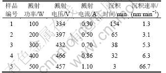
�Բ��ֱ�Ĥ��Ʒ��N2����������350 �汣�� 5 min�����˻�����ͼ2��ʾΪ�˻�ǰ��Ĥ��XRD�ס���ͼ2(a)���Կ�������200~500 W�������Ʊ��ı�Ĥ�������Ե�XRD����壬����Ϊ�ù��ʷ�Χ���Ʊ���TiO2��ĤΪ���νṹ�����书��Ϊ100 Wʱ�Ʊ��ı�Ĥ��2��Ϊ36�㸽������TiO0.5(110)������塣��Ϊ������Է�������С��벵���Է����������ѵ���Է�����������ԭ����Ti�б��汻������ײ����һ�����������ٷ��䵽�ĵ��ϣ���Щ���������ڱ�Ĥ�ᾧ���ʽ����������ʵ��������������ڱ�Ĥ�ᾧ��Ҳ�����Ƶ��о����������ֱ����Ӧ�ſؽ��䣬���������ϴ������������������£���Ĥ�����ڳ������ѿ���TiO2��TiOx (x��2)����[14]��500 Wʱ����̬��Ĥ��55�㸽����1����ΪTi3O5�ࡣ
ͼ2(b)��ʾΪ��N2����������350 �汣��5 min�����˻�������Ʒ��XRD�ס��ɼ���500 W�������Ʊ�����Ʒ�������������Ti3O5���ࣻ100 W�������Ʊ�����Ʒ��TiO0.5 (110)���������ʧ�����ֽ��ʯ��TiO2 (101)������塣��ˣ�100 W���书�����Ʊ��ı�Ĥ�Ǻ���TiO0.5���Ĺ���������TiO2��Ĥ��
ͼ3��ʾΪ��ͬ���书���³�����Ĥ��FTIR�������ס�����Ĥ�����շ�����λ�÷ֱ�Ϊ983.6�� 1 008.3��1 015.5��1 012.4 ��806.5 cm-1������100~400 W�·�λλ��900 cm-1��������Ӧ��Ti��O�����������εĿ�����������̬�������ԣ�500 W���Ʊ��ı�Ĥλ��800 cm-1��������Ӧ����ԭ��������ṹ��������������λ[15]��FTIR�������������Ti��O��Ϊ��Ĥ��Ҫ������Ĥ��Ϊ����̬���ṹ����ȫ��ͬ��500 W�Ʊ��ı�Ĥ���������㣬����XRD����������Ǻϡ�
ͼ2 ��ͬ�����Ʊ�TiO2��Ĥ�˻�ǰ���XRD��
Fig.2 XRD patterns of TiO2 films deposited at different sputtering powers before and after annealing

ͼ3 ��ͬ�����Ʊ�TiO2��Ĥ��FTIR��
Fig.3 FTIR patterns of TiO2 films deposited at different sputtering powers
2.3 TiO2��Ĥ��ѧ����
ͼ4��ʾΪ��ͬ���书���Ʊ�TiO2��Ĥ�����ס���ͼ4���Կ�����������ģʽ�³����ı�Ĥ��Ϊ����Ĥ����Ĥ���������������м����½����ơ����DZ�Ĥ���ϵı���������ɵġ��������²����뱡Ĥ����Լ���Ĥ�ͳĵ��洦����ϵ��������ɵ�������������йء� ���ڱ�Ĥ�ĺ�Ȼ�����ͬ���ʴ����IJ���ֻ������йأ�����ֲڶȵ��������ɢ����ǿ�������½���200��400 W�������Ʊ��ı�Ĥ��ƽ�����и��õĽ�����档���Կ�����2����Ʒ��4�����壬���ʽϸߡ��������Ʒ��400~900 nm���ε�ƽ�����ʣ�100 Wʱ�����ı�Ĥ������ͣ�Ϊ74.6%������Ʒ��Ȼ�ֲڶ���ͣ�����Ĥ��TiO0.5�����ԹⲨ��ǿ���ս��������ʣ�300 Wʱ�����ı�Ĥ����ֲڶȽϴԹ��н�ǿ��ɢ�䣬���ʽϵͣ�Ϊ75.8%��200��400 Wʱ�����ı�Ĥ���ʽϸߣ��ֱ�Ϊ81%��82.4%������400 WʱΪ�����ʱ�Ĥ�����Ź��ա���ˣ��Ʊ������ʱ�Ĥ��������TiOx(x��2)�����IJ�����ͬʱ��֤��Ĥ�ı���ƽ���ȡ�

ͼ4 ��ͬ�����Ʊ�TiO2������
Fig.4 Transmittance of TiO2 thin films prepared at different powers
�Ա�Ĥ��������Ϊ��������Tauc��Ϸ��õ���Ĥ�Ĺ�ѧ��϶��ʵ����Ʒ�Ĺ�ѧ��϶��ͼ5��ʾ������������ù�ʽΪ[16]��
(��h��)1/2=A(h��-Eg) (1)
ʽ�У�h��Ϊ����������EgΪ��ѧ��϶��AΪ������������仯�ij�����ͨ������������ձ߸���(��h��)2��h��ϵ���߲���������=0���õ���Ĥ�Ĺ�ѧ��϶(���У���=ln(1/T)/dΪ����ϵ����TΪ��Ĥ����ϵ����dΪ��Ĥ�ĺ��)����ͼ5���Կ�����100 W��400 Wʱ�Ʊ��ı�Ĥ�Ĺ�ѧ��϶�ֱ�Ϊ3.24��3.26��3.17��3.33 eV��������[14, 16]�������о����һ�¡���Ĥ��϶Զ���ڹ��϶(1.12 eV)���������̫���ܵ���и�����Ч�ʲ��ֹⲨ����Ҫ��
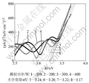
ͼ5 ��Tauc������ϵõ��ĸ���Ĥ�Ĺ�ѧ��϶
Fig.5 Optical band gap of TiO2 thin films prepared at different powers
ͼ6��ʾΪ��ͬ�������Ʊ���TiO2��Ĥ��600 nm���������ʡ���ͼ6���Կ�������ͬ�������Ʊ��ı�Ĥ��������1.8~2.3֮��仯��300 Wʱ�Ʊ��ı�Ĥ��������С��TiO2��Ĥ��������n�뱡Ĥ�ܶ�֮�������µĽ��ƹ�ϵ[17]��
n=0.427 51��+0.919 33 (2)
ʽ�У���Ϊ��Ĥ�ܶȣ�g/cm3�����ʽ(2)���Եó�300 Wʱ�Ʊ��ı�Ĥ���ܶ���ͣ�ͨ�����ܶȵ͵ı�Ĥ����ֲڶȱȽϴ�AFM���пɿ���300 Wʱ�Ʊ��ı�Ĥ����ֲڶ���ߣ����߽���һ�¡�

ͼ6 600 nm����Ĥ�������潦�书�ʵı仯
Fig.6 Variations of refraction index with sputtering power at 600 nm for TiO2 thin films prepared at different powers
3 ����
(1) ���书�ʽϸ�ʱ(��500 W)����Ĥ�������ʽϸߣ��ʽ�������ģʽ��������TiO2��Ĥ�����������书�ʽϵ�ʱ(��500W)����Ĥ�������ʽϵͣ��������ヲ��ģʽ�������ı�Ĥ����
(2) �����书�ʺܵ�(��100 W)ʱ������̬��Ĥ�к���TiO0.5�������ԹⲨ��ǿ�ҵ����գ���ʹ��Ĥ������͡��潦�书����100 W���ӵ�300 W����Ĥ�ı���ֲڶ������ӣ������书�ʽ�һ��������400 Wʱ����Ĥ�ֲڶȷ�����С������ֲڶ�������ɹ��ڱ�Ĥ�����ɢ����ʧ�����DZ�Ĥ���ʽ��͵���Ҫ���ء�
(3) ���书�ʴ�100 W����400 W����õ�TiO2��Ĥ���������Ƚ��ͺ����ӣ�300 Wʱ�Ʊ��ı�Ĥ��������͡���ʵ�������£�400 WΪ�Ʊ����ʸߡ������ʴ��TiO2�����䱡Ĥ�����Ź��ա�
�ο����ף�
[1] Fujibayashi T, Matsui T, Kondo M. Improvement in quantum efficiency of thin film Si solar cells due to the suppression of optical reflectance at transparent conducting oxide/Si interface by TiO2/ZnO antireflection coating[J]. Applied Physics Letters, 2006, 88: 183508.
[2] Bouhafs D, Moussi A, Chikouche A, et al. Design and simulation of antireflection coating systems for optoelectronic devices: Application to silicon solar cells[J]. Solar Energy Materials and Solar Cells, 1998, 52: 79-93.
[3] Zhou W, Tao M, Chen L, et al. Microstructured surface design for omnidirectional antireflection coatings on solar cells[J]. Journal of Applied Physics, 2007, 102: 103105-103113.
[4] Kuo M L, Poxson D J, Kim Y S, et al. Realization of a near-perfect antireflection coating for silicon solar energy utilization[J]. Optics Letters, 2008, 33(21): 2527-2529.
[5] Khelifi S, Burgelman M, Verschraegen J, et al. Impurity photovoltaic effect in GaAs solar cell with two deep impurity levels[J]. Solar Energy Materials and Solar Cells, 2008, 92: 1559-1565.
[6] Richards B S, Rowlands S F, Ueranatasun A, et al. Potential cost reduction of buried-contact solar cells through the use of titanium dioxide thin films[J]. Solar Energy, 2004, 76(1/3): 269-276.
[7] Zribi M, Kanzari M, Rezig B. Structural, morphological and optical properties of thermal annealed TiO thin films[J]. Thin Solid Films, 2008, 516(7): 1476-1479.
[8] ������, �콣, ����ʱ, ��. ϡ����������TiO2��������Ȱ���[J]. ���ϴ�ѧѧ��: ��Ȼ��ѧ��, 2009, 40(1): 139-144.
YIN Li-song, ZHU Jian, WEN Li-shi, et al. Photocatalytic degradation of chloramines phosphorus with RE doped TiO2[J]. Journal of Central South University: Science and Technology, 2009, 40(1): 139-144.
[9] Kim W G, Rhee S W. Effect of post annealing on the resistive switching of TiO2 thin film[J]. Microelectronic Engineering, 2009, 86(11): 2153-2156.
[10] Chen G S, Lee C C, Niu H, et al. Sputter deposition of titanium monoxide and dioxide thin films with controlled properties using optical emission spectroscopy[J]. Thin Solid Films, 2008, 516(23): 8473-8478.
[11] Li Z G, Wu Y X, Miyake S. Metallic sputtering growth of high quality anatase phase TiO2 films by inductively coupled plasma assisted DC reactive magnetron sputtering[J]. Surface and Coatings Technology, 2009, 203(23): 3661-3668.
[12] W?tje K, Ebbecke J, Thorwarth G, et al. Plasma deposition of piezoelectric ZnO layers by rf sputtering, Sol Gel and pulsed laser deposition[J]. Physica Status Solidi C, 2008, 5(4): 943-946.
[13] Bennett H E. Scattering characteristics of optical materials[J]. Optical Engineering, 1978, 17(5): 480-488.
[14] Dannenberg R, Greene P. Reactive sputter deposition of titanium dioxide[J]. Thin Solid Films, 2000, 360(1/2): 122-127.
[15] Ben Amor S, Guedri L, Baud G, et al. Influence of the temperature on the properties of sputtered titanium oxide films[J]. Materials Chemistry and Physics, 2003, 77(3): 903-911.
[16] Zhang M, Lin G Q, Dong C, et al. Amorphous TiO2 films with high refractive index deposited by pulsed bias arc ion plating[J]. Surface and Coatings Technol, 2007, 201(16/17): 7252-7258.
[17] Richards B S. Single-material TiO2 double-layer antireflection coatings[J]. Solar Energy Materials and Solar Cells, 2003, 79(3): 369-390.
(�༭ �°���)
�ո����ڣ�2010-06-05�������ڣ�2010-08-12
������Ŀ������ʡ�ش�Ƽ�ר����Ŀ(08FJ1002)
ͨ�����ߣ��ܼ̳�(1963-)���У����ϳ�ɳ�ˣ����ڣ����µ�����Ϣ�����������о����绰��13873193957��E-mail: jicheng@mail.csu.edu.cn
