

Performance improvement of ZnO film by room-temperature oxygen plasma pretreatment
ZHAO Ping(�� ƽ)1, XIA Yi-ben(���屾)1, WANG Lin-jun(���־�)1, LIU Jian-min(������)1, XU Run(�� ��)1, PENG Hong-yan(������)2, SHI Wei-min(ʷΰ��)1
1.School of Materials Science & Engineering, Shanghai University, Shanghai 200072, China;
2.Physics Department, Mudanjiang Normal College, Mudanjiang 157012, China
Received 10 April 2006; accepted 25 April 2006
Abstract:
The room-temperature oxygen plasma treatment before depositing ZnO films on nanocrystalline diamond substrates was studied. The nanocrystalline diamond substrates were pretreated in oxygen plasma at 50 W for 30 min at room temperature and then ZnO films were sputtered on diamond substrates at 400 W. The X-ray diffraction (XRD) patterns show that the c-axis orientation of ZnO film increases evidently after oxygen plasma pretreatment. The AFM and SEM measurements also show that the high c-axis orientation of ZnO film and the average surface roughness is less than 5 nm. The resistivity of ZnO films increases nearly two orders of magnitude to 1.04��108 ��?cm. As a result, room-temperature oxygen plasma pretreatment is indeed a simple and effective way to improve the performance of ZnO film used in SAW devices by ameliorating the combination between diamond film and ZnO film and also complementing the absence of oxygen atoms in ZnO film.
Key words:
ZnO film; c-axis orientation; nanocrystalline diamond film; oxygen plasma; SAW device;
1 Introduction
For novel application of diamond, the surface acoustic wave (SAW) devices are expected by characteristics of high elastic constant[1, 2]. However, as the SAW is excited in the diamond by electromechanical conversion, a piezoelectric layer such as ZnO or AlN is deposited on the diamond surface. ZnO is a versatile material for many applications due to its structural, electrical and optical properties[3]. It is expected that ZnO thin films with single-crystal quality and high resistivity will provide the highest piezoelectric coupling coefficient and low insertion loss[4].
Previous researches on the growth of ZnO films on diamond films have revealed the importance of the substrate surface during the initial stages of the growth, particularly the lattice mismatch and oxidation of the substrate surface. Some methods, such as growth of ZnO buffer layer[5] and annealing treatment after growth[6], have been tried.
In this study, we report a room-temperature oxygen plasma treatment applied to ZnO film before deposition on the nanocrystalline diamond film. It is found that oxygen plasma pretreatment should be employed in order to obtain ZnO films with good crystallinity and electrical properties.
2 Experimental
The nanocrystalline diamond films, used for ZnO film deposition in this study, were grown on silicon substrates in a hot filament chemical vapor deposition (HFCVD) reactor[7]. The as-grown diamond films had a thickness of 20 ��m determined by SEM cross-section measurements and a polycrystalline structure with a mean surface roughness of 40.8 nm determined from AFM results as shown in Fig.1. Diamond films were subjected to a treatment in the plasma of oxygen at room temperature. The process conditions were a pressure of 0.4 Pa, a radio frequency power of 50 W and a reaction gas of oxygen (99.99%). This was performed in JC500-3/D magnetron sputtering system for 0.5 h. After the plasma treatment, ZnO films were deposited by radio frequency magnetron sputtering method with a ZnO target with a purity of 99.99% and a diameter of 120 mm. The sputtering chamber was evacuated to 3��10-3 Pa before sputtering. During the film deposition, the ambient gas was argon (99.999%). The sputtering power was kept at 400 W in this experiment. All those samples, with or without oxygen plasma pretreatment, have same reaction time as 2 h during the whole process. The thickness of ZnO film was about 600 nm.
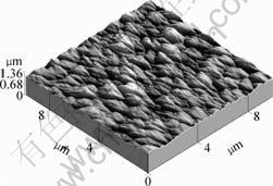
Fig.1 AFM image of nanocrystalline diamond film
The c-axis orientation and crystalline structure were investigated from X-ray diffraction (XRD) (Cu K��, ��= 0.154 056 nm) measurements. The surface morphology was observed by atomic force microscopy (AFM) (AP-0190). The cross-sectional view was observed with field-emission scanning electron microscope (SEM) (JEOL JSM-6700F). The resistivity was measured with semiconductor characterization system (4200-SCS) after depositing electrodes (1 mm in diameter) on ZnO film at room temperature.
3 Results and discussion
The crystalline structure and orientation of the ZnO films were investigated by X-ray diffraction (XRD). Major peak (002)-orientation was identified and compared for ZnO films with and without oxygen plasma pretreatment as shown in Fig.2. The (002) peak increases and FWHM decreases from 0.58 to 0.40 with oxygen plasma pretreatment. This indicates that oxygen plasma pretreatment ameliorates the combination between ZnO film and diamond substrate and makes the c-axis orientation structure develop more easily.
Fig.3 shows a typical AFM image of ZnO film with oxygen plasma pretreatment. The surface roughness is less than 5 nm, and the grain size is about 30 nm. However, with oxygen plasma pretreatment, ZnO films have the same surface roughness and grain size as those without oxygen plasma pretreatment.
Fig.4 shows the scanning electron micrographs of the cross-section for ZnO films with and without oxygen plasma pretreatment. From Fig.4(a), it can be observed
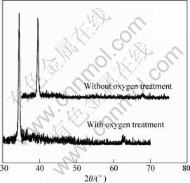
Fig.2 X-ray diffraction patterns of ZnO films with and without oxygen plasma pretreatment
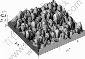
Fig.3 AFM image of ZnO film with oxygen plasma pretreatment
that the film develops a mixture of dense and columnar structure normal to the surface of the substrate, and the surface morphology is textured or ��cratered��. With oxygen plasma pretreatment, columnar structure develops quickly in the vertical direction and the c-axis orientation is observed more obviously, as shown in Fig.4(b). The plasma pretreatment may cause etching of the sp2-bonded carbon impurities in the diamond[8] to provide more smooth diamond surface for growth of ZnO films.
Fig.5 shows the dark-current versus applied voltage (I-V) curves of the ZnO films with and without oxygen plasma pretreatment. It can be calculated that the resistivity of ZnO film increases from 2.04��106 W?cm (without pretreatment) to 1.04��108 W?cm(with pretreatment). As the plasma contains a great number of active particles, such as electrons and ions at high-energy state, molecules and atoms at excited state and free radicals, with an energy range of 0 to 20 eV, the oxygen plasma pretreatment will generate large quantity of free radicals and introduce great amount of oxygen containing base groups onto the surface of diamond substrates[9]. ZnO is an n-type material due to excess zinc in the form of interstitials and oxygen vacancies[10]. In this oxygen plasma pretreatment, the oxygen containing base groups can compensate the oxygen deficiency, thus influencing the resistivity of ZnO films.
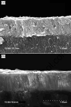
Fig.4 Scanning electron micrographs of cross-section for ZnO film: (a) Without; (b) With oxygen plasma pretreatment
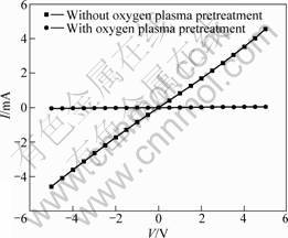
Fig.5 I-V curves of ZnO film with and without oxygen plasma pretreatment
4 Conclusions
The performance of ZnO film was observed by means of XRD patterns, AFM and SEM images and I-V curves. With oxygen plasma pretreatment, the ZnO film deposited on nanocrystalline diamond substrate exhibits higher c-axis orientation. The surface roughness is less than 5 nm and the grain size is 30 nm, which are nearly the same for ZnO film with and without oxygen plasma pretreatment. The resistivity of ZnO films is affected by oxygen plasma pretreatment strongly. The higher resistivity (1.04��108 W?cm) could be obtained for ZnO film with oxygen plasma pretreatment, which is nearly two orders of magnitude larger than that of samples without oxygen plasma pretreatment. Room-temperature oxygen plasma pretreatment improves the properties of ZnO films, especially the crystallinity and electrical properties.
References[1] ELMAZRIA O, MORTET V, HAKIKI M E, NESLADEK M, ALNOT P. High velocity saw using aluminum nitride film on unpolished nucleation side of free-standing CVD diamond[J]. IEEE Transactions on Ultrasonics, Ferroelectrics, and Frequency Control, 2003, 50(6): 710-715.
[2] WU T T, CHEN Y Y. Exact analysis of dispersive saw devices on ZnO/diamond/Si-layered structures[J]. IEEE Transactions on Ultrasonics, Ferroelectrics, and Frequency Control, 2002, 49(3): 142-149.
[3] GORLA C R, EMANETOGLU N W, LIANG S, MAYO W E, LU Y,WRABACK M, SHEN H. Structural, optical, and surface acoustic wave properties of epitaxial ZnO films grown on ![]() sapphire by metalorganic chemical vapor deposition[J]. Journal of Applied Physics, 1999, 85(5): 2595-2602.
sapphire by metalorganic chemical vapor deposition[J]. Journal of Applied Physics, 1999, 85(5): 2595-2602.
[4] EMANETOGLU N W, GORLA C, LIU Y, LIANG S, LU Y. Epitaxial ZnO piezoelectric thin films for saw filters[J]. Materials Science in Semiconductor Processing, 1999, 2(3): 247-252.
[5] YAN J F, LU Y M, LIU Y C, LIANG H W, LI B H, SHEN D Z, ZHANG J Y, FAN X W. Improvement of the crystalline quality of the ZnO epitaxial layer on a low-temperature grown ZnO buffer layer[J]. Journal of Crystal Growth, 2004, 266(4): 505-510.
[6] LIN S S, HUANG J L, SAJGALIK P. The properties of heavily Al-doped ZnO films before and after annealing in the different atmosphere[J]. Surface & Coating Technology, 2004, 185(2): 254-263.
[7] ZHANG M L, XIA Y B, WANG L J, GU B B. Effects of the film microstructures on CVD diamond radiation detectors[J]. Journal of Crystal Growth, 2005, 277(1): 382-387.
[8] WANG S G, SELLIN P J, LOHSTROH A, ZHANG Q. Performance improvement of polycrystalline diamond ultraviolet photodetectors by room-temperature plasma treatment[J]. Applied Physics Letters, 2005, 86: 093503-1-093503-3.
[9] KIM M C, YANG S H, BOO J H, HAN J G. Surface treatment of metals using an atmospheric pressure plasma jet and their surface characteristics[J]. Surface and Coatings Technology, 2003, 174-175: 839-844.
[10] WALTER W, CHU S Y, JUANG Y D, WU S J. Li2CO3-doped ZnO films prepared by RF magnetron sputtering technique for acoustic device application[J]. Materials Letters, 2002, 57(4): 998-1003.
Foundation item: Project(60577040) supported by the National Natural Science Foundation of China; Project(0404) supported by Shanghai Foundation of Applied Materials Research and Development; Projects(0452nm051, 05nm05046) supported by the Nano-technology Project of Shanghai; Project(T0101) supported by Shanghai Leading Academic Disciplines
Corresponding author: WANG Lin-jun; Tel: +86-21-56333514; Fax: +86-21-56332694; E-mail: ljwang@staff.shu.edu.cn
