

Surface treatment of 0.20% C carbon steel by high-current pulsed electron beam
XU Guo-cheng(�����)1, FU Shi-you(��ʯ��)2, GUAN Qing-feng(�����)1
1. Key Laboratory of Automobile Materials, Ministry of Education,
Department of Materials Science and Engineering, Jilin University, Changchun 130025, China;
2. Department of Physics, Weihai Branch, Harbin Institute of Technology, Weihai 264209, China
Received 20 April 2006; accepted 30 June 2006
Abstract:
A high-current pulsed electron beam(HCPEB) generated on the system of Nadezhda-2 was applied to improve the microstructure and performance of 0.20% C low carbon steel. Surface layers of the samples bombarded by explosive electron beam at different pulses was observed by using electron microscopy. The physical model of the thermal-stress process and related modification mechanism as a result of HCPEB irradiation was also investigated. After HCPEB post treatments, obvious changes in microstructure and significant hardening occur in the depth of 200-250 ��m from the surface after HCPEB irradiation. Rapid heating and subsequent rapid solidification induce heavy plastic deformation, which results in that the laminated structure of pearlite is substituted by dispersive rounded-like cementites in the near-surface. The effect of HCPEB treatment can reach more than 500 m depth from the surface. The original crystalline structure is changed to a different degree that grows with the numbers of bombardment, and in the surface layer amorphous states and nanocrystaline structures consisting of grains of ��-phase and cementite are found. The violent stress induced by HCPEB irradiation is the origin of the nanostructured and amorphous structure formation.
Key words:
pulsed electron beam; surface treatment; low carbon steel; microstructure;
1 Introduction
It has been demonstrated[1-5] that the action of a high-current pulsed electron beam(HCPEB) of micro- second duration on metallic alloys in the surface melting mode results in the formation of metastable phase states in the near-surface layer. This is associated with high quenching rates (about 108 K/s) from liquid state of the thin surface (about 0.1-1.0 ��m). This treatment sub- stantially improves the performance of machine parts and tools, for instance, the corrosion resistance of stainless steels and aluminum alloys[2], the wear resistance of cutting tools made of high-speed steel[5] and hard alloys[1, 4] or the fatigue characteristics of titanium alloys[1, 2].
Several physical models and numerical simulations have been developed to show the mechanism of significant structure and property varieties[6-8]. However, their simulation results only partly agree with the experiment results in the surface region, but display a great diversity beyond the depths of the heat-affected zone(HAZ.) In addition, the research on the micro- structures has received less attention compared to numerical simulations, and more efforts should be done for better understanding of the HCPEB modification physical models.
In the present paper, we applied HCPEB technique to irradiate 0.20% C carbon steel. We focued on the microstructures induced by thermal-stress effect generated due to HCPEB irradiation. The physical model of the thermal-stress process and related modification mechanism as a result of HCPEB irradiation was also developed.
2 Experimental
A HCPEB source (Russian-made Nadezhda-2 type) was employed to treat the surface of the 0.20% C low carbon steel. It can produce a pulsed electron beam of low energy (10-40 keV), high peak current (102- 103 A/cm2), short pulse duration (0.5-5 ��s), and high efficiency (repeating pulse interval being 10 s). The electron beam was generated by an explosive emission graphite cathode. Spark plasma sources were placed evenly in a circle behind the anode, providing an anode plasma that conducts the electron beam to the collector (target). An external magnetic field was applied to confine the beam. The accelerating voltage, magnetic field intensity, and anode-collector distance all controlled the beam energy density. More details about the HCPEB system are shown in Refs.[1] and [2].
Annealed 0.20% C steel with composition (mass fraction, %) 0.20C, 0.21Si, 0.34Mn, 0.015P and 0.014S was selected as the target material. Specimens were machined with a size of 14 mm in length, 10 mm in width, 10 mm in height, and one side surface was mirror polished. The polished surfaces of samples were irradiated using this HCPEB system. The HCPEB bombardments were carried out under the following conditions: the electron energy 20-30 keV, current pulsed duration 4.5 ��s, energy density 4 J/cm2, and vacuum 133.322��10-5 Pa. Microstructures were examined with a JSM 5310 scanning electron micro- scopy(SEM) and a H-800 transmission electron micro- scopy(TEM). The thin foils for the TEM observation were obtained by mechanical pre-thinning, dimpling, and electrolytical thinning from the substrate side. Micro- hardness measurements were carried out with an HXD-1000 microhardness instrument.
3 Results and discussion
Fig.1(cross section) represents the SEM morphology of the sample treated by 1 pulse HCPEB irradiation. Other samples with various pulses yield almost uniform morphologic characteristic. It can be found in Fig.1 that along the irradiated surface, there exist an approximately several micrometers wide strip region which is hard to be eroded. The reason for this may be attributed to the melting occurred at this region
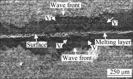
Fig.1 Cross-section SEM morphology of sample treated by 1 pulse HCPEB irradiation (The arrows noted by V indicate the formation of the voids.)
during HCPEB irradiation. Furthermore, because of the quick heat conduction of target bulk, the melted layer was immediately resolidified and a new microstructure layer was formed[3, 9].
Fig.1 also reveals that the obvious changes in microstructure occurred in the depth of 200-250 ��m from the surface after HCPEB irradiation. The wavy boundary paralleled to the surface is formed in the zones. These boundaries are probably the wave front caused by the high tensile strain that attracts the defects[10].
The results of microhardness distribution on the cross-section are shown in Fig.2. It can be seen that the extended hardened zone is present in the near-surface. The microhardness value is higher with multiple-pulses, and the highest microhardness value appears in 5 pulses. Obvious changes in microhardness also occur in the zones from depth of 250 to 500 ��m (even exceeds 500 ��m), in which there are no significant varieties on microstructure in different pulsed numbers. This indicates that the effect of HCPEB treatment can reach more than 500 ��m depth from the surface.
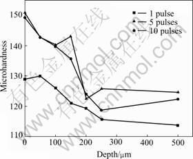
Fig.2 Microhardness distribution on cross-section of samples irradiated with 1, 5 and 10 pulses
It was reported that the heat-affected zone treated by HCPEB was only on the order of ten micrometer, about 10 ��m[9]. This indicates that there must be another effect contributing to the HCPEB treatment of samples. It may be the stress wave effect[10], which was induced by flash heating of HCPEB to target surface, and the stress wave may be strengthened or even transformed to shock wave in some regions of the target in its propagation process. There are two sources for the generation of the stress waves. The first is thermal expansion inside steep temperature field in the surface layer. The second is caused by eruption of surface materials after over heating to evaporation, leaving crater-like surface[3, 6-9]. The stress wave should be responsible for the increases of microhardness in the deeper region of samples irradiated by HCPEB even if no obvious microstructure changes were found by SEM investigation.
Fig.3 illustrates the cross-section SEM morpho- logies of the samples before and after HCPEB irradiation. Fig.3(a) shows that the original 0.20% C low carbon steel possesses ��-ferrite and pearlite dual phase microstructure. After 1 pulse irradiation, the laminated structure of pearlite vanishes in the zones approximately 50 ��m instead of a few rounded-like cementites precipitate at the grain boundaries of ��-ferrite, as shown in Fig.3(b). After 5 and 10 pulses irradiation, it shows good dispersion of well-rounded cementites approximately 1 ��m size in the ��-ferrite matrix in the near-surface, as shown in Figs.3(c) and 3(d). The rounded cementites which look like to be broken were observed even in the zones about 150-200 ��m from the surface. Obviously, the rounded cementites in the deeper zones from irradiated surface originate from the stress waves and they may have higher hardness.
PROSKUROVSKY et al[2] believed that the thermal stress wave induced by HCPEB treatment was the dominant factor for the structure and property varieties beyond the HAZ. They described the thermal stress wave in Fe induced by the HCPEB treatment using numerical simulations. The amplitude of the simulated thermal stress wave is as weak as 0.1 MPa, too low to manifest the significant structure and property modifications.
Due to the drastic temperature change, a steep temperature gradient is generated along the incident direction of the beam. However, due to the lateral confinement along the surface, the thermal expansion in the directions vertical to the beam is strongly resisted, causing the quasi-static thermal stress ��y, as shown in Fig.4(a), and the thermoelastic stress wave (��x) is also shown. As the temperature rises, a local melting starts in a subsurface layer[2, 7-9]. Therefore, the locally melted droplets are formed beneath the surface as shown in Fig.4(b). Due to the liquid pressure, a resultant force p from the quasi-static thermal stress and the liquid volume expanding exerts on the droplets and is transmitted by the droplets in all directions. The force p along the beam direction constitutes the source of the shock thermal stress wave (Fig.4(b)). It is then enhanced by the increasing temperature, as schematically represented as a wave oscillation in Fig.4(b). If the thin outer surface solid layer cannot withstand this pressure, a volcano-like eruption occurs as shown in Fig.4(c). The shock stress is then released (Fig.4(c)). After the eruption, the compressive stress is then released, as described in Fig.4(c). The maximum compressive quasi-static stress p in the surface layer, according to the numerical simulation developed by ZOU et al[7], can reach several
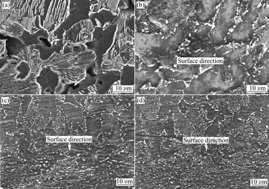
Fig.3 SEM morphologies of cross-section before and after HCPEB irradiation: (a) Unirradiated; (b) 1 pulse; (c) 5 pulses; (d) 10 pulses
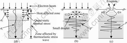
Fig.4 Schematic illustration of crater formation by means of eruption from sub-layer and shock thermal stress induced by HCPEB bombardment
hundreds of MPa, which easily induces violent deformation in metallic materials, causing significant structure and property modifications.
In this study the observation indicates that the microstructures of target greatly affect the propagation process of the stress wave. Fig.1 reveals that many voids indicated by the arrows marked with ��V�� show approximately 0.05-0.1mm beneath the surface. They decrease the propagation distance of the wave, whereas the wave propagation is deeper in the regions without voids.
It is worth noting that after multi-pulses, the nanometer-size austenite and cementite precipitates in the ��-ferrite matrix were observed in the near-surface, as shown in Fig.5(a). After 10-pulsed, an amorphous structure is even massively formed in the 0.20% C carbon steel, as shown in Fig.5(b). It is believed that amorphization of the Fe-C alloys has never been achieved by rapid quenching as far as we know. Thus, the rapid solidification seems not to be the only reason for the formation of the amorphous phase during HCPEB treatments, although the quenching rate could reach 108 K/s. Obviously, the formation of the nanostructure and the amorphous structures may be a close implication with the violent stress induced by HCPEB irradiation.
4 ConclusionsAfter HCPEB post treatments, obvious changes in microstructure and significant hardening occur in the depth of 200-250 ��m from the surface after HCPEB irradiation. The laminated structures of pearlite are substituted by dispersive rounded-like cementites in the near-surface. The effect of HCPEB treatment can reach more than 500 ��m of depth from the surface. Rapid heating and subsequent rapid solidification induce heavy plastic deformation. After multi-pulse bombardments, both austenite and cementite type of nanostructure par-
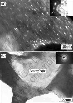
Fig.5 (a) TEM dark field image of nanograined cementite and austenite in ferrite matrix of sample treated by 5 pulses at 4 J/cm2; (b) TEM bright field image of amorphous structure of sample treated by 10 pulses at 4 J/cm
ticles are formed from the supersaturated Fe(C) solid solution phase. After 10 pulses, the amorphous structure is formed in the local zones. The violent stress induced by HCPEB irradiation is the origin of the nanostructure and amorphous structure formation.
References[1] PROSKUROVSKY D I, ROTSHTEIN V P, OZUR G E, IVAMOV YU F, MARKOV A B. Physical foundations for surface treatment of materials with low energy, high current electron beams [J]. Surface and Coatings Technology, 2000, 125: 49-56.
[2] PROSKUROVSKY D I, ROTSHTEIN V P ,OZUR G E, MARKOV A B, NAZAROV D S. Pulsed electron-beam technology for surface modification of metallic materials [J]. J Vac Sci Technol A, 1998, 16: 2480-2488.
[3] GUAN Q F, ZOU H, ZOU G T, WU A M, HAO S Z, ZOU J X, QIN Y, DONG C, ZHANG Q Y. Surface nanostructure and amorphous, state of a low carbon steel induced by high-current pulsed electron beam [J]. Surface and Coatings Technology, 2005, 196: 145-149.
[4] POGREBNJAK A D, SHUMAKOVA N I. Effect of ��duplex�� treatment on changes of physical and mechanical proerties of steel (0.3 wt% C) [J]. Surf Coat Tech, 1999, 122: 183-187.
[5] IVANOV Y F, ROTSHTEIN V P, PROSKUROVSKY D I, ORLOV P V, POLESTCHENKO K N, OZUR G E, GONCHARENKO I M. Pulsed electron-beam treat of WC-TiC-Co hard alloy cutting tools: wear resistance and microstructure evolution [J]. Surf Coat Tech, 2000, 125: 251-256.
[6] MARKOV A B, ROTSHTEIN V P. Calculation and experimental determination of dimensions of hardening and tempering zones in quenched U7A steel irradiated with a pulsed electron beam [J]. Nucl Instr and Meth B, 1997, 132: 79-86.
[7] ZOU Jian-xin, QIN Ying, DONG Chuang, WANG Xiao-gang, WU Ai-min, HAO Sheng-zhi. Numerical simulation of thermal- mechanical process during high current pulsed electron beam (HCPEB) treatment [J]. J Vac Sci Technol A, 2004, 22: 545-552.
[8] QIN Y, ZOU J X, DONG C, WANG X G, WU A M, LIU Y, HAO S Z, GUAN Q F. Temperature-stress fields and related phenomena induced by a high current pulsed electron beam [J]. Nucl Instrum Methods Phys Res B, 2004, 225: 544-554.
[9] GUAN Q F, YANG P L, ZOU H, ZOU G T. Nanocrystalline and amorphous surface structure of 0.45%C steel produced by high current pulsed electron beam [J]. J Mater Sci, 2006, 41: 479-483.
[10] DONG C, WU A M, HAO S Z, ZOU J X. Surface treatment by high current pulsed electron beam [J]. Surf Coat Technol, 2003, 163-164: 620-624.
Corresponding author: GUAN Qing-feng; Tel: +86-431-5095326; Fax: +86-431-5094994; E-mail: guanqingfeng@jlu.edu.cn
