
Dislocation of Cz-sapphire substrate for GaN growth by chemical etching method
NIU Xin-huan(ţ�»�) 1, LU Guo-qi(¬����)2, ZHANG Wei-lian(��ά��)2,
GAO Jin-yong(�߽�Ӻ)1��LIU Yu-ling(������)1
1. School of Information Engineering, Hebei University of Technology, Tianjin 300130, China;
2. School of Materials, Hebei University of Technology, Tianjin 300130, China
Received 10 April 2006; accepted 25 April 2006
Abstract:
The diameter of Czochralski (Cz) sapphire crystals is 50 mm. The sapphire substrates were lapped by using diamond powders and polished by chemical mechanical polishing(CMP) method using alkali slurry with SiO2 abrasive. After obtaining the smooth surfaces, the chemical etching experiments were processed by using fused KOH and NaOH etchants at different temperature for different times. The dislocation was observed by means of optical microscope and scanning electron microscope. The clear and stable contrast images of sample etching pits were observed. On the whole, the dislocation density is about 104-105 cm-2. Comparing the results under the conditions of different etchants, temperatures and times during the etching proceeding, it was found that the optimal condition for dislocation displaying is etching 15 min with fused KOH at 290 ��. At the same time, the formation of the etch pits and the reducing method of dislocation density were also discussed.
Key words:
sapphire; single crystal; dislocation; chemical etching; metallograph; KOH and NaOH etchant; Czochralski;
1 Introduction
Sapphire (��-Al2O3) has a hexagonal structure and belongs to D6 3d R3mC space group, a=b=0.478 5 nm, c=1.288 1 nm. Its melting point is as high as 2 333 K, and it can be obtained through several techniques, including TGT method[1], EFG and GES methods[2-4], HEM method[5,6], and Cz method[7]. Sapphire single crystal combines many good mechanical and optical properties [4,6] that make it become the choice of material in a variety of modern Hi-Tech applications such as space and military optical systems, high-power laser optics and high-pressure components. In addition, the (0001) sapphire crystal wafers can be used as substrates for growing photoelectric materials-GaN thin films[8]. Sapphire wafer is also widely used for GaN-based ��-nitride device fabrication[9]. However, sapphire wafer is known to be difficult for other processing such as etching and device separation using mechanical cutting or scribing due to the high chemical and thermal stability, high hardness, and the differences of the crystal orientation between GaN with sapphire [10].
Different applied fields require different crystal quality, and the intrinsic quality, crystal defect and impurity concentration of sapphire crystal can influence the quality of the epitaxial layer and devices directly. So, for preparing high quality crystal it is very important to display the dislocation clearly and study its formation mechanics. In this study, the (0001) crystal grown by Cz method was used. To characterize the imperfection of the crystal, optical microscopy, chemical etching (KOH and NaOH etchant) and SEM were adopted. The condition of displaying the crystal dislocation and the formation of etch pits were also discussed. The optimal processing was got for Cz-sapphire crystal chemical etching, which was not seen before.
2 Experimental
In this study, the sapphire crystals were obtained by Czochralski (Cz) method. The diameter is 50 mm. The crystals were grown by using a [0001] direction seed under a high pure flowing argon gas atmosphere with a pulling rate of 1.5-2 mm/h and a rotation rate of 10-30 r/min.
After being edge rounded, sapphire crystal wafers with thickness of 1.0 mm for test were cut perpendicular
to the growth direction from the equant section of crystal-bar. The surfaces were lapped using diamond powders and polished by CMP(chemical mechanical polishing) method using alkali slurry with SiO2 abrasive. After obtaining the smooth surfaces, the chemical etching experiments were processed by using fused KOH and NaOH etchants at different temperatures for different times. Then, the etched sample was cooled and washed with ultrasonic wave and dried in air. The dislocation was observed by means of optical microscope and PHILIPS XL30W/TMP SEM method.
3.1 Chemical etching by fused KOH and NaOH
The chemical reaction is very difficult between sapphire and acid or alkali at room temperature. But the fused KOH and NaOH can etch sapphire single crystal at high temperature.
First, the prepared sapphire was etched by fused KOH for 10 min at different temperatures. When the temperature reached 160 ��, the etch pits appeared and the dislocation density was 0.5��104 cm-2(Fig.1). When the temperature reached higher than 260 ��, the dislocation density was nearly unchanged(Fig.2). So we chose 290 �� as the experiment temperature.
Table 1 shows the dislocation density of sapphire etched by fused KOH at 290 �� for different times. Fig.3 shows the metallographs of sapphire etched by fused KOH at 290 �� for different times.
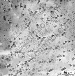
Fig.1 Metallograph of sapphire etched by fused KOH at 160 �� for 15 min
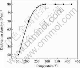
Fig.2 Dislocation density of sapphire etched by fused KOH at different temperature for 10 min
Table 1 Chemical etching of sapphire

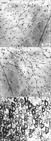
Fig.3 Metallographs of sapphire etched by fused KOH at 290 �� for different times: (a) 10 min; (b) 15 min; (c) 20 min
Fig.4 shows the SEM image of single etch pit and Fig.5 shows the SEM image of sapphire etched for 15 min.
From Fig.3, we can see that contrast image of sapphire etch pits is more clear and stable at 290 �� for 15 min than for 10 and 20 min.
Using the same method, we etched the prepared sapphire by fused NaOH at different conditions, and found the condition of displaying the clear and stable contrast image of etch pits was at 320 �� for 30 min. From Fig.3(b) and Fig.6, it is easy to find that the contrast image of etch pits is more clear and stable in Fig.3(b). So we choose fused KOH at 290 �� for 15 min as the optimal etching condition.
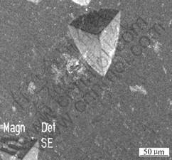
Fig.4 SEM image of single etch pit

Fig.5 SEM image of sapphire etched for 15 min
3.2 Formation mechanism of etch pit
It is well known that the shape of dislocation etch pits reflects the structural symmetry of sapphire crystals. To interpret the shape of the etch pits of (0001) sapphire slice, a schematic figure of the planar structure of (0001) sapphire crystal face is shown in Fig.7[11], from which we can investigate the
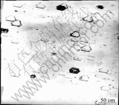
Fig.6 Metallograph of sapphire etched by NaOH at 320 �� for 30 min
formation of different etch pits in the (0001) face. The etchant has an effect of attacking the chemical bond between molecules or atoms, and those weaker bonds such as those between the same O2- ions are always being destroyed first, which results in forming a certain etch pit pattern. From Fig. 7, therefore, it is not difficult to understand why it is easy to generate the triangular, hexagonal, and quadrilateral shapes of etch pits in (0001) sapphire crystal faces.
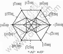
Fig.7 Schematic figure of planar structure of (0001) sapphire crystal face
During the crystal growth, the forming site of dislocation is always on the weaker bonds between molecules or atoms. And the crystal defect is always in higher energy, unstable and non-equilibrium state. During the chemical etching process, the crystal lattice atoms at defect first react with etchant and delivery energy to be up to equilibrium state. Then, some etch pit images with specific shape appear. If the etching time is not longer enough, the reaction is not complete, the weaker chemical bond can��t be broken completely and the dislocation contrast image is not enough clear and stable(Fig.3(a)). If the etching time is much longer, the etchant can also etch the integral crystal lattice except the defect, then the dislocation displaying is shielded partly (Fig.3(c)), which influences the effect of observation.
3.3 Formation of dislocation and reducing of dislocation density
In the process of practical crystal growth, in order to assure the Al2O3 melting temperature and normal crystal growth temperature, the designing of thermal field is packaged. So external condition fluctuations always induce the unstable variation of temperature gradient. Sometimes, for practical crystal growth, the diameter ratio of crucible and crystal is unreasonable (such as using d 80 mm crucible for d 50 mm crystal growth), which can induce greater temperature gradient. In addition, the irregular thermal convection in melt induces the microfluctuation of crystal growth rate, which influences the crystal integrity. So there is still no dislocation-free sapphire crystal in the world. In order to decrease sapphire crystal defect, the important aspect is to oversize the crucible diameter properly and control the appropriate diameter ratio of crucible and crystal. Through improving the present thermal field design, the sapphire crystal dislocation density may be decreased.
4 Conclusions
The dislocation in Cz-sapphire crystal(��-Al2O3) with diameter of 50 mm was observed by chemical etching-optical microscopy and SEM methods. The clear and stable contrast images of sample etching pits were observed. On the whole, the dislocation density was about 104-105 cm-2. Comparing the results under the condition of different etchants, temperatures and times during the etching proceeding, we found the optimal condition for dislocation displaying was etching 15 min with fused KOH at 290 ��. Under the condition of etchant etching, the formation of the etch pits was related with crystal bonds strength and the state of crystal defect. The formation reason of dislocation was related with thermal field, diameter ratio of crucible and crystal, temperature gradient and thermal convection in melt during the crystal growth.
References
[1] ZHOU G, XU J, DENG P, XU K, et al. The chemical etching dislocation topographes analysis of Al2O3 sapphire(d 110 mm��80 mm) grown by TGT[J]. J Synth Crystals, 1999, 27: 727-733.(in Chinese)
[2] BUNOIU O, NICOARA I, SANTAILLER J L, et al. Fluid ?ow and solute segregation in EFG crystal growth process[J]. Journal of Crystal Growth, 2005, 275: 799-805.
[3] KRYMOY V M, KURLOV V N, ANYONOV P I, et al. Temperature distribution near the interface in sapphire crystals grown by EFG and GES methods[J]. Journal of Crystal Growth, 1999, 198/199: 210-214.
[4] KURLOV V N, EPELBAUM B M. EFG growth of sapphire tubes up to 85 mm in diameter[J]. Journal of Crystal Growth, 1998, 187: 107-110.
[5] CHEN W M, MCNALLY P J, SHVYD��KO Y V, et al. Dislocation analysis for heat-exchanger method grown sapphire with white beam synchrotron X-ray topography[J]. Journal of Crystal Growth, 2003, 252: 113-119.
[6] CHEN JYH-CHEN, LU CH W. Influence of the crucible geometry on the shape of the melt-crystal interface during growth of sapphire crystal using a heat exchanger method[J]. Journal of Crystal Growth, 2004, 266: 239-245.
[7] XIAO J Z H, YIN S H T, SHAO M J, et al. Observation of dislocation etch pits in a sapphire crystal grown by Cz method using environmental SEM [J]. Journal of Crystal Growth, 2004, 266: 519-522.
[8] NELTON W A, PANKOVE J I. GaN growth on sapphire[J]. Journal of Crystal Growth, 1997, 178: 168-172.
[9] HSU Y P, CHANG S J, SU Y K. ICP etching of sapphire substrates[J]. Optical Materials, 2005, 27: 1171-1174.
[10] KIM DW, JEONG C H, KIM K N. High rate sapphire (Al2O3 ) etching in inductively coupled plasmas using axial external magnetic field[J]. Thin Solid Films, 2003, 435: 242-246.
[11] XIAO Jing-zhong, YIN Shao-tang, et al. Observation of dislocation etch pits in a sapphire crystal grown by Cz method using environmental SEM[J]. Journal of Crystal Growth, 2004, 266: 519-522.
Foundation item: Project(59772037) supported by the National Natural Science Foundation of China; project(500016) supported by the Hebei Natural Science Foundation; Project(20050080007) supported by the Specialized Research Fund for the Doctoral Program of Higher Education of China
Correspondence: NIU Xin-huan; Tel : +86-22-26564424, E-mail : xingguojia@eyou.com


