
���±�ţ�1004-0609(2007)03-0410-07
SnCuǥ�϶Ʋ���Cu/Ni�Ʋ�ǥ����ͷ�Ľ��淴Ӧ
�� �ۣ������࣬�����壬���죬���
(��������ҵ��ѧ ���Ͽ�ѧ�빤��ѧԺ �����о��ң������� 150001)
ժ Ҫ��
�۲��˲�ͬ���ӹ���������ǥ����ͷ������۽ṹ������ǥ�������еĽ��淴Ӧ���з�����̽����ǥ����洦IMC���������ƣ�ͨ���Բ�ͬǥ���¶Ⱥͱ���ʱ���µ�IMC�������ɵķ�������ͭ�������������¶Ⱥ�ʱ��Ĺ�ϵ���̡����������ǥ��������SnCuǥ�ϺϽ�Ʋ���ɺ���Cu��Ľ��洦���ɽ����仯����Cu6Sn5��Cu3Sn�����������������뺸��ʱ��֮�����������߹�ϵ�����������������Ϊ��ɢ��Ӧ���ƹ��̣����溸��ʱ����ӳ�������������������½���
�ؼ��ʣ�
SnCuǥ�϶Ʋ���Cu/Ni�Ʋ��������仯������ǥ�������淴Ӧ��
��ͼ����ţ�TG 111���� ���ױ�ʶ�룺A
Interfacial reactions between Sn-Cu solder alloy and Cu/Ni coatings during reflow soldering
DIAO Hui, WANG Chun-qing, ZHAO Zhen-qing, TIAN Yan-hong, KONG Ling-chao
(Microjoining Laboratory, School of Materials Science and Engineering,
Harbin Institute of Technology, Harbin 150001, China)
Abstract: The interface microstructures of soldered joints under different soldering techniques were observed and analyzed. The interface reaction during soldering was studied. The growth mechanism of the IMCs was discussed and the influences of soldering temperature and dwell time on IMC evolution were investigated. The equation of the relationship between IMCs thickness and soldering conditions including soldering temperature and dwell time was developed. The results suggest that��during soldering, the joint interface between the solder and Cu/Ni coating exhibits a duplex structure of Cu6Sn5 and Cu3Sn intermetallic compounds (IMCs). A parabolic relationship exists between the growth of the IMC layer and soldering time. This indicates that the mechanism of IMC growth is a diffusion-controlled process. The growth rates for the intermetallic layers increase with soldering temperature, whereas decreases with time.
Key words: SnCu solder alloy coating; Cu/Ni coating; intermetallic compound; soldering; interfacial reaction
���ӷ�װ��С�͡���㡢���ܶȡ��߿ɿ��Ե�Ҫ���µ��۷�װ������Ѹ�ٷ�չ���⼫��������˵��Ӳ�Ʒ�д��ʡ����١�С�ͻ������ƣ�������۷�װ�ڼ��ɵ�·�ķ�װ������ռ��������Ҫ�ĵ�λ[1-4]��
��ʵ����õ�Ƽ�����Ni���ɲ㡢�ɺ���Cu��Ԥ�������Ͻ���棬��Cu�������SnCuǥ�ϺϽ�Ʋ�[5-6]����ǥ����������SnCuǥ��/Cu�Ʋ��ͷ���洦���ɽ����仯������ڽ����仯���������Ӳ������ԣ�������Ƚ�Сʱ������ǥ�Ϻ�����֮��ʵ�ֽϺõ�ұ�����ӣ����ǻ�����Ĺ�������������Ӱ���ͷ������[7-9]���Խ����仯������γɻ��Ƽ�Ӱ�����ص��˽⽫�����ڿ����������ͷֲ���������нϴ��ʵ�����塣
1 ʵ��
��Ʋ���ֱ����ˢ�Ƶ�Դ��ͨ�������·�еİ���Сʱ�Ƽ�����ˢ�ƹ��������ĵĵ���ʵ�ֶԶƲ��ȵĿ��ơ�ǥ��ʵ���豸Ϊ�ȷ������������¿ؾ���Ϊ��1 �档
�������徭���͡���ʴ�����⡢��п�ȶ�ǰԤ���������Ժ������ڱ����϶Ƹ�Ni�㡢Cu���Լ�SnCuǥ�ϺϽ�Ʋ㡣���õĶƲ�ṹ��ͼ1��ʾ��

ͼ1 �Ʋ�ṹʾ��ͼ
Fig.1 Schematic plans of brush plating layers: (a) Before soldering; (b) After soldering
ˢ����ɺ��Լ������ȷ�������¯�н���ǥ��ʵ�顣�ڵ��ں����¶�40~60 ���������Ԥ��15~30 s����(300��2) �桢(340��2) �桢(380��2) ���·ֱ���0.5��2��5��10��15��20 min����������£���ȴ����Ϊ3~10 ��/s��
2 ��������
ͼ2��ʾΪCu-SnCu���洦�ֲ��Ŵ��SEM��Ƭ����ͼ�ɿ�����Cu����SnCu�Ͻ�Ʋ���洦����һ��Լ1 ��m�Ľ�ϲ㡣
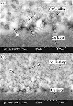
ͼ2 Cu-SnCu���洦�ֲ��Ŵ�SEM��Ƭ
Fig.2 Partially enlarged drawings of Cu-SnCu joint interface
ͼ3��ʾΪCu-SnCu ��Ͻ��洦�����������������ֱ�ڶƲ㷽���ϵ��SnCu�Ͻ�ijɷֳʹ����Ա仯��Cu-SnCu����洦��a����Cu����Ϊ57.61%(������������ͬ)�����ŵ�����Ľ��У��Ͻ�Ʋ��е�Cu�������١���b��Cu����Ϊ45.83%�������cʱ��Cu��������21.42%����Cu-SnCu ����洦���ϺϽ�Ʋ�Ļ������Ͻ���Cu��SnԪ�س����ĺ����ﵽһ���ȶ�״̬�����кϽ�����н����������d��Cu����Ϊ9.51%���ϰ�����e��Cu����Ϊ5.57%��
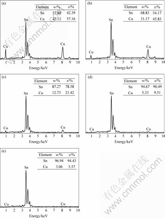
ͼ3 Cu-SnCu���洦EDX����
Fig.3 EDX analysis of Cu-SnCu joint interface: (a) Spot a in Fig.2; (b) Spot b in Fig.2; (c) Spot c in Fig.2; (d) Spot d in Fig.2; (e) Spot e in Fig.2
�ںϽ��Һ�У����ڽ�����������������/��Һ�����ϣ��������������Ũ���Ǿ��������Ͻ���ɵ�����Ҫ���ء���ɢ�������ڵ�����Ͻ�Ļ�������Ϊ[10]

���ڲ��Ͻṹ�������Ժ����Ե�ƥ�䣬�Ͻ���Һ�е�Cu�����ȳ�����Cu��ı��棬SnԪ����Գ����������٣�������Һ��Cu���ӵ�Ũ���½������ŵ�����Ľ��У���Һ����Һ/�������洦Cu���ӵ�Ũ���ݶȼ�С���ȳ����ĶƲ�ṹ�����ı䣬Cu���ȳ����Ķ������ͣ�Cu��Sn�Ĺ������ﵽһ���ȶ�״̬����˳���Cu-SnCu���洦��Ʋ������Cu�������ٲ������ȶ���һ�ֹ���״̬��
��ǥ�������У� SnCu�Ʋ��ۻ���ΪҺ̬ǥ�ϣ��ڹ�Һ��������Ϸ���ԭ�����������Cuԭ�ӵ��ܽ⣬Cu���Ե�γ�Cu�ĸ����������ֲ�����Cu�����ﵽCu��Һ̬Sn�е��ܽ⼫��ʱ��CuԪ�ؼ��Խ����仯�������ʽ���������Թ����Cu��Ϊ����ᾧ������
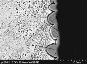
ͼ4��ʾΪ����ʱ��Ϊ2 min�ĺ���SEM��Ƭ�����洦�ֲ��Ŵ��SEM��Ƭ������Cu����ǥ�ϵĽ��洦��������������仯�����ͼ5��ʾ����EDX�������(ͼ6)��֪�ȱ�״���������ΪCu6Sn5��Cu6Sn5��Cu��֮��ı���״������ΪCu3Sn��

ͼ4 �����SEM������Ƭ
Fig.4 Cross-sectional microstructures of joints soldered at different temperatures and time: (a) 300 ��, 2 min; (b) 340 ��, 2 min; (c) 380 ��, 2 min
ͼ5 ������洦�ֲ��Ŵ�SEM��Ƭ
Fig.5 Partically enlarged SEM image of soldered joint

ͼ6 ���洦������EDX�ɷַ���
Fig.6 EDX analysis of IMCs of Cu-SnCu joint interface: (a) Spot a in Fig.5; (b) Spot b in Fig.5
Cu6Sn5������Ϊ��������ṹ����ͬ���᷽����Cu6Sn5�������ʲ�ͬ[9]�����Cu6Sn5������������ȱ�״��ǥ���ڲ����������ȱ�״���������֮�䣬���������Cu�Ʋ�İ��ۡ�����Cu��Һ̬Sn�е���ɢ����Ϊ17.5 kJ/mol����Cu3Sn���е���ɢ����Ϊ65 kJ/mol[11]����ˣ���Щ������Cuԭ����Cu6Sn5�����������ǥ�Ͻ��洦��ɢ�Ŀ���ͨ����Cuԭ���ڰ��۵ײ��ܽ����Һ̬ǥ���У�������ɢ���ȱ�״������ǥ�ϵĽ��洦��Sn��Ӧ����Cu6Sn5����Cu6Sn5���������У�����ʱ���ӳ��������ᄃ���ֻ�������
���ھ����뾶Ϊr�İ����壬����Gibbs-ThomsonЧӦ���ھ������洦����ԭ��(Cu)��Ũ��crΪ
![]()
���ڻ��������ʰ뾶��ͬ�����µ�����ԭ��ͨ��Ϊ��
��ʽ(5)���Կ������ڽ����仯�������������У��ȱ�״�����γɺ��Ѿ��γɵľ����ں���(��ֱ�ڻ�������������)�Ĵֻ�����ȡ���ڴֻ�ͨ��J��ϵ��![]() �е�3�����أ���ɢϵ��D��ǥ���¶�T������Cu��Һ̬ǥ���еı����ܽ��c0������Cu��Һ̬ǥ���е���ɢϵ�����¶ȵ�Ӱ���С��ԼΪ10-5 cm2/s����ˣ�Cu6Sn5�ĺ���ֻ�������Ҫȡ����ǥ���¶�T������Cu��Һ̬Sn�еı����ܽ��c0��
�е�3�����أ���ɢϵ��D��ǥ���¶�T������Cu��Һ̬ǥ���еı����ܽ��c0������Cu��Һ̬ǥ���е���ɢϵ�����¶ȵ�Ӱ���С��ԼΪ10-5 cm2/s����ˣ�Cu6Sn5�ĺ���ֻ�������Ҫȡ����ǥ���¶�T������Cu��Һ̬Sn�еı����ܽ��c0��
���ɵ�Cu6Sn5���������Cu�Ʋ����һ����ɢż����Ԫ��Ũ���ݶ��������������£�Cu����Cu6Sn5���洦����Ԫ�ص����ɢ��������ɢ���̵Ľ��У�������Ԫ�شﵽһ��Ũ�����ʱ������Cu3Sn����ʽ������Cu3Sn����������������˲�״����ʽ������
Ϊ�˶����������洦�����仯������������ɣ��ֱ������ͬ����ʱ�����������ֻ������������ȡ�
��ǥ����������һ����Cu6Sn5��Cu��Ӧ����Cu3Sn�������ģ����ֱ�Ӳ������õ�Cu6Sn5�ĺ��ֵ��ʵ�����ɵ�Cu6Sn5�ĺ��ֵ֮����ƫ�Ӧ�Բ������õ�Cu6Sn5���ֵ������������[12-13]��

����������Ļ�����������ݣ�������ͬǥ���¶�������Cu3Sn��Cu6Sn5���������ʱ��Ĺ�ϵ���ߣ������ͼ7��ʾ��
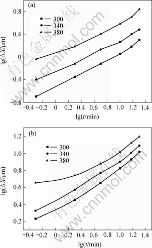
ͼ7 ���������������
Fig.7 Growth curves of intermetallic compounds from 300 �� to 380 ��: (a) Cu3Sn phase; (b) Cu6Sn5 phase
����������ϵõ���ͬ�¶�ʱCu3Sn���������̷ֱ���ʽ(9)~(11)��ʾ��
300 ��ʱ
![]()
340 ��ʱ
![]()
380 ��ʱ
![]()
��Cu6Sn5������������ʽ(12)~(14)��ʾ��
300 ��ʱ
![]()
340 ��ʱ
![]()
380 ��ʱ
![]()
�����Ϸ�����֪�������仯��������������ʱ��Ĺ�ϵ��ѭ�����߶��ɣ�Ϊ��ɢ���̿��Ʒ�������Ӧ[14-15]������
���������������̶�ʱ���������õ�Cu3Sn��Cu6Sn5��˲ʱ�������ʣ������ͼ8��ʾ��Cu3Sn��λ��Cu���Cu6Sn5�������֮�䣬����������������Ԫ��֮��Ĺ�����ɢ��������ɢ���¶Ⱥ�ʱ��Ŀ��ƣ��¶Ⱦ�����ɢ���ʣ���һ���¶����ӳ�����ʱ�����������ɢ������ͼ8(a)�ɿ����¶Ⱥ�ʱ���Cu3Sn������Ӱ�졣���ź���ʱ������ӣ����������������ɢ���������ʱ���ӳ���Cu3Sn�������������½��������¶����ӿ���ԭ�ӵ���ɢ���ʣ���Cu3Sn���������дٽ����á�
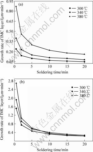
ͼ8 �������˲ʱ��������
Fig.8 Growth rates of intermetallic compound layer: (a) Cu3Sn layer; (b) Cu6Sn5 layer
��ͼ8(b)�ɿ�����ǥ���¶�һ��ʱ�����ź���ʱ������ӣ�Cu6Sn5�������������½�����������Cu6Sn5�������������ʱ�������������Cu���е�Cuԭ����ɢ·�̼Ӵ�ʹ��Cu6Sn5�����������½���Cu6Sn5����������Ĵֻ�����ʹ��Cuԭ�ӵĿ�����ɢͨ���������ܶȼ�С��Ҳ�ή��Cu6Sn5���������ʡ�
ǥ��ʱ��С��2 minʱ��Cu6Sn5��������Ƚ�С���ȱ�״���������֮�䰼�۵��ܶȽϴ��¶����ӿ���ԭ�ӵ���ɢ���ʣ��ٽ���Cu6Sn5������������ǥ��ʱ������ӣ�Cu6Sn5�ȱ�״����������������ԵĴֻ����������¶�Խ�ߴֻ�ͨ��Խ�����ܶȵļ����½�������Cu6Sn5���������ʣ��Ի�������������������ã�ǥ���¶����߶Ի�������������дٽ����á��ڶ��ߵĹ�ͬ�����£�ǥ��ʱ��С��5 minʱ��������������������¶����߶��������ӡ���ǥ��ʱ�䳬��5 minʱ��380 ����Cu6Sn5���������֮��İ��ۻ�����ʧ���ֻ��������������ô����¶����ߵĴٽ����ã�ʹ��Cu6Sn5���������ʿ�ʼС�� 340 ��ʱ���������ʡ�
3 ����
1) SnCuǥ�ϺϽ�Ʋ���Cu�Ʋ�ǥ����ͷ���洦���ɵĽ����仯����ֱ�ΪCu6Sn5��Cu3Sn��Cu6Sn5������������ȱ�״��ǥ���ڲ�������Cu3Sn�����������������״����ʽ������
2) �����仯���������ǥ��ʱ��֮����������߹�ϵ������ǥ�������н����仯���������Ϊ��ɢ���Ʒ�Ӧ��
3) Cu3SnΪ������ɢ���Ʒ�Ӧ�������¶����ߣ�ԭ�ӵ���ɢ���ʼӿ�ٽ��������������ǥ��ʱ�����ӣ��������������ԭ�ӵ���ɢ·�������������˻�������������ʡ�
4) ����ԭ����ɢ·�̵������ͻ���������Ĵֻ�������ͬӰ����Cu6Sn5���������ʡ������¶���300 �����ߵ�340 ��ʱ��Cu6Sn5�������������¶����߶��������ӡ�380 ��������ǥ��ʱ��ӽ�10 minʱ��Cu6Sn5����������С��340 ��ʱ���������ʡ�
REFERENCES
[1] Bhatgadde L G, Joseph S, Kulkarni S C. Electroless copper/nickel/gold plating of ferrite substrates[J]. Metal Finishing, 1996, 94(4): 45-46, 48: 50-51.
[2] James R F, Gerald O, Jane B. Selective electroless nickel deposition on copper as a final barrier/bonding layer material for microelectronics applications[J]. Applied Surface Science, 2002, 185(3/4): 289-297.
[3] Andrew S J G, Scott P, Christine J. Interconnecting to aluminum- and copper-based semiconductors (electroless- nickel/gold for solder bumping and wire bonding)[J]. Microelectronics Reliability, 2002, 42(2): 265-283.
[4] Vorobyova T N, Vrublevskaya O N, Vengura A V. The processes and the products of gold reduction in tetrachloroaurate electroless plating solutions[J]. Surface & Coatings Technology, 2005, 200(7): 2481-2488.
[5] Lugscheider E, Bobzin K, Lake M K. Deposition of solder for micro-joining on M.E.M.S. components by means of magnetron sputtering[J]. Surface and Coatings Technology, 2001, (142-144): 813-816.
[6] ����ũ, �ޡ���, Ф����, �����. Ni ��Sn96.5Ag3.5/Cu֮����ɢ��Ϊ���赲����[J]. �й���ɫ����ѧ��, 2000, 10(2): 199-202.
ZHU Qi-nong, LUO Le, XIAO Ke, DU Li-guang. The obstructive function of Ni on the diffusion between Sn96.5Ag3.5/Cu[J]. The Chinese Journal of Nonferrous Metals, 2000, 10(2): 199-202.
[7] Takenaka T, Kano S, Kajihara M, et al. Growth behavior of compound layers in Sn/Cu/Sn diffusion couples during annealing at 433-473 K[J]. Materials Science and Engineering, 2005, A396: 115-123.
[8] Chang T C, Wang M C, Hon M H. Growth and morphology of the intermetallic compounds formed at the Sn-9Zn-2.5Ag/Cu interface[J]. Journal of Alloys and Compounds, 2005, 402: 141-148.
[9] Yoon J W, Lee Y H, Kim D G, Kang H B, Suh S J, Yang C W, Lee C B, Jung J M, Yoo C S, Jung S B. Intermetallic compound layer growth at the interface between Sn-Cu-Ni solder and Cu substrate[J]. Journal of Alloys and Compounds, 2004, 381: 151-157.
[10] ������. ��ƺϽ�ԭ���빤��[M]. ������������ҵ������, 1993.
TU Zhen-mi. Principle and Technology of Electroplating Alloy [M]. Beijing: National Defence Industry Press, 1993.
[11] Hayashi A, Kao C R, Chang Y A. Reactions of solid copper with pure liquid tin and liquid tin saturated with copper[J]. Scripta Materialia, 1997, 37(4): 393-398.
[12] Bader S, Gust W, Hieber H, et al. Rapid formation of intermetallic compounds by interdiffusion in the Cu-Sn system[J]. Acta Met, 1995, 43(1): 329-337.
[13] ������, ���, �����, ��ѧ��. ��������Cu2Sn�Ͻ����֯��̬����ṹ[J]. �й���ɫ����ѧ��, 2006, 16(8): 1374-1379.
ZHAI Qiu-ya, YANG Yang, XU Jin-feng, GUO Xue-feng. Microstructural morphology and phase structure of rapidly solidified Cu-Sn alloy[J]. The Chinese Journal of Nonferrous Metals, 2006, 16(8): 1374-1379.
[14] Wu Y, Sees J A, Pouraghabagher C, Foster L A, Marshall J L, Jacobs E G, Pinizzotto R F. The formation and growth of intermetallics in composite solder[J]. Electron Mater, 1993, (22): 769-777.
[15] Fujiwara Y. Sn deposition onto Cu and alloy layer growth by a contact immersion process[J]. Thin Solid Films, 2003, 425(1/2): 121-126.
�ո����ڣ�2006-06-30�������ڣ�2006-12-11
ͨѶ���ߣ������࣬���ڣ���ʿ���绰��0451-86418725��E-mail��wangcq@hit.edu.cn
