
Effective tool design of three-rank form as precision removal-process of ITO thin-films
Pai-shan PA
Digital Content Design, Graduate School of Toy and Game Design,
National Taipei University of Education, Taipei 10671, China
Received 2 March 2009; accepted 30 May 2009
Abstract:
A new effective tool design of three-rank form of electroremoval was present using a precision recycle system offering faster performance in removing the indium-tin-oxide(ITO) thin-films on color filter surface of displays. Higher electric power is not required since the three-rank form tool is adopted as a feeding mode to reduce the response area. The low yield of ITO persists throughout the entire semiconductor production process. By establishing a recycle process of ultra-precise removal of the thin-film nanostructure, defective products in the optoelectronic semiconductors industry can be effectively recycled, decreasing both production costs and pollution. A 5th generation TFT-LCD was used. The design features of the removal processes for the thin-films and the tool design of three-rank form were of major interest. For the precision removal processes, a pulsed current can improve the effect of dreg discharge and contributes to the achievement of a fast workpiece (displays�� color filter) feed rate, but raises the current rating. High flow velocity of the electrolyte with a high rotational speed of the tool electrodes elevates the ITO removal effect. A displays�� color filter with a fast feed rate is combined with enough electric power to provide highly effective removal. A small thickness of the rank and a small arc angle of the negative-electrode correspond to a higher removal rate for ITO-film. An effective three-rank form negative-electrode provides larger discharge mobility and better removal effect. It only needs a short period of time to remove the ITO easily and cleanly.
Key words:
three-rank form; semiconductor; precision recycle; ITO; thin-films; tool design;
1 Introduction
TFT-LCD plays an extremely critical role, with color filters determining the colors of display. Color filters are the critical components in LCDs since each TFT array is matched to a color filter of the same size. This means that the quality of the color filter has a decisive effect on the LCD��s color reproduction. Thus, flat panel LCD displays are now without doubt the way of the future and their rapid development in recent years has made them one of the most important fields in high technology today[1-2]. The LCD is the most common display now in use in many environments. In the market of LCD applications, however, the largest market by volume and value remains the PC (Personal Computer) monitor market, with the market still expanding. Among them the opportunities for LCD panels used in notebook computers have also increased as the market has continued to grow[3].
The light from the backlight source passes through the liquid crystal and is controlled by the driver IC to create a grayscale color source. This is then used to illuminate a color filter painted with red, green and blue color resists. When passing through the color filter, this results in red, green and blue light that is recombined within the human eye to form a color image[4]. When the transparent electrode layer of ITO-film is applied, the procedure is complete. With the push to increase the production capacity for LCD panels, the size of the glass substrate must increase in response. To achieve this, several large glass substrates with pre-formed color filter are matched to glass substrates with identical pixel electrode arrays. Liquid crystal is then injected to complete the assembly process[5]. The primary cause of a decrease in yield rate for LCD production is ��dust��. When these dust particles become attached to the LCD substrate, they impair its function causing breaks in the circuit, short-circuits or poor performance. When the causes of defects were examined, many were dust related. Defects caused by particles in the color filter production process include: black and white spots or missing colors as well as defects caused by insufficiently even glass substrate. The above problems don��t include those caused by scratches or flaws in the glass substrate itself [6]. The future of display technology will be in flat panel monitors and TFT-LCD will play an important role. The purpose of a display monitor is to recreate the real world in front of our eyes so that we can enjoy a visual experience with the best possible quality and the most accurate representation of information. Displays must have color in order to achieve this ideal, and it is color filters that give TFT-LCD flat panel monitors their ability to display colors[7].
Electrochemical machining(ECM) is suitable for high-strength and high-melting-point alloy. More industrial applications were realized throughout the decades, such as electrochemical drilling, electro- chemical grinding, electrochemical deburring, and electropolishing[8]. It is well suitable for difficult-to- machine materials. Plastic or press dies, wire-drawing dies, optical and electric parts are good examples[9]. The experimental results of MILEHAM et al[10] showed that the quality of the machined surface will be influenced by the current density, flow rate of electrolyte and the gap width. ECM uses sufficient current density for the removal of an electrically conductive metal by anodic dissolution when the anode and cathode are separated by a narrow gap containing a high-pressure flowing electrolyte[11]. BANNARD correlates the current efficiency with current density and flow rate of electrolyte. The maximum efficiency varies with the type of electrolyte[12]. SHEN used NaNO3 as the electrolyte to proceed the electropolishing on die surface. The result showed that the surface roughness of workpieces decreases with the increase of current density, flow rate and concentration of electrolyte. Moreover, polishing with pulsed direct current is found better than that with continuous direct current[13]. The electropolishing is a surface finish process using PO4-3-P as the electrolyte on brass alloys and zinc alloys. The polishing current is found to increase with increasing zinc content in the alloy and with increasing temperature[14].
The gap width between electrode and workpiece directly influences the electrical current condition and the dreg discharge[15]. RAJURKAR et al obtained the minimum gap width based on Ohm Law, Faraday Law, and the equation of conservation of energy, beyond which the electrolyte will be boiled in electrochemical machining. An on-line monitoring system was proposed in Ref.[16]. CAGNON et al[17] showed that the machining resolution is limited to a few micrometers by applying ultra short pulses of nanosecond duration, and thus, micro structures can be machined by ECM. Electrochemical machining process is still being under-utilized because of the lack of understanding of the mechanism of metal removal and inefficient tool design methodology being used. Even for simple cases, it is not possible to predict work profiles accurately[18]. For electropolishing of external cylindrical surface, various shapes of electrode were developed[19-20]. Good surface quality of the workpiece was obtained through the arrangement of the experimental conditions. In ECM, when the machining depth increases, structures taper. A disc-type electrode is introduced to reduce the tapering[21].
However, the major difficulty of electrochemical machining also exits in the cost and the compensation design of tool electrode. The author conducted a new design modus using electroremoval as a precision recycle process of ITO-film with a design three-rank form tool on the surface of color filter of displays. The performance assessment of the design tool-electrode in the electroremoval was discussed.
2 Experimental
The equipment of the precision recycle process of ITO-film removal from color filter of displays includes DC power supply, heater, pump, flow meter, electrolytic tank, and filter. The experimental setup is schematically illustrated in Fig.1(a). And the design electrodes (including a positive electrode and a negative electrode) are shown in Fig.1(b). The material of workpiece uses the 5th generation LCD panel (1 300 mm��1 100 mm; 0.7 mm). Workpiece is placed in the electrolytic tank and uses the module of soakage bath in the solutions to execute the recycle process.
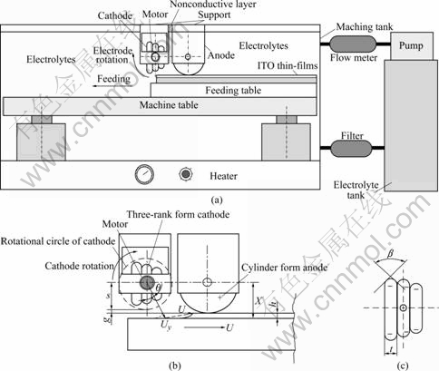
Fig.1 Experimental setup of electroremoving: (a) System schematics; (b) Configuration of tool electrodes (g: Gap width between cathode and workpiece surface; h: ITO thickness (removal depth of electroremoving); s: Radius of rotational circle of cathode); (c) Geometry of negative-electrode (t: Rank thickness of negative-electrode; ��: Arc angle of negative-electrode)
In the current experiment, a design electrode is used and supplied with continuous direct current in the electrochemical machining. The electrolyte is 10% NaNO3 and 5% PO4-3-P (mass fraction). The experimental parameters are electrolyte temperature, current rating, pulsed period, and feed rate of workpiece (displays�� color filter). The amount of the reduction of removal from surface of color filter after electrochemical machining for ITO-film is 150 nm. The flow rate of electrolyte is 5, 10, 15, and 20 L/min. The temperature of the electrolyte is 35, 45, 55, and 65 ��. The current rating is 75, 100, 125, and 150 A. The feed rate of workpiece (displays�� color filter) ranges from 25 to 475 mm/min. The pulsed period (on/off time) uses 100 ms/ 100 ms compared with the continuous direct current. The diameter of the positive-electrode is 30 mm. The rank thickness of the negative-electrode is 3, 6, 9, and 11 mm. The arc angle(��) of the negative-electrode is 30?, 50?, 70? and 90?. All workpieces are put to water cleaning after recycle process then dried by air. The produced ITO-film was measured at more than two locations by a NanoSpec Film Thickness Measurement System (Nanospec Film Analyzer 3000).
3 Results and discussion
3.1 Performance assessment of ITO-film removal
Fig.2 shows that an adequate removal is achieved through a combination of current rating and feed rate of the workpiece (displays�� color filter) for the process of electrochemical machining. At a constant current rating, the workpiece has an optimal feed for the best removal rate. Fast feed reduces the power delivered to a unit area of the workpiece surface, and slow feed increases it. The former could not supply sufficient electrochemical power, while the latter could increase the removal time and the cost. In order to reach the same removal amount of 150 nm for ITO-film, the following combination of parameter values is suggested: 75 A and 300 mm/min, 100 A and 325 mm/min, 125 A and 350 mm/min, 150 A and 375 mm/min. According to the formula of theoretical removal rate on alloy from Faraday Law[11], that is
 (1)
(1)
where �� is the efficiency of current; I is the current; t is time; F is the Faraday constant; ni is the atom number; ai is the proportion of composition; and mi is the atomic mass.
Let ![]() and Uy=
and Uy=![]()
 (2)
(2)
where A is the electrochemical machining area; �� is the density of workpiece; Uy is the removal rate in the longitudinal direction. From the above, the theoretical feed rate of workpiece during the same material removal rate can be calculated. ��, I, F, and A are regarded as constants for the material.
From Fig.1(b), one assumes:
X=s+g+h (3)
where g is the gap width between the electrode (cathode) and surface of ITO (anode); s is the radius of rotational circle of cathode; and h is the removal depth of electroremoving (ITO thickness).
![]() (4)
(4)
(U)sin�� =Uy (5)
Squaring and simplifying Eqs.(4) and (5), one obtains:
![]() (6)
(6)
where U is the feeding velocity of workpiece and Uy is the removal rate in the longitudinal direction. From Eq.(6), one obtains:
 (7)
(7)
From Eq.(7), the experimental results agree well with the theoretical prediction (see Fig.2). Compared with the experimental results, the removal depth x is directly proportional to the current rating I and is the inverse ratio of the feed rate of the workpiece (U), which agrees well with the theoretical prediction (see Fig.2).
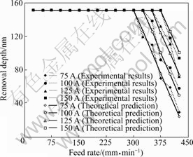
Fig.2 Removal depth at different feed rates of workpiece using different current rating (10% NaNO3 and 5% PO4-3-P, 40 ��, 20 L/min, tool rotation 600 r/min, rank thickness 3 mm, arc angle 90?)
Fig.3 illustrates that the small thickness of the rank reduces the amount of time for effective electroremoval of ITO since the effect of removal is facilitated by supplying sufficient electrochemical power. It also reduces the resistance of dreg discharge and constructs a more effective flushing path along the features of the cathode. Meanwhile, the electrolytic products (dregs) and heat can be removed more rapidly[16, 21]. Importantly, small thickness of the rank provides higher current density, and also has more open space of dregs discharge, improving the removal effect.
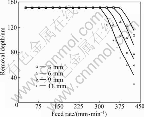
Fig.3 Removal depth at different feed rates of workpiece using different rank thickness of negative-electrode (10% NaNO3 and 5% PO4-3-P, 40 ��, 20 L/min, tool rotation 600 r/min, 150 A, arc angle 90?)
Fig.4 shows the effects of the arc angle of the negative-electrode. Decreasing the arc angle is effective to reduce the resistance of dregs discharge and constructs a more effective flushing path along the surface features of the three-rank form tool. Meanwhile, the electrolytic products and heat can be brought away much rapidly. A small arc angle of the negative-electrode also provides higher current density, which is advantageous for ITO removal. Thus, the smaller the arc angle, the more effective the removal. Fig.5 shows the effects of the pulsed direct current. In order to reach the same removal amount of 150 nm for ITO-film with the continuous direct current, the current rating needs to be increased in proportion to compensate the off-time. One believes that the dregs discharge of electrochemical machining during the off-time is more complete and also has a little bit advantageous to associate with the fast feed rate of workpiece.
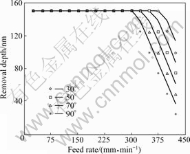
Fig.4 Removal depth at different feed rates of workpiece using different arc angle of negative-electrode (10% NaNO3 and 5% PO4-3-P, 35 ��, 15 L/min, continuous DC 150 A)
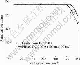
Fig.5 Removal depth at different feed rates of workpiece using continuous and pulsed direct current (10% NaNO3 and 5% PO4-3-P, 40 ��, 20 L/min, tool rotation 600 r/min, rank thickness 3 mm, arc angle 90?)
Fig.6 shows that a higher temperature corresponds to a higher removal rate for ITO-film. One can use the higher temperature to combine with a fast feed rate of color filter to reduce the machining time. Fig.7 shows that the larger the flow rate and the higher the rotational speed of the tool electrodes is, the more rapid the electrolytic depositions, and heat can be brought away, so the removal rate of ITO-film is improved. As a result, the use of large electrolytic flow rate and high rotational speed of the tool electrodes is advantageous to associating with the fast feed rate of workpiece.
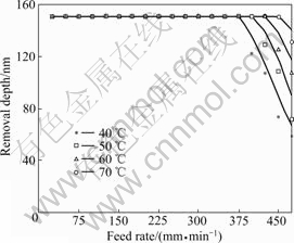
Fig.6 Removal depth at different feed rates of workpiece using different temperature of electrolytes (10% NaNO3 and 5% PO4-3-P, 150 A, 20 L/min, tool rotation 600 r/min, rank thickness 3 mm, arc angle 90?)
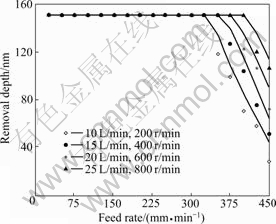
Fig.7 Removal depth at different feed rates of workpiece using different flow rate of electrolytes and different tool rotation (10% NaNO3 and 5% PO4-3-P, 35 ��, 150 A, rank thickness 3 mm, arc angle 90?)
3.2 Specifications requirement of design system
The color filter recovery process is to be extended to all of the in-house CF fabs and adopted into their total recovery systems. The engineering specifications require that defective ITO-film can be removed and the defective color filter can be put back into the production line again. The requirement of technical specifications of the precision recycle-process of ITO-film removal is based on the following considering.
1) Selective removals of ITO-film happen on top of color filter substrates and effectively cut down the production cost.
2) Cost reduction is the ultimate goal when establishing recovery systems based on each fab��s need to recover defective products. The total recovery of the entire system, which prevents re-pollution, is just as important as the function of repairing defective products.
3) Commercialization specifications: (1) It offers recovery process services to major domestic and foreign fabs; (2) It provides an integration of production, equipment, and processing technologies that are based on this research project, namely, direct lead-in of technical services into domestic and foreign fabs and establishment of recovery process lines depending on the needs of in-house CF fabs; (3) Products or technologies derived from implementation of glass recovery systems.
4 Conclusions
A removal process of ITO-film through electrochemical machining is of major interest in current study. The ITO-film can be removed completely by an adequate combination of feed rate of color filter and electric power. Through the ultra-precise removal of thin film microstructure, the defective products in the semiconductor optoelectronic industry can be effectively recycled, reducing production costs. For the removal process, small thickness of the rank provides higher current density, and also has more open space of dregs discharge improving the removal effect. High flow velocity of the electrolyte provides larger discharge mobility and better removal effect. A higher temperature of the electrolyte corresponds to a higher removal rate for ITO-film. An adequate thickness of the negative-electrode, a narrow width of the negative-electrode, or a higher temperature corresponds to a higher removal rate for ITO-film. Higher current rating with a quicker feed rate of color filter effectively reaches the fast promotion of removal effect. Pulsed direct current can improve the effect of dregs discharge and is advantageous to associating with the fast feed rate of workpiece, but raises the current rating.
Acknowledgements
The current study is supported by BEN TEN THE CO., and National Science Council, under contract 96-2622-E-152-001-CC3; 97-2410-H-152-016.
References
[1] IWASE H, MURATA A. Empirical study on improvement of usability for touch-panel for elderly-comparison of usability between touch-panel and mouse [C]// 2002 IEEE International Conference on Systems, Man and Cybernetics. 2002: 252-257.
[2] LAI C C, TSAI C C. Neural calibration and kalman filter position estimation for touch panels [C]// Proceedings of the 2004 IEEE International Conference on Control Applications. 2004: 1491-1496.
[3] TSAI D M, LIN P C, LU C J. An independent component analysis-based filter design for defect detection in low-contrast surface images [J]. Pattern Recognition, 2006, 39(9): 1679-1694.
[4] ZHANG Y, ZHANG J A. Fuzzy neural network approach for quantitative evaluation of Mura in TFT-LCD neural networks and brain [C]// 2005 ICNN&B '05. 2005: 424-427.
[5] DAEIL K, STEVEN K. Effect of secondary ion beam energy and oxygen partial pressure on the structural, morphological and optical properties of ITO films prepared by DMIBD technique [J]. Int J of Surface and Coatings Technology, 2002, 154: 204-208.
[6] KIM H C, KWON B H, CHOI M R. An image interpolator with image improvement for LCD controller [J]. IEEE Transactions on Electronics, 2001, 2: 47-51.
[7] LEE P M, CHEN H Y. Adjustable gamma correction circuit for TFT-LCD [C]// IEEE Conference Proceeding. 2005: 780-783.
[8] WILSON J. Practice and theory of electrochemical machining [M]. New York: Wile-Interscience, 1971: 79-161.
[9] PHILLIPS R E. What is electrochemical grinding and how does it work [J]. Carbide and Tool Journal, 1986, 18: 12-14.
[10] MILEHAM A R, HARREY S J, STOUT K J. The characterization of electrochemically machined surfaces [J]. Wear, 1986, 109: 207-214.
[11] MCGEOUGH J A. Principles of electrochemical machining [M]. London: Chapman and Hall, 1974: 1-10.
[12] BANNARD J. Effect of flow on the dissolution efficiency of mild steel during ECM [J]. Journal of Applied Electrochemistry, 1977, 7: 267-270.
[13] SHEN W M. The study of polishing of electric discharge-machined mold with ECM [D]. Taiwan: National Yunlin Institute of Techndogy, 1995.
[14] MANSOUR S S. Electropolishing of brass alloys in phosphoric acid iskander [J]. Surface Technology, 1980, 10(5): 357-361.
[15] DATTA M, LANDOLT D. Electrochemical machining under pulsed current conditions [J]. Elector Acta, 1981, 26: 899-907.
[16] RAJURKAR, K R. Modeling and monitoring interelectrode gap in pulse electrochemical machining [J]. Annals of the CIRP, 1995, 44: 177-180, 1995.
[17] CAGNON L, KIRCHNER V, KOCK M, SCHUSTER R, ERTL G, GMELIN W T, KUCK H. Electrochemical miromachining of stainless steel by ultra short voltage pulses [J]. Z Phys Chem, 2003, 217: 299-313.
[18] JAIN V K, NANDA V N. Analysis of taper produced in size zone during ECD [J]. Precision Engineering, 1986, 8: 27-33.
[19] HOCHENG H, PA P S. Electropolishing of cylindrical workpiece of tool materials using disc-form electrodes [J]. Journal Materials Processing Technology, 2003, 142: 203-212.
[20] PA P S. Effective form design of electrode in electrochemical smoothing of end turning surface [J]. Journal of Materials Processing Technology, 2008, 195(1/3): 44-52.
[21] KIM B H, RYU S H, CHOI D K, CHU C N. Micro electrochemical milling [J]. Journal of Micromechanics and Microengineering, 2005, 15: 124-129.
Corresponding author: Pai-shan PA; Tel: +886-2-27321104-2214; E-mail:myhow@seed.net.tw
(Edited by YANG Bing)


