
Trans. Nonferrous Met. Soc. China 22(2012) 3003-3011
Structural and optical properties of nano-spin coated sol-gel porous TiO2 films
M. M. El-NAHASS1, M. H. ALI2, A. El-DENGLAWEY3,4
1. Physics Department, Faculty of Education, Ain Shams University, Roxy, Cairo 11757, Egypt;
2. Physics Department, Faculty of Science, Ain Shams University, Cairo, Egypt;
3. Physics Department, Faculty of Science, South Valley University, Qena 83523, Egypt;
4. Phys Dep, Fac of Appl Med Sci Turabah, 21995, Taif University, KSA
Received 15 December 2011; accepted 23 May 2012
Abstract:
Three thicknesses of TiO2 films, 174, 195, and 229 nm, were deposited onto quartz substrates by spin coated sol-gel method. The prepared films were characterized by nano-crystalline structure with different crystallite sizes (19-46 nm) and relatively high porous structure. Optical constants were determined and showed the lowest refractive index of 1.66 for the as-prepared films that ever reported till now. Obtained results were discussed through current theoretical ideas.
Key words:
TiO2 films; optical properties; nanostructure; electron microscopy; thin films; spin coating technique;
1 Introduction
Many theoretical and experimental investigations have been carried out on the electronic transport properties of semi-conducting oxide thin films. Titanium dioxide or titania, TiO2, is a high band gap semiconductor that exhibits high transparency to visible and near infra red (NIR) light. It has three crystalline phases: anatase (tetragonal), rutile (tetragonal), and brookite [1-4]. Both anatase and rutile are more common phases than the brookite and have wide commercial applications.
Rutile is the most thermodynamically stable phase of TiO2. Its refractive index and density are high as compared to anatase phase [5]. Formation of a particular phase depends on the nature of the starting material, its composition, deposition method, and annealing temperatures. TiO2 is a cheap, harmless, white, and non-biodegradable material. Also, it has high refractive index, high dielectric constant, semiconductor properties and chemical stability. It is widely used in various applications such as optical filters [6], gas sensors [7], ceramic membranes [8], wave-guides [9], photo catalysts [11-14] and dye sensitized solar cells [15]. A number of methods have been employed to prepare TiO2 films including electron beam evaporation, sputtering, chemical vapor deposition, laser ablation, polymer technique and sol�Cgel process [16-21]. The sol�Cgel process is a liquid-deposit process using soft chemistry, giving homogeneous deposits. It is less demanding in terms of equipment and is thus less costly, and gives the opportunity to deposit films with large surface areas [22,23].
2 Experimental
TiO2 provided by Millennium inorganic chemicals, SP-300N A Cristal Company, France, was used as the starting material. Three different thicknesses of TiO2 films, 174, 195, and 229 nm, were prepared with a hand made spin coating at 2500 r/min for 30 s. Film thickness (d) was checked by an interferometric method [24]. The specimen of TiO2 films of 70 nm thickness for TEM examination was prepared on a quartz substrate covered by rock salt. TEM specimen was obtained by removing these films from quartz substrate through water immersing and subsequently, these films were picked up on 200-mesh copper grids of 3.05 mm diameter.
The absorption edge and the refractive index of nano TiO2 films were determined by reflectance and transmittance spectra performed on the films deposited on quartz substrates by spin coating technique. The quartz substrate was rinsed with acetone and washed thoroughly with deionized water. The optical measurements were performed by JASCO molel V-570UV-Vis-NIR double beam spectrophotometer in the wavelength range of 200-2500 nm, with a slit width of 3 nm, and a sampling interval of 2 nm. The structure and the optical measurements were performed at room temperature. Structure was analyzed using Philips-CM12 transmission electron microscope (TEM). The reflectance was measured at the normal incidence with an aluminum reference mirror. The absolute values of measured transmittance, T, and reflectance, R, after correcting the absorbance and reflectance of the substrates, are given by [25,26]
 (1)
(1)
where Ift and Iq are the intensities of the light passing through the film-quartz system and the reference quartz, respectively; Rq is the reflectance of quartz. In addition, if the intensity of light reflected from the sample mirror reaching the detector is Ifr and that reflected from the reflectance reference mirror is Im, then
 (2)
(2)
where Im is the intensity of light reflected from the reference mirror, Ifr is the intensity of light reflected from the sample reaching the detector and Rm is the mirror reflectance.
Reflectance and transmittance spectra were performed on thin film samples with single face. Extinction coefficient, k and refractive index, n were calculated using T, R and thickness, d, taking into account the experimental error of the film thickness to be ��2% and of T and R to be ��1%. The error in the calculated values of n and k are estimated to be ��3% and ��2.5%, respectively.
In this work, we have investigated the structure and the optical properties of TiO2 film because of its various friendly applications. Both n and k of TiO2 film were determined from the absolute values of the measured transmittance and reflectance at normal light incidence after correcting the absorbance and reflectance of the substrate as given by Eqs. (1) and (2).
3 Results and discussion
3.1 Structural properties
Structural properties of TiO2 film (70 nm thick) were studied using transmission electron microscope, (TEM). The selected area electron diffraction (SAED) pattern of the as-deposited TiO2 films is shown in Fig.1. The corresponding electron diffraction pattern confirms the polycrystalline nature of TiO2 film. The experimental data show that the TiO2 film has a tetragonal system (rutile system) with lattice constants of a=4.53  , c=2.92 with d=2.153, 2.028, 1.656, 1.461 nm corresponding to Miller indices (111), (210), (211), (002), respectively [27]. The transmission electron microscopy shows nano- crystallites. The size of the observed nano-crystallites was 19-46 nm, as shown in Fig. 2.
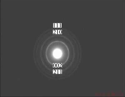
Fig. 1 SAED pattern for TiO2 film
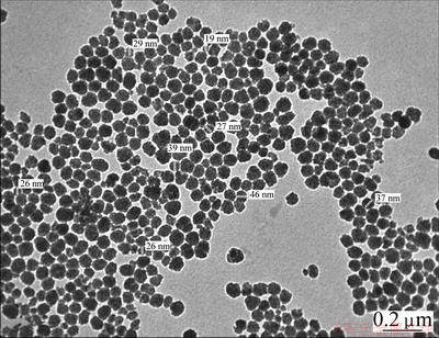
Fig. 2 TEM micrograph for TiO2 film
3.2 Optical properties
3.2.1 Spectral distribution of T and R
The spectral dependences of T and R of the as-prepared TiO2 films of three different thicknesses, 174, 195, and 229 nm, are shown in Fig. 3. The results indicate that T increases with the increasing of the incident photons wavelength, ��, and is independent of the film thickness. One can divide the spectral dependences of both T and R of the as-prepared TiO2 films as a function of �� into two main parts. The first one at ��<1000 nm is called high absorption region, and is characterized by drastic change of both T and R as a function of �� in which T+R<1 where the optical constants were determined. The second one is non absorption region at ��>1000 nm; both T and R are characterized by stability through the whole wavelength range of T+R=1 where refractive index was determined. Figure 3 announces that the percentage of transmission is approximately 95% in the visible and NIR region consequently, the high transmittance inferred that spin coated TiO2 films could be used for optical coating applications. The wavelength of the film absorption edge is 290 nm approximately.
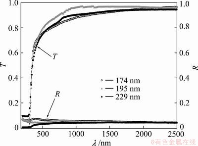
Fig. 3 Dependence of transmission (T) and reflection (R) on wavelength (��) for TiO2 films with thicknesses of 174, 195 and 229 nm
3.2.2 Absorption and extinction coefficient
Both of T, R and thickness, d were used to determine the absorption coefficient, ��, according to [28]
 (3)
(3)
Optical absorption coefficient (��) is given by
 (4)
(4)
The calculated absorption coefficient, ��, versus photon energy, h��, is depicted in Fig. 4. One can observe that �� increases with the increasing of photon energy through the whole range of high absorption region while it decreases through the non-absorbing region. One can observe that both arrow and circle distinguish the end term of Urbach tail region (����104 cm-1) and high absorption region (�� �� 104 cm-1). Extinction coefficient of TiO2 film was calculated by
 (5)
(5)
The calculated values of extinction coefficient, k vs �� for TiO2 films are illustrated in Fig. 5. It could be noticed that k decreases with increasing of ��, and is thickness independent.
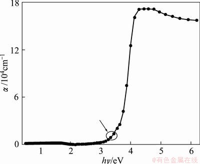
Fig. 4 Absorption coefficient (��) vs photon energy (h��)
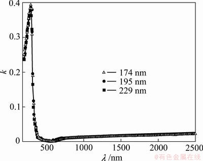
Fig. 5 k vs �� for TiO2 films with thicknesses of 174, 195 and 229 nm
3.2.3 Optical band gap calculation
An absorption edge of semiconductors corresponds to the threshold of charge transition between the highest nearly filled band and the lowest nearly empty band. According to inter-band absorption theory, the optical band the films of can be calculated using the following relation [29]:
 (6)
(6)
where A is the probability parameter for the transition, also the constant A is a measure of the disorder of the material [30], A=4��min/nc��E, where ��min is the minimum metallic conductivity, n is the refractive index, c is the light-velocity, and ��E=��Ec-��Ev represents the band tailing [31];  is the optical band gap of the material, h�� is the incident photon energy; r is the transition coefficient. The reported value of r is 2 for the measurement of indirect band gap and 1/2 for direct band gap. Both direct and indirect band gaps of TiO2 films were found, and the indirect optical band gap is evaluated by extrapolating the straight line part of the curves (��h��)1/2 with energy axes (h��) i.e (��h��)1/2=0 according to
 (7)
(7)
Due to phonon energy assisting the indirect transition [32], Eq. (7) could be written as
 (8)
(8)
where Ephonon is the phonon energy assisting the indirect transition.
Direct optical band gap was evaluated by extrapolating the straight line part of the curves (��h��)2 with energy axes (h��) i.e (��h��)2 =0 according to
 (9)
(9)
Relationship of both  ,
, , and h�� is depicted in Fig. 6. It reveals the simultaneous existence of direct and indirect band gaps in TiO2 films.
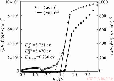
Fig. 6 (��h��)2 and (��h��)1/2 vs Photon energy
Values of direct  , indirect,
  optical band gaps and Ephonon were 3.721, 3.47 and 0.230 eV, respectively. Furthermore, the value of indirect band gap was found to be lower than that of direct band gap. Simultaneous existence of a direct, and indirect, optical band gaps were also reported in Refs. [33-40].
The characters [40-43] augmented our and results. One can observe that both values of and are different by ��E:
��E = -=3.721-3.470=0.251 (eV)
This difference may be attributed to spin orbital splitting [44].
The absorption tail of TiO2 films was analyzed according to [45]
 (10)
(10)
where ��o is a constant and Ec is the band tail width. The absorption coefficient is governed by the so-called ��Urbach rule��.
Figure 7 shows the plot of ln �� versus h�� for TiO2 films. The released straight line indicates that the absorption threshold characterizes an exponential absorption edge.
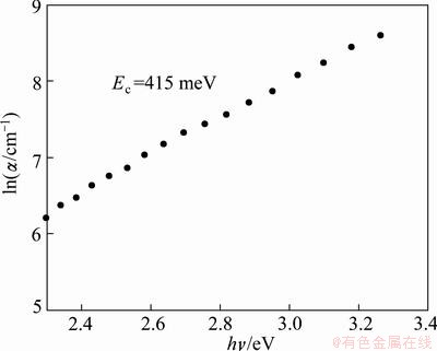
Fig. 7 ln( ��/cm-1) as function of photon energy
The value of Ec for TiO2 films was 415 meV. To the best of our knowledge no such values of Ec and Ephonon in spin coated TiO2 films have not been previously reported.
It is known that rutile is an oxygen-deficit semi-conducting transition metal oxide at room temperature when equilibrated in an atmosphere of low oxygen activity, and is non-conducting at room temperature when equilibrated in an atmosphere of high oxygen activity [46]. Due to the fact that ��the ideal crystal does not exist��, at any temperature crystals contain various structural imperfections or defects. Urbach tail represents the localized states, due to defects in the structure with band tail width of 415 meV. The defect disorder of TiO2 has generally been considered in terms of oxygen vacancies, titanium interstitials and electrons. The oxygen deficiency introduces an excess of electrons included within bandwidth or the tail of the material. These defects are donor-type defects, therefore TiO2 has been considered an n-type semi-conductor [47-50]. So, an indirect transition can be seen as a phonon-assisted electronic transition from the maximum of the valence band to the minimum in the conduction band occurring between different points in k-space. Since the valence and conduction band extrema occur at a different k points in the Brillouin zone, the indirect gap excitation requires a phonon to conserve crystal momentum [51] and other optical constants were available elsewhere [44].
3.2.4 Refractive index and dielectric constant
Both R and k at different �� were used to calculate refractive index, n according to [52]
 (11)
(11)
The spectral dependences of both n(h��) and k(h��) are plotted in Fig. 8. n and k were determined for different film thicknesses. It could be noticed that both n and k are practically independent of film thickness. Therefore, the values used in the plots are the mean values of both n and k. From Fig. 8, one can observe that the tolerance of both n and k lies within the limits of experimental error. The interesting obtained value of n is 1.66 through the wavelength range (300-1200 nm). This is the lowest value reported to the refractive index of the as-prepared spin coated TiO2 films. The porosity of the films is calculated according to [53]
 (12)
(12)
where nd is the refractive index of pore-free anatase (nd= 2.52) [54] and n is the refractive index of the porous thin films (n=1.66). The calculated porosity was found to equal 67.19%. The lowest value of refractive index ever reported till now is 1.05 for SiO2 and is 1.67 for TiO2 [55,56]. The current obtained value of n is so low, it is the lowest value of refractive index ever reported until now for the as- prepared TiO2 films while the lower value of refractive index ever reported until now of annealed TiO2 films is reported elsewhere [57].
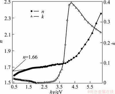
Fig. 8 n and k as function of photon energy
It was reported that the higher refractive indices give an evidence for the fine crystalline of the fabricated films and the correlation between the refractive index and the dielectric constant of a dielectric material. The decrease of the refractive index and packing density can be attributed to the porous structure [16,58]. According to that, the obtained low value of n is attributed to high porous TiO2 films and nano-crystallites. We can say that porous density can be engineered in a continuous range of values to obtain low refractive index material. The dispersion of refractive index of TiO2 films was analyzed using the concept of the single oscillator and could be expressed by the Wemple�CDiDomenico (WDD) relationship [59] as
 (13)
(13)
where h�� is the photon energy, Eo is the single-oscillator energy and Ed is the dispersion energy which is a measure of the intensity of the inter-band optical transition, and does not depend significantly on the band gap. Plotting  vs (h��)2 shown in Fig. 9 allows to determine the oscillator parameters by fitting a straight line to the experimental points according to Ref. [60]. The obtained values of the single oscillator energy Eo and the dispersion energy Ed were 4.59 and 7.3 eV respectively. By extrapolating the linear part of WDD, optical dispersion relationship towards the infrared spectral region (h��=0), static refractive index n(0), could be defined by the infinite wavelength dielectric constant ����, which can be deduced to be 2.637. The relationship between the lattice dielectric constant ��L, and the refractive index, n is given by [61]
 (14)
(14)
where ��L is the lattice dielectric constant; N/m* is the ratio of the carrier concentration to the effective mass; c is the speed of light; e is the electronic charge; ��o is the permittivity of free space.
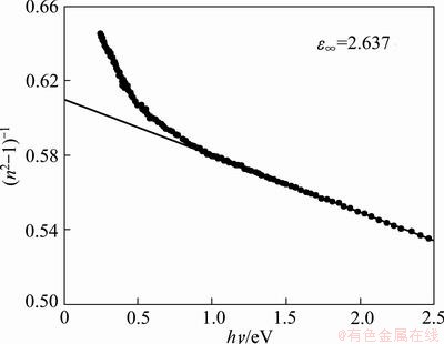
Fig. 9 (n2-1)-1 vs (h��)2 for TiO2 film
The plots of n2 versus ��2, are shown in Fig. 10, which is linear verifying of Eq. (14). The value of ��L is determined from the extrapolation of these plots to ��2 =0 and N/m* from the slope of the graph. The obtained results are ��L=2.769 and N/m* =9.5�� 1037 kg-1��m-3. The disagreement between the values of ���� and ��L may be due to the free carrier concentration [62,63]. The obtained values of n and k were used to calculate both real, ��1 and imaginary part, ��2 of dielectric constant, ��:
��=��1-j��2, ��1=n2-k2 and ��2=2nk (15)
where ��1 determines the maximum energy that can be stored in the material; ��2, also is called the relative loss factor, represents the absorption of electrical energy by a dielectric material that is subjected to an alternating electromagnetic field. The loss tangent tan ��, tan��=��1/��2, determines how well a material can absorb the electromagnetic field [64], where the angle �� is the phase difference between the applied electric field and the induced current [63]. Figures 11 and 12 show the variation of both ��1, ��2 and tan�� as a function of photon energy. After 2 eV energy value, both ��1, ��2 and tan�� increase forward as the photon energy increases except ��2 and tan�� display a maximum starting around 3.7 eV which corresponds to direct energy gap.
3.2.5 Optical conductivity
The optical conductivity is one of the powerful tools for studying the electronic states in materials [65,66]. If a system is subjected to an external electric field, in general, a redistribution of charges occurs and currents are induced. For small enough fields, the induced polarization and the induced currents are proportional to the inducing field.
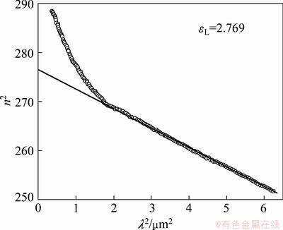
Fig. 10 Plot of n2 vs ��2
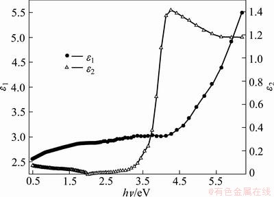
Fig. 11 ��1 and ��2 as function of photon energy
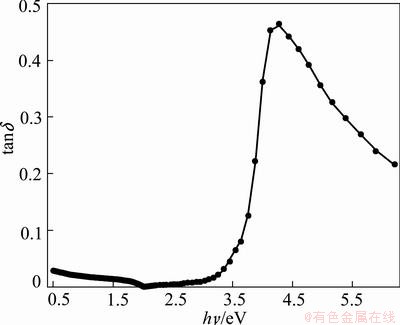
Fig. 12 tan �� vs photon energy
The complex optical conductivity, �� is related to the complex dielectric constant, �� by [67]
 (16)
(16)
where �� is the angular frequency; ��0 is the free space dielectric constant.
The real, ��1 and imaginary, ��2 parts of the optical conductivity dependence of energy are shown in Fig. 13.
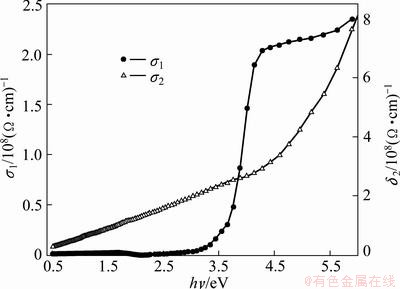
Fig. 13 ��1 and ��2 as function of photon energy
It is seen that the optical conductivity increases with increasing photon energy, which has drastically increasing corresponding to the absorption edge and the optical gap. This suggests that the increase in optical conductivity is due to electrons excited by photon energy. The origin of this increasing may be attributed to some changes in the structure due to the charge ordering effect [68].
4 Conclusions
The deposition of TiO2 was performed on quartz substrates at room temperature in air for three different thicknesses. Structural studies confirm that TiO2 films have tetragonal system or rutile phase characterized by nanocrystallite size. Optical constants like optical energy gap (direct and indirect) and Urbach tail had been determined to be 3.721 eV, 3.47 eV, and 415 meV, respectively. Indirect optical gap was phonon assisted with energy of 0.230 eV. The difference, ��E, between values of direct and indirect optical band gap was 0.251 eV and attributes to spin orbital splitting. Low-refractive- index of the as-prepared TiO2 with the unprecedented refractive index of 1.66 is demonstrated. This low value was attributed to high ratio of porosity (67.19 %) and nano-structure. The obtained values of the oscillator energy, Eo and oscillator strength, Ed are 7.3 and 4.59 eV, respectively.
The values of the dielectric constant ����, lattice dielectric constant ��L, and the ratio of the carrier concentration to the effective mass and N/m* are 2.637, 2.769, and N/m*=9.5��1037 kg-1��m-3, respectively. The disagreement between the values of ���� and ��L was attributed to the free carrier concentration. The real part of the dielectric constant is higher than the imaginary part through non-absorbing region. The loss tangent, tan �� appears to show a drastic increasing at photon energy range of 3.5-4 eV that corresponds to optical energy gap range and absorption energy due to interband transition. Optical conductivity was found to increase as a function of photon energy.
References
[1] WANG Z, HELMERSSON U, KALL P. Optical properties of anatase TiO2 thin films prepared by aqueous sol-gel process at low temperature [J]. Thin Solid Films, 2002, 405: 50-45.
[2] SHCHUKIN D G, SVIRIDOV D V, PHOTOCHEM J, PHOTOBIOL C. Photocatalytic processes in spatially confined micro- and nan-reactors photochem [J]. J Photochem Photobiol C: Photochemistry Reviews, 2006, 7: 23-39.
[3] ZHANG R, GAO L, ZHANG Q. Photodegradation of surfactants on the nanosized TiO2 prepared by hydrolysis of the alkoxide titanium [J]. Chemosphere, 2004, 54: 405-411.
[4] RICHARDON S, THRUSTON A, COLLETTE T, PATTERSON K, LYKINS B. Identification of TiO2/UV disinfection byproducts in drinking water [J]. Environ Sci Technol, 1996, 30: 3327-3334.
[5] BACH H, KRAUSE D. Thin films on glass [M]. Heidelberg: Springer, 1997.
[6] KOSTLIN H, FRANK G, HEBBINGHAUS G, AUDING H, DENISSEN K. Optical filters on linear halogen-lamps prepared by dip-coating [J]. J Non-Cryst Solids, 1997, 218: 347-353.
[7] TANG H, PRASAD K, SANJINES R, LEVY F. TiO2 anatase thin films as gas sensors [J]. Sens Actuat B, 1995, 26-27: 71-75.
[8] YAN Y, CHAUDHURI S R, SARKAR A. Synthesis, characterizations, and optical properties of stacked porous thin films derived from sol�Cgel process [J]. J Am Ceram Soc, 1996, 79: 1061-1065.
[9] ZHAI J, YANG T, ZHANG L, YAO X. The optical wave guiding properties of TiO2-SiO2 composite films prepared by the sol-gel process [J]. Ceram Int, 1999, 25: 667-670.
[10] YU J, ZHAO X, ZHAO Q. Photocatalytic activity of nanometer TiO2 thin films prepared by the sol�Cgel method [J]. Mater Chem Phys, 2001, 69: 25-29.
[11] LINSEBIGLER A L, LU G, YATES J T Jr. Photocatalysis on TiO2 surfaces: Principles, mechanisms, and selected results [J]. Chem Rev, 1995, 95: 735-758.
[12] MILLS A, le HUNTE S. An overview of semiconductor photocatalysis [J]. J Photochemistry and Photobiology A, 1997, 108: 1-35.
[13] LEGRINI O, OLIVEROS E, BRAUN A M. Photochemical processes for water treatment [J]. Chem Rev, 1993, 93: 671-698.
[14] HOFFMANN M R, MARTIN S T, CHOI W, BAHNEMANN D W. Environmental applications of semiconductor photocatalysis [J]. Chem Rev, 1995, 95: 69-96.
[15] KO K H, LEE Y C, JUNG Y J. Enhanced efficiency of dye-sensitized TiO2 solar cells (DSSC) by doping of metal ions [J]. J Colloid Interf, 2005, 283: 482-487.
[16] WANG S, XIA G, HE H, YI K, SHAO J. Structural and optical properties of nanostructured TiO2 thin films fabricated by glancing angle deposition [J]. J Alloys and Compounds, 2007, 431: 287-291.
[17] TAKEDA S, SUZUKI S, ODAKA H, HOSONO H. Photocatalytic TiO2 thin film deposited onto glass by DC magnetron sputtering [J]. Thin Solid Films, 2001, 392: 338-344.
[18] HA H Y, NAM S W, LIM T H, OH I H, HONG S A. Properties of the TiO2 membranes prepared by CVD of titanium tetraisopropoxide [J]. J Membr Sci, 1996, 111: 81-92.
[19] LIU Pei-sheng, CAI Wei-ping, WAN Li-xi, SHI Ming-da, LUO Xiang-dong, JING Wei-ping. Fabrication and characteristics of rutile TiO2 nano particles induced by laser ablation [J]. Transactions of Nonferrous Metals Society of China, 2009, 19: s743-s747.
[20] KARTHICK S N, PRABAKAR K, SUBRAMANIA A, JANG J J, KIM HCE-JE. Formation of anatase TiO2 nanoparticles by simple polymer gel technique and their properties [J]. Powder Technol, 2011, 205: 36-41.
[21] BOUABID K, IHLAL A, AMIR Y, SDAQ A, ASSABBANE A, AIT-ICHOU Y, OUTZOURHIT A, AMEZIANE E L, NOUET G. Optical study of TiO2 thin films prepared by sol-gel [J]. Ferroelectrics, 2008, 372: 69-75.
[22] BRINKER C J, SCHERER G W. Sol�Cgel science [M]. San Diego, CA: Academic Press, 1990.
[23] RATH C, MOHANTY P, PANDEY V, MISHRA N C. Oxygen vacancy induced structural phase transformation in TiO2 nanoparticles [J]. J Phys D, 2009, 42: 205101.
[24] TOLANSKY S. Multiple beam interferometry of surfaces and films [M]. London: Oxford University Press, 1988: 147.
[25] BAKRY A M, EL-NAGGAR A H. Doping effects on the optical properties of evaporated Si:H films [J]. Thin Solid Films, 2000, 360: 293-297.
[26] El-NAGGAR A H. Optical properties of Al-doped a-Si:H films [J]. J Phys C: Condensed Matter, 1999, 11: 9619-1928.
[27] International Centre for Diffraction Data, JCDS 88��1174.
[28] EL MANDOUH Z S, SELIM M S. Physical properties of vanadium pentoxide sol gel films [J]. Thin Solid Films, 2002, 371: 259-263.
[29] KIREEV P. La physics of semiconductors [M]. Mir ed. Moscou, 1975.
[30] TAUC J. Amorphous and liquid semiconductors [M]. New York: Plenum, 1976.
[31] EL-DENGLAWEY A, DONGOL M, EL-NAHASS M M. Photoinduced absorption edge shift of As20Se60Tl20 films [J]. J Lumin, 2010, 130: 801-804.
[32] PANKOVE J I. Optical processes on semiconductors [M]. New Jersey: Prentice-Hall, 1971.
[33] MATHAI C J, SARAVANAN S, ANANTHARAMAN M R, VENKITACHALAM S, JAYALEKSHMI S. Effect of iodine doping on the bandgap of plasma polymerized aniline thin films [J]. J Phys, D, 2002, 35: 2206-2210.
[34] SHAH JALAL A B M, AHMED S, BHUIYAN A H, IBRAHIM M. UV-vis absorption spectroscopic studies of plasma-polymerized m-xylene thin films [J]. Thin Solid Films, 1996, 288: 108-111.
[35] SHARMA T, AGRWAL S, KUMAR S, MITTAL V K, KALSI P C, MANCHANDA V K. Effect of gamma irradiation on the optical properties of CR-39 polymer [J]. J Mater Sci, 2007, 42: 1127-1130.
[36] HIRANKUMAR G, SELVASEKARAPANDIAN S, KUWATA N, KAWAMURA J, HATTORI T. Thermal, electrical and optical studies on the poly(vinyl alcohol) based polymer electrolytes [J]. J Power Sources, 2005, 144: 262-267.
[37] YASAKI Y, SONOYAMA N, SAKATA T. Semiconductor sensitization of colloidal In2S3 on wide gap semiconductors [J]. J Electroanal Chem, 1999, 469: 116-122.
[38] JIN M S, KIM N O, KIM G, YOON C S, LEE I C, KIM M Y, KIM W T. Optical properties of undoped and Co2+ -doped CaS, CaSe, BaS, and base single crystals [J]. J Korean Phys Soc, 2001, 39: 692-697.
[39] HASAN M M, HASEEB A S M A, SAIDUR R, MASJUKI H H, HAMDI M. Influence of substrate and annealing temperature on optical properties of RF-sputtered TiO [J]. Optical Materials, 2010, 32: 690-695.
[40] JANITABAR-DARZI S, MAHJOUB A R, NILCHI A. Investigation of structural, optical and photocatalytic properties of mesoporous TiO2 thin film synthesized by sol-gel templating technique [J]. Physica E, 2009, 42: 176-181.
[41] ELFANAOUI A, ELHAMRI E, BOULKADDAT L, IHLAL A, BOUABID K, LAANAB L, TALEB A, Portier X. Optical and structural properties of TiO2 thin films prepared by sol-gel spin coating [J]. Int J hydrogen Energy, 2011, 36: 4130-4133.
[42] TERESA M, VISEU R, ISABEL M, FERREIRA C. Morphological characterization of TiO2 thin films [J]. Vacuum, 1999, 52: 115-120.
[43] PARK Y R, KIM K J. Structural and optical properties of rutile and anatase TiO2 thin films: Effects of co doping [J]. Thin Solid Films, 2005, 484: 34-38.
[44] WAKAKI M, KUDO K, SHIBUYA T. Physical properties and data of optical materials [M]. New York: CRC Press, 2007.
[45] URBACH F. The long-wavelength edge of photographic sensitivity and of the electronic absorption of solids [J]. Phys Rev, 1953, 92: 1324-1324.
[46] BALACHANDRAN U, N G EROR. Electrical conductivity in non-stoichiometric titanium dioxide at elevated temperatures [J]. J Mat Sci, 1988, 23: 2676-2682.
[47] MATZKE H J. Diffusion in non-stoichiometric oxides [C]// Nonstoichiometric Oxides. SORENSEN O T. New York: Academic Press, 1981.
[48] KOFSTAD P. Nonstoichiometry, diffusion, and electrical conductivity in binary metal oxides [M]. New York: Wiley-Interscience, 1972.
[49] NOWOTNY J, BAK T, SORRELL C C, SHEPPARD L R. Materials and devices for energy conversion [M]. Cambridge: Woodhead, 2005: 84-116.
[50] NOWOTNY M K, BAK T, NOWOTNY J. Electrical properties and defect chemistry of TiO2 single crystal electrical conductivity [J]. J Phys Chem B, 2006, 110: 16270-16282.
[51] DRESSELHAUS M S. Solid state physics: Part 2��Optical properties of solids. [2012-05-05]. URL: http://web.mit.edu/course/ 6/6.732/ OldFiles/www/ 6.732-pt2.pdf.
[52] MOSS T S. Optical process in semiconductor [M]. London: Butter Worths, 1959.
[53] YOLDAS B E, PARTLOW P W. Formation of broad band antireflective coatings on fused silica for high power laser applications [J]. Thin Solid Films, 1985, 129: 1-14.
[54] KINGERY W D, BOWEN H K, UHLMANN D R. Introduction to ceramics [M]. New York: Wiley, 1976.
[55] XI J Q, SCHUBERT M F, KIM J K, SCHUBERT E F, CHEN M, YULIN S, LIU W, SMART J A. Optical thin-film materials with low refractive index for broadband elimination of Fresnel reflection [J]. Nature Photonics, 2007, 1: 176-179.
[56] SCHUBERT E F, KIM J K, XI J Q. Low-refractive-index materials: A new class of optical thin-film materials [J]. Phys Stat Sol B, 2007, 244: 3002-3008.
[57] NACEUR J B, GAIDI M, BOUSBIH F, MECHIAKH R, CHTOUROU R. Annealing effects on microstructural and optical properties of nanostructured-TiO2 thin flms prepared by sol-gel technique [J]. Curr Appl Phys, 2012, 12: 422-428.
[58] TANEMURAA S, MIAO L, JIN P, KANEKO K, TERAI A, NABATOVA-GABAIN N. Optical properties of polycrystalline and epitaxial anatase and rutile TiO2 thin films by rf magnetron sputtering [J]. Appl Surf Sci, 2003, 212-213: 654-660.
[59] WEMPLE S H, DIDOMENICO M. Behavior of the electronic dielectric constant in covalent and ionic materials [J]. Phys Rev B, 1971, 3: 1338-1351.
[60] EL-DENGLAWEY A. Characterization of As-Se-Tl films near infrared region J [J]. Non-cryst Solids, 2011, 357: 1757-1763.
[61] KUMAR G A, THOMAS J, GEORGE N, KUMAR B A, SHNAN P R, NPOORI V P, VALLABHAN C P G, UNNIKRISHNAN N V. Optical absorption studies of free (H2Pc) and rare earth (RePc) phthalocyanine doped borate glasses [J]. Phys Chem Glasses, 2001, 41: 89-93.
[62] EL-NAHASS M M, DONGOL M, ABOU-ZIED M, EL-DENGLAWEY A. The compositional dependence of the structural and optical properties of amorphous As20Se80-xTlx films [J]. Physica B, 2005, 368: 179-187.
[63] EL-NAHASS M M, FARAG A A M, IBRAHIM E M, ABD-EL-RAHMAN S. Structural, optical and electrical properties of thermally evaporated Ag2S thin films [J].Vacuum, 2004, 72: 453-460.
[64] NGUYEN V Q, SANGHERA J S, LLOYD I K, AGGARWAL I D, GERSHON D. Room temperature dielectric properties of the As40S(60-x)Sex glass system [J]. J Non-cryst Solids, 2000, 276: 151-158.
[65] LOSURDO M, GIANGREGORIO M M, LUCHENA M, CAPEZZUTO P, BRUNO G, TORO R G, MALANDRINO G, FRAGALA I L, LO NIGRO R. Structural�Coptical study of high- dielectric-constant oxide films [J]. Appl Surf Sci, 2006, 253: 322-327.
[66] TOHYAMA T, MAEKAWA S. Effects of carrier-doping on optical conductivitya in high Tc copper oxides [J]. J Phys Soc Jpn, 1991, 60: 53-56.
[67] WIKTOREZYK T. Preparation and optical properties of holmium oxide thin films [J]. Thin Solid Films, 2002, 405: 238-242.
[68] KIMURA S, OKUNO M, IWATA H, NISHI T, AOKI H, OCHIAI A. Low-energy optical conductivity of Yb4As3 [J]. Physica B, 2002, 312-313: 356-358.
�ܽ�-������תͿ�����Ʊ��Ķ������������Ĥ�Ľṹ��ѧ����
M.M. El-NAHASS1, M. H. ALI2, A. El-DENGLAWEY3,4
1. Physics Department, Faculty of Education, Ain Shams University, Roxy, Cairo 11757, Egypt;
2. Physics Department, Faculty of Science, Ain Shams University, Cairo, Egypt;
3. Physics Department, Faculty of Science, South Valley University, Qena 83523, Egypt;
4. Phys Dept Fac of Appl Med Sci Turabah, 21995, Taif University, KSA
ժ Ҫ�������ܽ�-������תͿ��������ʯӢ�����ϳ������ֲ�ͬ��ȵ�TiO2��Ĥ�����ȷֱ�Ϊ174��195��229 nm�������õ��ı�Ĥ���ɳߴ�Ϊ19~46 nm ����������ɵģ������нϸߵĶ�ṹ���ⶨ�˱�Ĥ�Ĺ�ѧ�������õ�������Ϊֹ���������������1.66���������ý�����������ۡ�
�ؼ��ʣ�TiO2��Ĥ����ѧ���ܣ����ṹ��������������Ĥ����תͿ������
(Edited by YANG Hua)
Corresponding author: A. El-DENGLAWEY; Tel: +201091922044, +20965216663(Home); E-mail: denglawey@lycos.com
DOI: 10.1016/S1003-6326(11)61563-X
Abstract: Three thicknesses of TiO2 films, 174, 195, and 229 nm, were deposited onto quartz substrates by spin coated sol-gel method. The prepared films were characterized by nano-crystalline structure with different crystallite sizes (19-46 nm) and relatively high porous structure. Optical constants were determined and showed the lowest refractive index of 1.66 for the as-prepared films that ever reported till now. Obtained results were discussed through current theoretical ideas.
[5] BACH H, KRAUSE D. Thin films on glass [M]. Heidelberg: Springer, 1997.
[22] BRINKER C J, SCHERER G W. Sol�Cgel science [M]. San Diego, CA: Academic Press, 1990.
[27] International Centre for Diffraction Data, JCDS 88��1174.
[29] KIREEV P. La physics of semiconductors [M]. Mir ed. Moscou, 1975.
[30] TAUC J. Amorphous and liquid semiconductors [M]. New York: Plenum, 1976.
[32] PANKOVE J I. Optical processes on semiconductors [M]. New Jersey: Prentice-Hall, 1971.
[52] MOSS T S. Optical process in semiconductor [M]. London: Butter Worths, 1959.
[54] KINGERY W D, BOWEN H K, UHLMANN D R. Introduction to ceramics [M]. New York: Wiley, 1976.
