
���±��: 1004-0609(2006)03-0495-05
Sn-3.5Ag-0.5Cu/Cu��������ṹ
�� ��, �Ƽ̻�, �Ž���, ������
(�����Ƽ���ѧ ���Ͽ�ѧ�빤��ѧԺ, ���� 100083)
ժ Ҫ��
�о�����-����ѭ��������Sn-3.5Ag-0.5Cuǥ��/Cu��������ṹ, �����˽�������仯�����������Ϊ, �������ʱЧ���Sn-3.5Ag-0.5Cu/Cu��������˶Աȡ� �������: ����ʱЧ��100h, Sn-3.5Ag-0.5Cu/Cu���������γ�Cu6Sn5��Cu3Sn��������仯����; ����-����ѭ����720��Sn-3.5Ag-0.5Cu/Cu������ֻ����Cu6Sn5�����仯�����, ��Cu3Sn������, �ڽ�������ǥ����, ����״��Ag3Sn�ۼ�����ɿ�״; ����-����ѭ���ͺ���ʱЧ������, ��������仯�������̬��ʼ��Ϊ�ȱ�״, ����ʱЧʱ����ӳ�������ƽ��, �����Բ�״��ʽ������
�ؼ���: ��-����ѭ��; ����ʱЧ; Sn-3.5Ag-0.5Cu/Cu����; �����仯���� ��ͼ�����: TG42
���ױ�ʶ��: A
Microstructure of Sn-3.5Ag-0.5Cu/Cu interface
WANG Ye, HUANG Ji-hua, ZHANG Jian-gang, QI Li-hua
(School of Materials Science and Engineering,
University of Science and Technology Beijing, Beijing 100083, China)
Abstract: The microstructure of Sn-3.5Ag-0.5Cu /Cu interface after thermal-shearing cycling was investigated. Compared with Sn-3.5Ag-0.5Cu /Cu interface after isothermal aging, the development of interfacial IMC during thermal-shearing cycling was studied too. The results show that Cu6Sn5 and Cu3Sn IMC layers have formed at the interface of Sn-3.5Ag-0.5Cu/Cu after isothermal aging for 100h, while only Cu6Sn5 IMC layer, no Cu3Sn layer, presents at the Sn-3.5Ag-0.5Cu/Cu interface after thermal-shearing cycling for 720 cycles, and particle-like phase Ag3Sn grows into massive phase in the field near to the interface. The interfacial IMC exists as scallop-like in the initial aging, during either thermal-shearing cycling or isothermal aging. Then they gradually grow up to planar-like with the aging time increasing.
Key words: thermal-shearing cycling; isothermal aging; Sn-3.5Ag-0.5Cu/Cu interface; intermetallic compound (IMC)
�ڵ�����װ��Ӧ����㷺����Sn-Pbǥ��, ��Pb��һ���ж�Ԫ��, �����뺬Ǧ���ʽӴ��������彡�����Σ��, ȫ���緶Χ�ڽ�ֹPb��ʹ�����Ǵ�������[1-7]�� ���ѿ����о����ڶ���Ǧǥ����, Sn-Ag-Cuϵ�Ͻ����ھ�����������ʪ���ܺ���ѧ����, �ѱ��ձ���Ϊ������DZ����Sb-Pbǥ�ϵ����Ʒ[8-10]�� ������װ����õ�ӡ�Ƶ�·������������������ΪCu�� ���, �о�ǥ�ϺϽ���Cu����Ľ��淴Ӧ���ں���ɿ���Ԥ�⡢ �߿ɿ�����ǥ�����������ǵ�ǰ��������Ǧǥ�ϵĿ�����������Ҫ���塣
Ŀǰ�������Sn-Ag-Cu��Ǧǥ��/Cu����Ľ��淴Ӧ���кܶ��о�[10-15]�� ���е��о����������������еĽ��淴Ӧ�Ƚϳ��; ���ں�����۹����еĽ��淴Ӧ, ���е��о���Ҫ�����ں���ʱЧ����ѭ����������ЧӦ�Ժ�����淴Ӧ��Ӱ�췽�档 ʵ����, �����ڳ�����ѭ���¶��غ�ʱ, ����ӡˢ��·�塢 ����ǥ�ϡ� ������װԪ������������ϵ�����ںܴ����, �����ڲ�������Ӧ��Ӧ��ѭ��(��Ҳ�Ǻ�������ѭ��������ʧЧ�ĸ���ԭ��)�� ����, ������װSn����ǥ�ϺϽ��۵���ٽᾧ�¶ȶ��ܵ�, Ӧ����ζԺ�������������ڲ������ʴ��䡢 ��������κ˺�������������Ӱ�졣 ���, �����к��������Ϊ�����ʱЧ����ѭ�������º��������Ϊ���ű������� ���������о�����-����ѭ��(����ͬʱ������ѭ���غɺͼ���ѭ���غ�)������Sn-3.5Ag-0.5Cu/Cu����Ľ������ṹ�� Ӧ��ɨ��羵�����������ֶ�, �о��˽��漰���������仯���P��������Ϊ, �������ʱЧ��ĺ����������˶Աȡ�
1 ʵ��
ʵ�����ģ������, ��ͼ1��ʾ�� ������ͭ��������������ǥ�����ɡ� �����ٺ�ͭ��������ϵ�����ϴ�(��Ϊ4.6��10-6 ��-1, ͭΪ16.5��10-6 ��-1), ����ѭ����������������ǥ����ͷ��ͬ����������Ӧ��Ӧ��ѭ���� ǥ��ѡ�ñ��㷺�Ͽɵ�Sn-3.5Ag- 0.5Cu�Ͻ� ��������Ϊ100mm, ͭ������Ϊ110mm�� �ٵ���ǥ���ԱȽϲ�, Ϊ��ֹǥ��/Cu����ʧЧǰ�����������λ����ʧЧ, ǥ��ǰ����ɢ����������������ǥ����λ����Ni��(���Ϊ0.1mm)�� ǥ��ʱ, ��ͭ��������֮����ú��Ϊ0.2mm�Ľ�����Ƭ�Կ��ƺ����϶�� �����������ڼ���ƽ̨�Ͻ���ǥ��, ǥ����ֵ�¶�Ϊ230�档 ʵ�����ò��Ͼ������ñ�ͪ�;ƾ���ϴ��
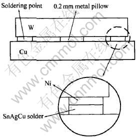
ͼ1 ģ������ʾ��ͼ
Fig.1 Sketch map of simulation samples
��ǥ��������������-����ѭ��ʵ�顣 ��-����ѭ���¶ȷ�ΧΪ25~125�档 ��-����ѭ������Ϊ1h, ������������202�͵��Ⱥ��º����, ��125�汣��30min, ȡ��������25�����30min�� �������ֱ����24�� 200�� 400�� 720����ѭ���� Ϊ�Աȷ���, ���к���ʱЧʵ�顣 ��������125��ֱ���12�� 100�� 360�� 720h�� �����и��ĺ����������Ʋ����, ��5%HClˮ��Һ����ʴ�� Ӧ��LEO-1450�͵���ɨ��羵�۲������������ṹ, ����KEVEX sigma����ϵͳ�Խ�����֯������������
2 ���������
2.1 ʱЧǰSn-3.5Ag-0.5Cu/Cu��������ṹ
ͼ2��ʾΪʱЧǰSn-3.5Ag-0.5Cu/Cu�����ɨ��羵��Ƭ�� ͼ�д��ϵ�������Ϊǥ�ϡ� ��������仯������Cu���塣 δ��ʱЧ�ĺ�����Sn-3.5Ag-0.5Cu/Cu���洦�γ���һ���ȱ�״�Ľ����仯�����, ���������(����1)˵���˻�����ΪCu6Sn5�� �����ȱ�״��̬�����ڸ����ʷ�Ӧ�ķ���, �����ڻ�����ʱ, ����ǥ����Cu���巴Ӧ, �����ȱ�״Cu6Sn5��[3]��
2.2 ����ʱЧ��Sn-3.5Ag-0.5Cu/Cu��������ṹ
ͼ3��ʾΪ125��ʱЧ��ͬʱ���Sn-3.5Ag-0.5Cu/Cu�����ɨ��羵��Ƭ�� ���Կ���, ʱЧ��Ľ�������仯������Ϊ����, ���������(����1)�����ֱ�ΪCu6Sn5���Cu3Sn�㡣 ʱЧ100h���SEM��Ƭ��ʾ(ͼ3(a)), ��Cu6Sn5���Cu�����������һ��ܱ���Cu3Sn, ������ϸ�۲�ſ��Է��֡� ʱЧ360h��720h��, Cu3Sn�ĺ����������(ͼ3(b)��(c))�� ����ʱЧʱ����ӳ�, �����仯�������ܺ��Ҳ������, ����̬���ȱ�״���״ת�䡣 ��Cu-Sn��Ԫ��ͼ��֪, �ڳ�����Cu��Sn�����γ�Cu6Sn5��Cu3Sn�����ȶ��Ļ���� ����Cu3Sn��Cu��Sn��Ħ���ȸߴ�3��1, ����ֻ����Snԭ�ӹ�������������Cu3Sn�Ż����ɡ� ʵ�����õ�Sn-3.5Ag-0.5Cuǥ����, Sn�����ܸ�, Ϊ96%�� �����ǥ��ʱ, �����е�Cu��ǥ���е�Sn��Ӧ�������������ܵ�Cu6Sn5�����仯����㡣 ������ʱЧ������, �����е�Cuԭ�Ӻ��Ѵ���Cu6Sn5����ɢ��ǥ��һ��, ֻ����Cu6Sn5������Ӧ����Cu3Sn�� �˽���ͺܶ�������ı�����һ�µ�[10, 12-14]��
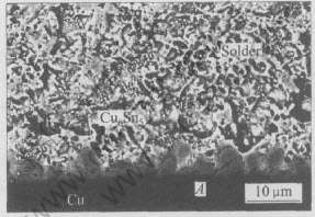
ͼ2 ʱЧǰSn-3.5Ag-0.5Cu/Cu�����ɨ��羵��Ƭ
Fig.2 SEM image of Sn-3.5Ag-0.5Cu/Cu interface before aging
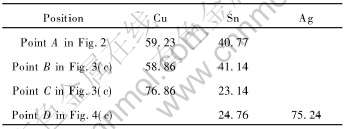
��1 SnAgCu/Cu���漰�����IMC�����������
Table 1 EDX analysis of IMC at SnAgCu/Cu
interface and its neighborhood (mole fraction, %)
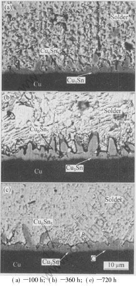
ͼ3 125�����ʱЧ��Sn-3.5Ag-0.5Cu/Cu�����ɨ��羵��Ƭ
Fig.3 SEM images of Sn-3.5Ag-0.5Cu/Cu interface after isothermal aging at 125��
2.3 ��-����ѭ����Sn-3.5Ag-0.5Cu/Cu��������ṹ
��-����ѭ�����Sn-3.5Ag-0.5Cu/Cu����ɨ��羵��Ƭ��ͼ4��ʾ�� ���Կ���, ��-����ѭ������Sn-3.5Ag-0.5Cu/Cu����ֻ���ڵ�һ����Cu6Sn5��, ���»��������֡� ��ʱ����-����ѭ��ʱЧʱ, Cu6Sn5���Ա����ȱ�״(��ͼ4(a))�� ������-����ѭ��ʱЧʱ����ӳ�, �ȱ�״��̬������ƽ��, ����Բ�״��̬����(��ͼ4(b)��(c))�� ��-����ѭ����720��(125���ۼ�ͣ��ʱ��360h), ��������仯������Ȼֻ��Cu6Sn5, û������Cu3Sn�� ���ں���ʱЧ100hʱ, ������������һ��ܱ���Cu3Sn��, 360h���SEM��Ƭ�� Cu3Sn���ѷdz������� ��-����ѭ����720��û������Cu3Sn, ������������������Cuԭ�Ӵ���Cu6Sn5�����仯�������ɢ��ǥ��һ��, ��Sn��Ӧ����Cu6Sn5�� Ҳ����˵, Cu6Sn5��û����Ч�赲Cuԭ�ӵ���ɢ�� ��Ϊԭ�ӵ���ɢ��Ҫ��ͨ�����硢 λ���� ��λ��ȱ����ʵ�ֵ�, ���Ժ�������-����ѭ��������, ����ͭ���ٵ�������ϵ������, �����ڲ���������Ӧ��-Ӧ��ѭ��, ���½�����Cu6Sn5�����仯�������ڹ���ȱ��, ΪCuԭ�ӵ���ɢ�ṩ��ͨ���� Cu6Sn5�����仯�������и�Ӳ�Ⱥߴ���, ���׳�Ϊ������ѵ�����Դ, ����ʧЧ��
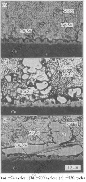
ͼ4 ��-����ѭ��ʱЧ��Sn-3.5Ag-0.5Cu/Cu�����ɨ��羵��Ƭ
Fig.4 SEM images of Sn-3.5Ag-0.5Cu/Cu
interface after thermal-shearing cycling aging
����Sn-3.5Ag-0.5Cu/Cu�����γɵ�Cu6Sn5�����仯�������, �ڽ������ǥ���ڻ��ֲ��ŻҰ�ɫ��״������(��ͼ4), ���������(����1)�����˻�����ΪAg3Sn�� ͼ5��ʾΪ����Adamis7���ݿ��е�Thermo-Calc��������ѧģ����õ���Sn-3.5Ag-xCu�Ͻ���ͼ[16]�� ����ͼ��֪, ������ȴ��Һ��������ʱ, ��Ϊ��һ��������������Ag3Sn�� ���¶Ƚ��͵��ӽ������¶�217��ʱ, ���Ц�-Sn����, ��Ag3Sn�γɹ�����֯�� ���, ǥ����ĺ����л��п���״Ag3Sn��ɢ�ֲ���ǥ���ڲ��� ����Ag3Sn�����ߴ�̫С, �ھ�����ʴ�������ɨ��羵��Ƭ�м����������� ��-����ѭ��������, Cu6Sn5��/ǥ�Ͻ��渽����Snԭ�����Cu������ɢ������Cuԭ�ӷ�Ӧ����Cu6Sn5, �����˲���Snԭ��, ʹCu6Sn5��/Cu���渽����ǥ����Agԭ�ӵĺ����������, ���¿���״Ag3Sn�ۻ�����ɿ�״�� ���ں���ʱЧ������, ����Cuԭ����Cu6Sn5����赲, ֻ�к�������ɢ��ǥ��һ��, �γɵ�Cu6Sn5 ������Ҳ��Խ���, ���ĵ�Snԭ����Ҳ���, ��˽�������Ag3Snû�г������� Ag3Sn���ڽ����仯����, ��Ӳ�����Ը���ǥ��, ����Ag3Sn�Կ���״��ɢ�ֲ���ǥ���п��ԶԺ���������ǿ������, ����״Ag3Sn���ʹ�����������, �Ժ���Ŀɿ�����ɲ���Ӱ�졣
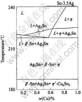
ͼ5 ��Thermo-Calc�����Sn-3.5Ag-xCu��ͼ
Fig.5 Phase diagram of Sn-3.5Ag-xCu calculated by Thermo-Calc
3 ����
1) ����ʱЧ100h��, Sn-3.5Ag-0.5Cu/Cu�������Cu6Sn5��Cu3Sn��������仯����, ����-����ѭ����720��ʱ, ������ֻ��Cu6Sn5��, û������Cu3Sn�� ԭ�������ڼ���Ӧ��Ӧ��ѭ����Ӱ��, Cu6Sn5���������ڹ���ȱ��, Ϊ������Cu����ɢ�ṩ��ͨ����
2) ��-����ѭ���ͺ���ʱЧ������, �����仯����ij�ʼ��̬��Ϊ�ȱ�״, ���������ƽ��, ����Բ�״��ʽ������ ���ڽ������, ��-����ѭ��ʱЧ�����״Ag3Sn�ۼ�����Ϊ��״, ����ʱЧ��û�г��ִ�������
REFERENCES
[1]������, ������. Sn-Agϵ������Ǧ��ǥ�ϵij������о�[J]. ���ӹ��ռ���, 2002, 23(1): 7-9.
LIU Xiao-bo, WANG Guo-yong. Over-potential of Sn-Ag system electronic solders[J]. Electronics Process Technology, 2002, 23(1): 7-9.
[2]He M, Lau W H, Qi G J, et al. Intermetallic compound formation between Sn-3.5Ag solder and Ni-based metallization during liquid state reaction[J]. Tin Solid Flims, 2004, 462-463: 376-383.
[3]Zeng K, Tu K N. Six cases of reliability study of Pb-free solder joints in electronlic packaging technology[J]. Materials Science and Engineering R, 2002, 38: 55-105.
[4]Pang J H L, Low T H, Xiong B S, et al. Thermal cycling aging effects on Sn-Ag-Cu solder joint micr-ostructure, IMC and strength[J]. Thin Solid Flims, 2004, 462-463: 370-375.
[5]��Ծ, ����, ����. ��Ǧ��ǥ�ϵ��о�[J]. �㶫��ɫ����ѧ��, 1998, 8(2): 99-105.
ZHAO Yue, DU Kun, HU Zhen. Study on lead-free solder[J]. Journal of Guangdong Nonferrous Metals, 1998, 8(2): 99-105.
[6]Prakash K H, Sritharan T. Interface reaction between copper and molten Tin-lead solders[J]. Acta Mater, 2001, 49: 2481-2489.
[7]������, �ڴ�ȫ, ����, ��. Sn-6Bi-2Ag(Cu, Sb)��Ǧǥ�ϺϽ�����֯����[J]. �й���ɫ����ѧ��, 2002, 12(3): 486-490.
HUANG Ming-liang, YU Da-quan, WANG Lai, et al. Microstructures of Sn-6Bi-2Ag(Cu, Sb) lead-free solder alloys[J]. The Chinese Journal of Nonferrous Metals, 2002, 12(3): 486-490.
[8]���캵, ����Ⱥ, ���»�. Sn-Ag-Cuϵ��Ǧ�����ɷֵ��Ż��о�[J]. ����Ԫ�������, 2004, 23(8): 14-16, 21.
XU Tian-han, ZHAO Mai-qun, LIU Xin-hua. Study on the optimal lead-free solder alloy of Sn-Ag-Cu system[J]. Electronic Components and Materials, 2004, 23(8): 14-16, 21.
[9]Luo W C, Kao C R. Liquid/solid and solid/solid reactions between SnAgCu lead-free solders and Ni surface finish[A]. Proceedings of the 4th International Symposium on Electronic Materials and Packaging[C]. Piscataway, NJ: IEEE, 2002. 330-334.
[10]����, �Խ�, ����, ��. ���庸����������Ǧ������֯�ݱ���ɵ��о�[J]. ���ӹ��ռ���, 2004, 25(2): 64-67.
QI Lin, ZHAO Jie, WANG Lai, et al. Microstructure evolution in lead-free solder joints after wave soldering and reflow soldering[J]. Electronics Process Technology, 2004, 25(2): 64-67.
[11]QI Lin, ZHAO Jie, WANG Xiu-min, et al. The effect of Bi on the IMC growth in Sn-3Ag-0.5Cu solder interface during aging process[A]. Proceedings of 2004 International Conference on the Business of Electronic Product Reliability and Liability[C]. Shanghai: Institute of Electrical and Electronics Engineering Inc, 2004. 42-46.
[12]Yoon J W, Jung S B. Effect of isothermal aging on intermetallic compound layer growth at the interface between Sn-3.5Ag-0.75Cu solder and Cu substrate[J]. Journal of Materials Science, 2004, 39(13): 4211-4217.
[13]Ahat S, �����, ��־��, ��. SnAgCu������װ������ʱЧ����ѭ�������е���֯������ǿ�ȱ仯[J]. ����ѧ��, 2001, 37(4): 439-444.
Ahat S, DU Li-guang, SUN Zhi-guo, et al. Effects of aging and thermal cycling on the microstructure and shear strength of SnAgCu surface mount solder joint[J]. Acta Metallurgica Sinica, 2001, 37(4): 439- 444.
[14]Vianco P T, Rejent J A, Hlava P F. Solid-state intermetallic compound layer growth between copper and 95.5Sn-3.9Ag-0.6Cu solder[J]. Journal of Electronic Materials, 2004, 33(9): 990-1004.
[15]Ahat S, Sheng M, Luo L. Effects of static thermal aging and thermal cycling on the microstructure and shear strength of Sn/sub 95.5/Ag/sub 3.8/Cu/sub 0.7/solder joints[J]. Journal of Materials Research, 2001, 16(10): 2914-2921.
[16]Kim K S, Huh S H, Suganuma K. Effects of intermetallic compounds on properties of Sn-Ag-Cu lead-free soldered joints[J]. Journal of Alloys and Compounds, 2003, 352: 226-236.
������Ŀ: ������Ȼ��ѧ����������Ŀ(50371010)
�ո�����: 2005-07-11; ������: 2005-09-27
�����: �� ��(1980-), Ů, ˶ʿ
ͨѶ����: �Ƽ̻�, ����; �绰: 010-62334859; E-mail: jihuahuang47@sina.com
[1]������, ������. Sn-Agϵ������Ǧ��ǥ�ϵij������о�[J]. ���ӹ��ռ���, 2002, 23(1): 7-9.
[5]��Ծ, ����, ����. ��Ǧ��ǥ�ϵ��о�[J]. �㶫��ɫ����ѧ��, 1998, 8(2): 99-105.
[8]���캵, ����Ⱥ, ���»�. Sn-Ag-Cuϵ��Ǧ�����ɷֵ��Ż��о�[J]. ����Ԫ�������, 2004, 23(8): 14-16, 21.
[10]����, �Խ�, ����, ��. ���庸����������Ǧ������֯�ݱ���ɵ��о�[J]. ���ӹ��ռ���, 2004, 25(2): 64-67.
