
Article ID: 1003-6326(2005)02-0332-04
High electron mobility of modulation doped GaAs after growing InP by solid source molecular beam epitaxy
SHU Yong-chun(������)1, PI Biao(Ƥ ��)1, LIN Yao-wang(��ҫ��)1, 2,
XING Xiao-dong(��С��)1, YAO Jiang-hong(Ҧ����)1,
WANG Zhan-guo(��ռ��)1, 2, XU Jing-jun(������)1
(1. Key Laboratory of Advanced Technique and Fabrication forWeak-Light Nonlinear Photonics Materials,
Ministry of Education, Nankai University, Tianjin 300457, China;
2. Key Laboratory for Semiconductor Materials Science, Chinese Academy of Sciences, Beijing 100083, China)
Abstract:
Modulation-doped AlGaAs/GaAs structures were grown on GaAs(100) substrate by solid source molecular beam epitaxy(SSMBE) system. The factors which influence the electron mobility were investigated. After growing InP based materials, growth conditions were deteriorated, but by an appropriate method and using reasonable process high electron mobility(77K) of more than 1.50��105cm2/(V��s) can still be obtained. The structures and growth conditions have been studied and optimized via Hall measurements. For a typical sample, 2.0K electron mobility as high as 1.78��106cm2/(V��s) is achieved, and the quantum Hall oscillation phenomena can be observed.
Key words:
modulation doped GaAs; high electron mobility; quantum Hall oscillation CLC number: TN386; TN385;
Document code: A
1 INTRODUCTION
Modulation doping produced high-mobility two dimensional electron gas(2DEG) in the AlGaAs/GaAs heterointerface by the physical separation of free electrons from positively ionized mother donors[1, 2]. Modulation doped heterostructure have attracted much interest for high-speed devices[3-5], low-noise microwave amplifiers[6] and for millimeter-wave integrated circuits(MMICs)[7] because of the extremely high mobility of two dimensional electron gas accumulating at the heterojunction interface. The high quality heterostructure materials have been achieved by molecular beam epitaxy(MBE). MBE makes abrupt doping profile and abrupt heterojunction interface in the materials possible, resulting in the surprising high mobility of 2DEG at low temperatures because of the nearly ideal spatial separation between electron and their parent ionized donors. The novel lasers and photo detectors can be integrated monolithically with GaAs integrated circuit to form opto-electronic integrated circuits(OEICs) which are very important in application[8].
The factors to limit electron mobility in a modulation doped GaAs are as follows[9, 10]: 1) remote impurity scattering by the ionized donors in the doped AlGaAs layer; 2) background impurity scattering from centers in the undoped GaAs and in the undoped AlGaAs spacer; 3) acoustic phonon scattering; 4) scattering at the GaAs-AlGaAs interface caused by surface roughness, alloy composition change or interface changes. The effect of scattering mechanism on electron mobility of modulation doped GaAs under different conditions is quite different.
The growth of phosphorus-contained materials by molecular beam epitaxy using solid-state phosphorus source is a good choice not only for environmental consideration but also device application. Reproducible growth of quantum well lasers with excellent performance[11, 12] and InGaP/GaAs heterostructure bipolar transistor(HBT) with a high yield[13, 14] are demonstrated by SSMBE.
In the molecular beam epitaxy system, the effect after growing phosphor-contained materials on the growth and electron mobility of modulation doped GaAs are very attractive. After growing phosphor-contained(P-contained) materials, the residual P may substrate As during epitaxial growth as equivalent electron doping. Even though the electron amounts in atomic outer space of As and P are equal, coulomb forces between ions and electrons in As and P are quite different. GaAsP/GaAs formed by equivalent electron doping may produce a tensile strain[15] which is beneficial to increasing the roughness of interface AlGaAs/GaAs in MD-GaAs. Both effects above may cause a decrease of electron mobility of MD-GaAs at 77K. In this paper, an investigation on high electron mobility of modulation doped GaAs grown by SSMBE system is investigated. The factors which influence the electron mobility have been studied. After growing P-contained materials, growth conditions were deteriorated seriously; but high electron mobility at 77K more than 1.50��105cm2/(V��s) can still be obtained by using an appropriate method. The structures and growth conditions have been studied and optimized via Hall measurements. For a typical sample, 2K electron mobility as high as 1.78��106cm2/(V��s) can be achieved, and the quantum Hall oscillation phenomena can be observed.
2 EXPERIMENTAL
In this experiment, the growth of modulation doped GaAs structure materials was carried out in a Riber Compact 21 MBE system equipped with Riber VAC 500 arsenic(As) valve cracker cell and a Riber KPC250 phosphorus(P) cracker cell. The purities of As and P charge used were 7N5 and 7N (Nine), respectively, supplied by Rasa Industries of Japan. The purities of gallium and aluminum charge used are 7N and 6N5 respectively supplied by GEO and Pechiney of France. Silicon charge used for dopant is 4500����cm made in China.
The semi-insulating GaAs substrates oriented(100) were made in China. In order to reduce the background impurities of the epitaxial layers, before and after loading source materials, the MBE system has to be baked (at 200�� for 300h), and source cells and materials have to be degassed thoroughly.
As cracker zone temperature was fixed at 600�� and bulk evaporator temperature was fixed at 330��, the beam equivalent pressure of As(BEPAs) was precisely adjusted by controlling the valve opening of As cracker cell using an automatic position controller. The growth rates of GaAs and AlGaAs were 0.72 and 1.0��m/h, respectively, As4/Ga BEP ratio was between 10 and 15. The growth chamber without cooling by liquid nitrogen reached a pressure of 1.1��10-10Pa, as the source cells were at idle temperatures. The growth chamber is cooled by liquid nitrogen and reached a pressure of 2.6��10-8Pa before growth run.
The sketch diagram of modulation doped GaAs structure is shown in Fig.1. It consists of a 55nm-thick Si-doped AlxGa1-xAs layer(x=0.28) with doping concentration of 1.0��1018cm-3, an undoped AlxGa1-xAs spacer-layer with thickness of 16-25nm, and a 1.20��m-thick undoped GaAs layer. 2DEG is formed at the GaAs side of heterojunction interface. AlAs mole fraction(x) of 0.28 was chosen for considering the persistent photo conduction(PPC) effect in the sample due to higher value of x with Si doping to form DX center. As is well known, AlAs mole fraction(x) as high as 0.37 was reported[16, 17], but a delta-doping with Si has been used at the structures[18, 19]. The experimental results of the structure with Si delta-doping will be reported in another paper.
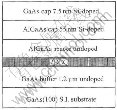
Fig.1 Structure modulation doped GaAs
3 RESULTS AND DISCUSSION
Fig.2 shows the plot of electron mobility and concentration of modulation doped GaAs at 77K as a function of spacer thickness. As it can be seen from Fig.2 that, when the spacer thickness increases, the electron concentration reduces gradually, but the mobility appears to be in different variation. When the spacer increases from 16nm to 22nm, the mobility increases from 1.6��105 to 1.86��105cm2/(V��s). The mobility reaches a peak value at the thickness of 22nm. The mobility reduces significantly as the spacer thickness is higher than 22nm. In order to analyze these data above, the different possible scattering mechanisms have been taken into account. As the thickness is less than 22nm, the remote ionization impurities in the doped AlGaAs dominate the scattering and an increase in spacer thickness produce increase mobility. However, for larger spacers(�� 22nm), the background impurities in the undoped GaAs, undoped AlGaAs spacer dominate the scattering, and since mobility can be shown to vary as n3/2[17]. The fall in carrier concentration(n) will produce a reduction in 77K mobility[19]. It is clear that the more carrier concentration can be beneficial to shield carrier transport from ionized background impurities.
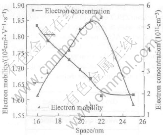
Fig.2 Electron mobility and concentration of modulation doped GaAs at 77K as function of spacer thickness
Fig.3 shows the dependence of growth temperature on 77K electron mobility of modulation doped GaAs. As seen in Fig.3, the highest electron mobility at 77K of modulation doped GaAs was grown at the growth temperature of 710��. The higher growth temperature may cause. As adsorptions which is not beneficial for stoichiometric growth. The lower growth temperature may lead to increasing Ga(Al) vacancies or the roughness of AlGaAs/GaAs interface that would cause a decrease of electron mobility.
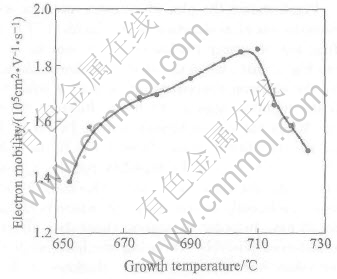
Fig.3 Dependence of growth temperature on electron mobility of modulation doped GaAs at 77K
Table 1 shows the 77K electron concentration and mobility of modulation doped GaAs grown before and after growing P-contained materials. It can be seen from Table 1 that before growing P-contained materials, the 77K electron mobility reaches 1.62��105cm2/(V��s) easily, and after growing a series of P-contained materials, growth conditions were deteriorated seriously, an appropriate method was used for suppressing the influence caused by using phosphorus solid source. The modulation doped GaAs was grown once again, the 77K electron mobility reached 1.58��105cm2/(V��s) at the beginning. Then the material structure and growth conditions have been optimized via the results of Hall measurements. The 77K electron mobility increases to 1.85��105cm2/(V��s). For a typical sample, after illuminated the 77K electron mobility reaches as high as 2.35��105cm2/(V��s), and the 2.0K electron mobility as high as 1.78��106cm2/(V��s) has been achieved, and the quantum hall oscillation phenomena can be observed(Fig.4). Fig.4 shows the illuminated results for Rxx (Shubnikovde Haas effect) and Rxy(Integral Hall effect) of the 2DEG as a function of magnetic field at a temperature of 2.0K. In the vicinity of 2.8T and 4.1T, Rxx approaches the zero-resistance state. At these same field positions, Rxy develops plateaus characteristic of the integral quantum Hall effect (IQHE). All features reflected the high quality of the 2DEG very clearly. The results above demonstrate that the high quality MD-GaAs materials can still be obtained after growing P-contained materials.

Fig.4 Shubnikovde Haas effect and integral Hall effect of illuminated sample L037 at temperature of 2.0K
Table 1 Electron concentration and mobility before and after growing P-contained materials at 77K

In order to characterize modulation doped two-dimensional electron gas(2DEG) structure, the quantum Hall measurements have been carried out at low temperature in high intensity magnet field[7]. Fig.4 shows the dependence of magneto-resistance of modulation doped 2DEG structure on the intensity of magnet field at temperature of 2.0K, with electrical current 0.12��A. As seen in Fig.4, the amplitude and shape of quantum Hall oscillation curve does not depend on electrical current, but on the irradiation, especially when the intensity is higher than 5T.
4 CONCLUSIONS
After growing P-contained materials, growth conditions were deteriorated, but using appropriate method to suppress the influence after growing P-contained materials, high electron mobility (77K) more than 1.50��105cm2/(V��s) can still be obtained. The structures and growth conditions have been studied and optimized via Hall measurements. For a typical sample, 2.0K electron mobility as high as 1.78��106cm2/(V��s) has been achieved, and the quantum Hall oscillation phenomena can be observed.
ACKNOWLEDGEMENT
The authors would like to thank L�a Li, WANG Wan-nian, WANG Yu-tian, ZHANG Xiu-lan for electronic characterization of modulation doped GaAs. This work was supported by TEDA College of Nankai University.
REFERENCES
[1]Saku T, Hirayama Y, Horikoshi Y. High electron mobility in AlGaAs/GaAs modulation-doped structures [J]. Jpn J Appl Phys, 1991, 30(5): 902-905.
[2]Sahu T, Patnaik J. Electron transport mobility in a ��-doped double quantum well structure [J]. J Appl Phys, 2000, 88(5): 2658-2664.
[3]Meier C, Reuter D, Riedesel C, et al. Fabrication of two-dimensional electron system by focused ion beam doping of ��/�� semiconductor heterostructures [J]. J Appl Phys, 2003. 93(10): 6100-6106.
[4]Triplett G, May G, Brown A. Modeling electron mobility in MBE-grown InAs/AlSb thin films for HEMT applications using neural networks [J]. Solid-State Electronics, 2002, 46(10): 1519-1524.
[5]Lee C S, Hsu W C, Li S S, et al. A d-doped In0.24Ga0.76As/GaAs pseudomorphic high electron mobility transistor using a superlattice spacer [J]. Superlattices and Microstructrue, 2001, 29(5): 329-334.
[6]Anholt R. Quantum mechanics prescriptions for compound semiconductor transistor technologies [J]. Solid-State Electronics, 2001, 45: 1189-1197.
[7]Cho A Y. Twenty years of molecular beam epitaxy [J]. J of Crystal Growth, 1995, 50: 1-6.
[8]Cho A Y, Sivco D L, Ng H M, et al. Quantum devices, MBE technology for the 21st century [J]. Journal of Crystal Growth, 2001, 227-228: 1-7.
[9]Mazon K T, Hai G Q, Lee M T, et al. Low-temperature clectron mobilities due to ionized-impurity scattering in multisubband two-dimensional semiconductor systems [J]. Phys Rev B, 2004, B70(19): 193312.
[10]YANG Bin, CHENG Yong-hai, WANG Zhan-guo, et al. Interface roughness scattering in GaAs-AlGaAs modulation-doped heterostructures [J]. Appl Phys Lett, 1994, 65(26): 3329-3331.
[11]Klopf F, Reithmaier J P, Forchel A. Highly efficient GaInAs/(Al)GaAs quantum-dot lasers based on a single active layer versus 98nm high-power quantum-well lasers [J]. Appl Phys Lett, 2000, 77(10): 1419-1421.
[12]Chu S N G, Chand N, Joyce W B, et al. Generic degradation mechanism for 98nm InxGa1-xAs/GaAs strained quantum-well lasers [J]. Appl Phys Lett, 2001, 78(21): 3166-3168.
[13]Wilk A, Zaknoune M, Godey S, et al. Growth of Be-doped GaInP/GaAs heterostructure bipolar transistor by all solid-source multiwafer production molecular beam epitaxy [J]. J Vac Sci Technol B, 2004, 22(3): 1-6.
[14]Li W, Likonen J, Haapamaa J, et al. Study of concentration-dependent Be diffusion in GaInP layers grown by gas source molecular beam epitaxy [J]. J Appl Phys, 2000, 87: 7592.
[15]Kuznetssov M, Hakimi F, Sprague R, et al. Design and characteristics of high-power (-0.5-W CW) diode-pumped vertical-external-cavity surface-emitting semiconductor lasers with circular TEM00 beams [J]. IEEE J of Selected Topics in Quantum Electronics, 1999, 5(3): 561-573.
[16]Umansky V, De-picciotto R, Heiblum M. Extremely high-mobilty two dimensional electron gas: Evaluation of scattering mechanisms [J]. Appl Phys Lett, 1997, 71(5): 683-685.
[17]Saku T, Horikoshi Y, Tokura Y. Limit of electron mobility in AlGaAs/GaAs modulation-doped heterostructures [J]. Jpn J Appl Phys, 1996, 35: 34-37.
[18]Foxon C T, Harris J J, Hilton D, et al. Optimisation of (Al/Ga)As/GaAs two-dimensional electron stucture for two carrier densities and ultrahigh mobility at low temperatures [J]. Semicond Sci Technol, 1989, 4: 582-585.
[19]Reuter D, Versen M, Schneider M D , et al. Increased mobility anisotropy in selectively doped AlxGa1-xAs/GaAs heterostructures with electron densities [J]. J Appl Phys, 2000, 88(1): 321-325.
Received date: 2004-11-20; Accepted date: 2005-01-18
Correspondence: SHU Yong-chun, Professor; Tel: +86-22-66229609; E-mail: shuyc@nankai.edu.cn
