
Thermal performance of sputtered Cu films containing insoluble Zr and Cr for advanced barrierless Cu metallization
WANG Xin-jian(���½�), DONG Xian-ping(����ƽ), JIANG Chuan-hai(������)
School of Materials Science and Engineering, Shanghai Jiao Tong University, Shanghai 200240, China
Received 29 December 2008; accepted 4 May 2009
Abstract:
Pure Cu films and Cu alloy films containing insoluble substances (Zr and Cr) were deposited on Si(100) substrates, in the presence of interfacial native suboxide (SiOx), by magnetron sputtering. Samples were vacuum annealed between 300 �� and 500 �� to investigate effects of Zr and Cr additions on the thermal performance of Cu films. After annealing, copper silicides were found in the Cu(Zr) films, while no detectable silicides were observed in Cu and Cu(Cr) films. Upon annealing, Zr accelerated the diffusion and reaction between the film and the substrate, and lowered the thermal stability of Cu(Zr) alloy films on Si substrates, which was ascribed to the ��purifying effect�� of Zr on the Si substrates. Whereas, Cr prohibited the agglomeration of Cu films at 500 �� and decreased the surface roughness. As a result, the diffusion of Cu in Si substrates for Cu(Cr) films was effectively inhibited. In contrast to the high resistivity of Cu(Zr) films, the final resistivity of about 2.76 �̦�?cm was achieved for the Cu(Cr) film. These results indicate that Cu(Cr) films have higher thermal stability than Cu(Zr) films on Si substrates and are preferable in the advanced barrierless Cu metallization.
Key words:
copper film; barrierless metallization; magnetron sputtering, thermal stability; purifying effect;
1 Introduction
Cu interconnects have replaced Al alloy ones in the advanced metallization because of their reduced resistance-capacitance circuit (RC) delay[1-2]. However, there are many problems that must be addressed in Cu metallization. Historically, the key issue is its fast diffusion into the surrounding dielectric layers[3]. In addition, the adhesion of Cu films to Si and SiO2 substrates and the surface roughness of Cu films are equally important technical problems to be resolved[3-4]. Conventionally, a diffusion barrier such as TiN or TaN is used to solve these problems[5]. However, recent efforts have been focused on enhancing the thermal stability of Cu films in the Si-based barrierless scheme because of the shrinking feature size of interconnects. Doping Cu with insoluble elements is one of the barrierless metallization schemes to slow down the interaction between Cu and Si[5-7]. Because these Cu alloy films have relatively low resistivities than the conventional barrier layers, it is advantageous to using these films as seed layers directly on barrierless Si substrates. Nevertheless, Cu alloy films, to be used as seed layers, are demanded to have the comparable thermal stability with the conventional diffusion barriers. It is a pity that some studies have reported a nonmonotonic influence of alloying addition on the thermal stability of Cu films[8-9]. In the current study, we chose Zr and Cr as the alloying elements, in view of the following favorable points. First, Zr and Cr can precipitate out of the Cu matrix after annealing at around 400 ��, decreasing the resistivities of alloy films on SiO2 substrates[10-11]. Second, Cu(Zr) and Cu(Cr) films have improved properties, such as good adhesion with SiO2, high electromigration resistance and mechanical properties [11-14]. Therefore, it is of great interest to examine the thermal stability of Cu films containing insoluble Zr and Cr on Si substrates, in the presence of interfacial native suboxide (SiOx). The results presented here are expected to provide a useful reference for the selection of alloy films for the advanced barrierless schemes.
2 Experimental
Cu-Zr films and Cu-Cr films were deposited on Si(100) substrates by magnetron sputtering a pure Cu (99.99%) target inlaid with Zr sticks (99.9%) or Cr sticks (99.9%) in a chamber with a base pressure less than 2��10-4 Pa. More information about the preparation of alloy films has been reported previously[15]. For comparison, pure Cu films were prepared under the same condition. The silicon wafers were successively cleaned in trichloroethylene and acetone, followed each time by deionized water rinsing. Because the substrates were not etched with hydrofluoric acid (HF), there was a native suboxide (SiOx) layer of about 15 ? thick on the surface [16]. The sputtering power and working pressure for the film deposition were 100 W and 0.67 Pa, respectively. The composition of films was determined to be Cu-2.2%Zr and Cu-2.6%Cr (molar fraction), respectively. The film thickness was about 300 nm, measured by a surface profile meter. Samples were then vacuum- annealed in a temperature range of 300-500 �� for 60 min, at a pressure of (2-3)��10-3 Pa.
X-ray diffractometer(XRD) was used for the crystallographic characterization of films. Cross- sectional morphologies and the surface roughness were obtained by field emission scanning electron microscopy (FESEM) and atomic force microscopy(AFM). The AFM measurement was performed in tapping mode with 256��256 data collected over an area of 5 ��m��5 ��m and a scan speed of 2 Hz. The compositional depth profile and interfacial characteristic analysis were performed by Auger electron spectroscopy(AES). The resistivity as a function of the annealing temperature was measured by four-point probe method.
3 Results and discussion
3.1 Film crystallography and morphologies
The XRD patterns of Cu(Zr)/SiOx/Si and Cu(Cr)/ SiOx/Si samples are shown in Fig.1 and Fig.2, respectively. For comparison, XRD pattern of the 500 ��- annealed Cu/SiOx/Si sample is also shown. Both alloy films exhibited Cu diffraction peaks and no diffraction peaks corresponding to Zr or Cr precipitates were observed in the as-deposited state. The evidently broadened Brag peaks confirmed the ion mixing, which resulted in the refinement of film structure. After annealing, no obvious copper silicides were found for the Cu and Cu(Cr) films. According to the result in Ref.[6], the absence of copper silicides in the Cu/SiOx/Si system annealed below 500 �� might be due to the presence of interfacial native SiOx layer. By comparison, copper silicides (Cu3Si and Cu4Si) appeared after annealing at temperatures as low as 300 �� for the Cu(Zr) film, which indicated that Zr additives accelerated the diffusion and reaction between Cu and Si at the interface for the Cu(Zr)/SiOx/Si system. However, peaks of Cu4Si phase disappeared at higher temperatures, implying that Cu3Si was more stable than Cu4Si at high temperatures. Compared with the other two systems, Cu(200) peak intensity in the XRD spectra of the Cu(Cr)/SiOx/Si system was particularly low (Fig.2). This indicated that addition of Cr promoted the (111) texture evolution in the Cu(Cr) films. These results reveal that the Cu(Cr)/SiOx/Si system had much higher thermal stability than Cu/SiOx/Si and Cu(Zr)/ SiOx/Si systems upon annealing.
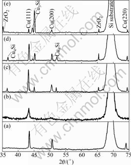
Fig.1 XRD patterns of 500 ��-annealed Cu/SiOx/Si (a) and Cu(Zr)/SiOx/Si samples before and after annealing at different temperatures ((b) As-deposited; (c) 300 ��; (d) 400 ��; (e) 500 ��)
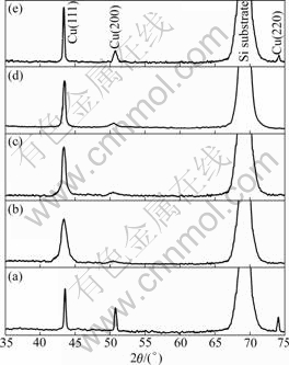
Fig.2 XRD patterns of 500 ��-annealed Cu/SiOx/Si (a) and Cu(Cr)/SiOx/Si samples before and after annealing at different temperatures ((b) As-deposited; (c) 300 ��; (d) 400 ��; (e) 500 ��)
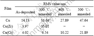
Fig.3 shows the cross-sectional FESEM images of the investigated samples before and after annealing. The surface roughness RMS (root mean square) values have been obtained by AFM, which are listed in Table 1. A columnar structure could be observed in the as-deposited Cu film. However, the poor textured Cu film took a significant fraction of regions with equiaxed grains near the film surface. Distinctly, the typical columnar structure of Cu(Zr) and Cu(Cr) films appeared to be much finer than that of the Cu film. The RMS values decreased from 14.13 nm for the Cu film to 3.97 nm and 4.02 nm for the Cu(Zr) and Cu(Cr) films in the as-deposited state, respectively. This suggested that Zr or Cr atoms mixed with Cu atoms and prevented the Cu grain growth on the surface of films. After annealing at 400 ��, with the coalescence and extensive growth of crystallites/grains taking place, the columnar structure in the Cu film disappeared completely. Meanwhile, many pinholes were formed on the film surface. The coarsened Cu grains might induce the grooving process and produce pinholes on the surface. As a result, the surface undulation was increased, with a RMS value of about 27.89 nm. After further heating up to 500 ��, part of these neighboring pinholes coalesced and merged, forming large holes in the film, which was considered to be driven by the minimization of interface energy. The coalescence of Cu films, perpendicular to the film surface, resulted in the great roughness of Cu/SiOx/Si samples[16]. However, the Cu(Zr) film was nearly ruptured after annealing at 400 �� for 60 min. Note that some tubercles were grown inside the Si substrate. Although the composition could not be identified exactly because of the small size, these tubercles might be corresponded to the copper silicides, as indicated by XRD. The similar result had been reported in Ref. [7]. As a result, the surface roughness of films increased sharply so that the RMS values could not be measured accurately. In contrast, despite the aggregated crystallites, the Cu(Cr) films appeared to be more continuous and compact than Cu and Cu(Zr) films after annealing. Moreover, the film surface and interface were much smoother and flatter, suggesting that Cu(Cr) films had the better wettability on the Si substrates than the other two films. The RMS values of Cu(Cr) films after annealing at 400 �� and 500 �� were 10.22 nm and 21.89 nm, respectively. These results confirmed that Cr prohibited the Cu agglomeration at 500 �� and enhanced the thermal stability of Cu(Cr) films markedly, while adding Zr to Cu films aggravated the diffusion and reaction between the film and the substrate.
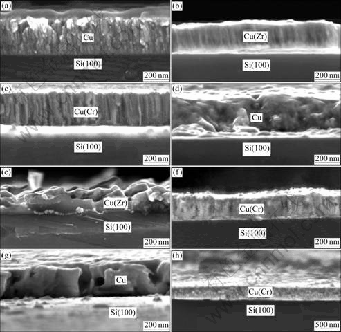
Fig.3 Cross-sectional FESEM images of Cu (a, d, g), Cu(Zr) (b, e,), and Cu(Cr) (c, f, h) films: (a), (b), (c) As-deposited; (d), (e), (f) Annealed at 400 ��; (g), (h) Annealed at 500 ��
Therefore, the Cu(Cr) alloy film is rather stable and can keep a smooth surface at the processing temperature (about 400 ��) in silicon-large scale integrated circuits (Si-LSICs).
3.2 Interfacial diffusion and reaction characteristics
Fig.4 shows the AES depth profiles of 400 ��- annealed samples. The vertical axis represents the Auger electron intensity, corresponding to the relative concentration of constituting elements. The horizontal axis represents the sputtering time. The results revealed strong intensity of alloying elements (Zr or Cr) on the film surface, indicating that both Zr and Cr had segregated on the surface. Note that the intensity profiles of Si, O and alloying elements in the interior of Cu(Cr) films were of background level, showing that the concentrations of these elements were below the detection limit of AES. However, the intensity of Si in Cu and Cu(Zr) films was higher than that in Cu(Cr) films, indicating that Si had diffused into the films. Meanwhile, a more shallow diffusion depth of Cu in Si substrates was found in the Cu(Cr)/SiOx/Si sample than in the other samples.
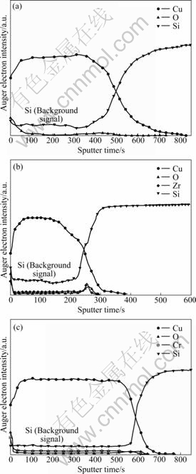
Fig.4 AES compositional depth profiles of Cu/SiOx/Si (a), Cu(Zr)/SiOx/Si (b) and Cu(Cr)/SiOx/Si (c) samples after annealing at 400 ��
To further investigate the film/substrate interface, we have stripped the overlayers of 400 ��-annealed Cu/SiOx/Si, Cu(Zr)/SiOx/Si and Cu(Cr)/SiOx/Si samples by chemical solution (mixture of nitric acid, phosphoric acid, and acetic acid), and analyzed the exposed substrate surfaces by AES (Fig.5). Obvious Zr and Cr signals were observed for the alloy films, suggesting that Zr and Cr had indeed segregated at the interfaces after annealing. Additionally, much stronger Cu signal was found for the Cu(Zr)/SiOx/Si sample, while no obvious Cu signal wasdetected for the Cu(Cr)/SiOx/Si sample. The results confirmed that when annealing at 400 ��, the diffusion of Cu into the substrate for the Cu(Zr)/SiOx/Si system was very serious, while it was effectively prohibited for the Cu(Cr)/SiOx/Si system, which may be related with the fine structure of the film and the segregation of Cr.
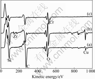
Fig.5 Auger survey spectra of substrate surfaces after etching overlayers for 400 ��-annealed Cu/SiOx/Si (a), Cu(Zr)/SiOx/Si (b) and Cu(Cr)/SiOx/Si (c) samples
The strong reaction between Cu and Si in Cu(Zr)/ SiOx/Si system is interesting and can be intimately related to the bonding at the interface. Just as mentioned above, upon annealing, the interfacial oxygen adatoms,which were bonded with Si to form a native suboxide (SiOx) layer, inhibited the reaction between Cu and Si at lower temperatures (��500 ��). In the presence of Zr atoms, owing to the much lower standard free energy of formation![]() of ZrO2 (about -970 kJ/mol) than that of SiO2 (about -780 kJ/mol) at 400 ��[17], Zr atoms had a strong tendency to break the neighboring Si��O bonds to form the more stable oxide layer (ZrO2) at the interface. However, the ZrO2 layer was not continuous and thick enough to prohibit the diffusion and reaction between Cu and Si because of the little oxygen content. As a result, the outmost exposed fresh Si reacted with Cu at a very low temperature (��300��), which was in good agreement with previous work[18-19]. We call this ��purifying effect��, which is somewhat opposite to the ��catalytic effect�� of interfacial Cu in the oxidation of Si[20]. It is the ��purifying effect�� of Zr that accelerated the reaction between the Cu(Zr) film and the substrate. In contrast, with high
of ZrO2 (about -970 kJ/mol) than that of SiO2 (about -780 kJ/mol) at 400 ��[17], Zr atoms had a strong tendency to break the neighboring Si��O bonds to form the more stable oxide layer (ZrO2) at the interface. However, the ZrO2 layer was not continuous and thick enough to prohibit the diffusion and reaction between Cu and Si because of the little oxygen content. As a result, the outmost exposed fresh Si reacted with Cu at a very low temperature (��300��), which was in good agreement with previous work[18-19]. We call this ��purifying effect��, which is somewhat opposite to the ��catalytic effect�� of interfacial Cu in the oxidation of Si[20]. It is the ��purifying effect�� of Zr that accelerated the reaction between the Cu(Zr) film and the substrate. In contrast, with high![]() (about -650 kJ/mol) of Cr2O3, Cr could not deprive of the interfacial oxygen adatoms. As a result, the fine structure of films and the segregation of Cr at the surface and interface enhanced the thermal stability of the Cu(Cr)/SiOx/Si system.
(about -650 kJ/mol) of Cr2O3, Cr could not deprive of the interfacial oxygen adatoms. As a result, the fine structure of films and the segregation of Cr at the surface and interface enhanced the thermal stability of the Cu(Cr)/SiOx/Si system.
3.3 Resistivity
Fig.6 shows the comparison of the resistivities of Cu, Cu(Zr) and Cu(Cr) films before and after annealing. The as-deposited Cu(Zr) and Cu(Cr) alloy films had higher resistivities than Cu films because of the impurity effect of Zr and Cr as well as the refined grain structure. After annealing, the observation of the morphology was in good agreement with the resistivity result. An abrupt increase in resistivity of the Cu film occurred at 500 ��, which may be due to the agglomeration of the Cu film. In contrast, resistivities of Cu(Zr) films remained at high values all through the annealing temperature because of the thermal instability. However, the resistivities of Cu(Cr) films decreased with the increasing annealing temperature. The final resistivity was about 2.76 �̦�?cm after annealing at 500 �� for 60 min.
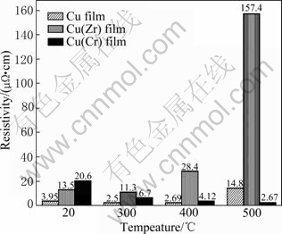
Fig.6 Variation of resistivity with annealing temperatures for Cu/SiOx/Si, Cu(Zr)/SiOx/Si and Cu(Cr)/SiOx/Si samples
Based on these results, the Cu films containing alloying element (M) used in the device for the future barrierless metallization should satisfy the following conditions: 1) the solubility limit of M in Cu should be small enough at room temperature; 2) the alloying element (M) should not decrease the melting temperature of Cu much; and 3) the oxide of alloying element (MOx) should have a higher free energy of formation ![]() than SiO2 at about 400 ��. Among them, rule 1) ensures that M can segregate out of the Cu matrix and result in a low resistivity of films after annealing. Rules 2) and 3) are important for the application of Cu alloy films for the barrierless scheme because the Cu alloy with a lower melting temperature may have an aggravated agglomeration phenomenon and cannot keep a smooth surface upon annealing.
than SiO2 at about 400 ��. Among them, rule 1) ensures that M can segregate out of the Cu matrix and result in a low resistivity of films after annealing. Rules 2) and 3) are important for the application of Cu alloy films for the barrierless scheme because the Cu alloy with a lower melting temperature may have an aggravated agglomeration phenomenon and cannot keep a smooth surface upon annealing.
In a word, with the low resistivity and high thermal stability, the low-alloyed Cu(Cr) film exhibits great potential to be used as a seed layer for the advanced barrierless metallization. However, more work is needed to investigate the microstructural evolution and properties of Cu(Cr) films, such as the mechanical property and electromigration resistance. Once the optimal Cr content and annealing process are determined, the Cu(Cr) alloy will be a promising metallization material for ULSI application.
4 Conclusions
1) Cu films containing insoluble Zr or Cr were prepared by magnetron sputtering on the Si substrates, in the presence of interfacial native suboxide (SiOx). Insoluble Zr and Cr atoms refined the columnar structure and decreased the surface roughness of as-deposited Cu films markedly.
2) After annealing, Cu films agglomerated on the Si substrates, resulting in the great surface roughness at 500 ��. Adding Cr to Cu films prohibited the agglomeration of films and mitigated the diffusion of Cu into the Si substrates, decreasing the surface roughness markedly. However, Zr additives accelerated the diffusion and reaction between the film and the substrate, lowering the thermal stability of the Cu(Zr)/SiOx/Si system.
3) After annealing, a low resistivity (about 2.76 �̦�?cm) could be obtained for the Cu(Cr) film. Therefore, the low alloyed Cu(Cr) film is a favorable candidate for barrierless metallization.
References
[1] HU C K, HARPER J M. Copper internationals and reliability [J]. Mater Chem Phys, 1998, 52: 5-16.
[2] KOIE Y S, INASE T S, TAKAYAMA S J. Temperature dependence of internal stress and crystal growth of dilute Cu alloy film [J]. Solid State Phenon, 2007, 127: 147-152.
[3] LANFORD W A, DING P J, WANG W, HYMES S, MURARKA S P. Alloying of copper for use in microelectronic metallization [J]. Mater Chem Phys, 1995, 41: 192-198.
[4] KO Y K, JANG J H, LEE S, YANG H J, LEE W H, REUCROFT P J, LEE J G. Effect of molybdenum, silver dopants and a titanium substrate layer on copper film metallization [J]. J Mater Sci, 2003, 38: 217-222.
[5] KWAK M Y, SHIN D H, KANG T W, KIM K N. Characteristics of TiN barrier layer against Cu diffusion [J]. Thin Solid Films, 1999, 339: 290-293.
[6] LIN C H, CHU J P, MAHALINGAM T, LIN T N, WANG S F. Sputtered copper films with insoluble Mo for Cu metallization: A thermal annealing study [J]. J Electron Mater, 2003, 32: 1235-1239.
[7] CHU J P, LIN C H. Thermal stability of Cu(W) and Cu(Mo) films for advanced barrierless Cu metallization: Effects of annealing time [J]. J Electron Mater, 2006, 35: 1933-1936.
[8] ZHAO B, KIM H, SHIMOGAKI Y. Effects of Ag addition on the resistivity, texture and surface morphology of Cu metallization [J]. Jpn J Appl Phy, 2005, 44: L1278-L1281.
[9] KIM H, KOSEKI T, OHBA T, OHTA T, KOJIMA Y, SATO H, SHIMOGAKI Y. Process design of Cu(Sn) alloy deposition for highly reliable ultra large-scale integration interconnects [J]. Thin Solid Films, 2005, 491: 221-227.
[10] LIU B, SONG Z X, XU K W. The effect of zirconium dopant on the properties of copper films [J]. Surf Coat Technol, 2007, 201: 5419-5421.
[11] CABRAL C Jr, HARPER J M E, HOLLOWAY K, SMITH D A, SCHAD R G. Preparation of low resistivity Cu-1at.%Cr thin film by magnetron sputtering [J]. J Vac Sci Technol, 1992, A10: 1706-1712.
[12] RUSSELL S W, RAFALSKI S A, SPREITZER R L, LI J, MOINPOUR M, MOGHADAM F, ALFORD T L. Enhanced adhesion of copper to dielectrics via titanium and chromium additions and sacrificial reactions [J]. Thin Solid Films, 1995, 262: 154-167.
[13] LI J, MAYER J W, COLGAN E G. Oxidation and protection in copper and copper alloy thin films [J]. J Appl Phys, 1991, 70: 2820-2827.
[14] IGARASHI Y S, ITO T S. Properties of copper-zirconium alloy interconnect [J]. J Vac Sci Technol, 1998, B16: 2745-2750.
[15] WANG Xin-jian, JIANG Chuan-hai, WANG Jia-min, HONG Bo. Preparation of CuCr films by magnetron sputtering single target [J]. The Chinese Journal of Nonferrous Metals, 2006, 16(11): 1876-1881. (in Chinese)
[16] BENOUATTAS N, MOSSER A, RAISER D, FAERBER J, BOUABELLOU A. Behaviour of copper atoms in annealed Cu/SiOx/Si systems [J]. Appl Sur Sci, 2000, 153: 79-84.
[17] Barin, Thermochemical data of pure substances, 3rd ed [M]. Weinheim: Wiley-VCH Verlag GmBH, 1995, 1880.
[18] CHANG Chin-an. Formation of copper silicides from Cu(100)/Si(100) and Cu(111)/Si(111) structures [J]. J Appl Phys, 1990, 67: 566-569.
[19] CROS A, ABOELFOTOH M O, TU K N. Formation, oxidation, electronic, and electrical properties of copper silicides [J]. J Appl Phys, 1990, 67: 3328-3336.
[20] AFORD T L, JAQUEZ E J, THEODORE N D, RUSSELL S W, DIALE M, ADAMS D, ANDERS S. Influence of interfacial copper on the room temperature oxidation of silicon [J]. J Appl Phys, 1996, 79: 2074-207.
Foundation item: Project(08520740200) supported by the Applied Materials Research and Development Fund of Shanghai, China
Corresponding author: DONG Xian-ping; Tel: +86-21-54747471; E-mail: xpdong@sjtu.edu.cn
DOI: 10.1016/S1003-6326(09)60124-2
(Edited by YANG Bing)


