

Microstructure and optical properties of
TiO2 thin films deposited at different oxygen flow rates
ZHAO Bao-xing(�Ա���), ZHOU Ji-cheng(�ܼ̳�), RONG Lin-yan(������)
School of Energy Science and Engineering, Central South University, Changsha 410083, China
Received 10 October 2009; accepted 14 December 2009
Abstract:
To research the influence of oxygen flow rate on the structural and optical properties of TiO2 thin film, TiO2 films on glass were deposited by reactive magnetron sputtering. The microstructure and optical properties were measured by X-ray diffractometry, AFM and UV-VIS transmittance spectroscopy, respectively. The results show that the films deposited at oxygen flow rate of 10 mL/min has the lowest roughness and the highest transmittance. The absorption angle shifts to longer wavelengths as oxygen flow rates increase from 5 to 10 mL/min, then to shorter ones as the oxygen flow rate increase from 10 to 30 mL/min. The band gap is 3.38 eV, which is nearly constant in the experiment. For the TiO2 thin films deposited at 10 mL/min of oxyge flow rate, there are nano-crystalline structures, which are suitable for anti-reflection (AR) coating in the solar cells structure system.
Key words:
TiO2 film; reactive magnetron sputtering; anti-reflection coating; solar cell;
1 Introduction
Most solar cells for practical use are prepared by Si single crystals, multi-crystals or amorphous materials. The most important problem of such Si solar cells is to increase conversion efficiency. In crystalline silicon solar cells, surface texturing is used to trap light, leading to an enhancement in optical path length by up to 4n2, where n is the refractive index of the active layer[1]. However, the reflectivity of these surfaces increases rapidly with the increase of the angle of the light incidence at the air/texture interface. A common solution is to use an anti-reflection (AR) coating based on the optical interface. For example, quarter wavelength transparent layers of SiOx, TiO2, ZnO, ITO or Si3N4 are regularly used as AR coating on Si[2].
Titanium dioxide (TiO2) thin films have a long history in silicon photovoltaic (PV) as AR coating[3]. The use of TiO2 thin films has many advantages, including their very good chemical resistance to the majority of chemicals used in the PV industry and their optimal refractive index for glass encapsulated silicon solar cells[4-5]. Among three crystalline phases (anatase, rutile, and brookite), in which TiO2 can exist, the anatase phase is desired in AR coating applications because of high refraction index and low extinction index[6]. Moreover, TiO2 films have numerous interesting applications in optical coatings, optical waveguides, photo-decomposition of environmental pollutants, solar cells and electronic devices[7-8]. Many different procedures for the preparation of TiO2 films were reported[9]. In addition, the properties of TiO2 thin films largely depend not only with the preparation techniques but also with the deposition conditions [10]. As to reactive magnetron sputtering method, the properties of TiO2 thin films are largely influenced by the oxygen flow rate. However, little research has been carried out at present. Hence, an attempt has been made in this work to study the effect of the oxygen flow rate on the structural, morphological and optical properties of TiO2 thin films.
2 Experimental
TiO2 films, with a thickness of ~200 nm, were deposited by reactive magnetron sputtering from a high purity Ti target of 99.99% with diameter of 100 mm and thickness of 5 mm. Oxygen and Ar were used as reactive gas and working gas, respectively. In order to study the effect of oxygen flow rate and eliminate the action of sputtering pressure[11-12], the sputtering pressure was kept at 0.7 Pa, with a variable oxygen flow rate in the range of 0-30 mL/min and an argon flow rate in the range of 0-100 mL/min. A turbo molecular pump was used to achieve a base pressure of 1��10-3 Pa. The substrate temperature during deposition was approximately 200 ��C. Stainless steel substrate holders can rotate and turn simultaneously; a target-to-substrate distance was kept constant at 60 mm.
Glass substrates were used with size of 76 mm��25 mm��1 mm, and were ultrasonically cleaned in acetone, ethyl ethanol and deionized water for 15 min in sequence. Then, they were blown dry with N2 and put on holders. Before every run, the substrates were etched for 30 min in the oxygen plasma ambience. In order to avoid loss in sputtering efficiency owing to target erosion[13], the titanium target was pre-sputter etched for 5 min. A screen was interposed between Ti target and substrate during the cleaning operation.
The crystal phase was determined using X-ray diffractometry (XRD) with Cu K�� radiation and Ni filter, operated at 35 kV and 35 mA. The q-2q scan range is between 20? and 70? with a step size of 0.05?. From the broadening of diffraction peaks, the grain size was estimated using the Scherrer formula[14]. The film surface morphology and roughness were observed with a NT-MDI type atomic force microscope (AFM) in tapping mode. The roughness calculations were obtained by analyzing over a 1 ��m2 image area. The Rmax represented the maximum peak to valley value within the area analyzed. The root mean square roughness (Rrms) was calculated as the root mean data plane. Film thickness was determined by Alpha-Step IQ type profiler. Optical transmittance of the films was investigated at room temperature with TU-1800 type ultraviolet and visible spectrophotometer, using air as a reference.
3 Results and discussion
3.1 Film thickness and deposition rate
Fig.1 shows the variation of deposition rate of TiO2 films as a function of oxygen folw rate. Film thickness was determined by Alpha-Step IQ type profiler. The depositon rate was estimated by dividing the thickness over deposition time. The color of the film is also given in Fig.1. An abrupt decrease in deposition rate (aD) occurs at the oxygen flow rate of 7 mL/min due to the transition of sputtering mode[15]. A high aD value of ~38 nm/min is achieved in the metallic mode of sputtering while a low aD value of ~3 nm/min is obtained in the oxide mode of sputtering. During the oxide mode of sputtering, the reaction between Ti target and oxygen gas results in target poisoning. When the Ti target is fully oxidized and converts its surface to TiO2, the sputtering occurs in oxide mode and then the deposition rate reduces significantly because TiO2 has a considerably lower sputtering yield compared with that of metallic Ti surface. As shown in Fig.1, colors of TiO2 films deposited under the metallic mode of sputtering change from metal look to dark yellow, passing through light yellow and golden yellow, while the TiO2 films deposited under the oxide mode of sputtering are all transparent.
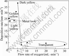
Fig.1 Deposition rate of TiO2 films as function of flow rate of oxygen
3.2 Surface morphology
AFM images of the films are presented in Fig.2. All samples are similarly composed of close nanoparticles with size ranging from 10 to 100 nm. The films deposited at oxygen flow rate of 10, 20, 30 mL/min exhibit smaller and more uniform particles than that of 7 mL/min. The Rrms is the most widely used parameter to characterize film surface roughness, which can be
expressed as ![]() , where Zi is
, where Zi is
measured height of i-th point in the scan area, ![]() is the average of height and N is the number of all points defined in scanned area. The film deposited at 10 mL/min exhibits the lowest Rrms, about 3.64 nm, while the film at 7 mL/min is the highest, with a Rrms of 4.60 nm. The film deposited at oxygen flow rate of 20 mL/min exhibits the biggest particles, with a Rmax of about 44.23 nm. The deposition rate increases with the oxygen flow rate from 0 to 5 mL/min and thereafter decreases. Due to the different deposition models (see Fig.1), the deposition rate in metallic model is greater than that of oxide model, some adsorption atoms fail to have enough time to migrate to the sites where the surface energy is the lowest, and then are covered by the coming atoms. The film surface is very rough. As the oxygen flow rate further increases, the films become transparent. Maybe because of the unstable sputtering, which suddenly shifts in deposition model, the film deposited at 7 mL/min is rougher than other transparent films.
is the average of height and N is the number of all points defined in scanned area. The film deposited at 10 mL/min exhibits the lowest Rrms, about 3.64 nm, while the film at 7 mL/min is the highest, with a Rrms of 4.60 nm. The film deposited at oxygen flow rate of 20 mL/min exhibits the biggest particles, with a Rmax of about 44.23 nm. The deposition rate increases with the oxygen flow rate from 0 to 5 mL/min and thereafter decreases. Due to the different deposition models (see Fig.1), the deposition rate in metallic model is greater than that of oxide model, some adsorption atoms fail to have enough time to migrate to the sites where the surface energy is the lowest, and then are covered by the coming atoms. The film surface is very rough. As the oxygen flow rate further increases, the films become transparent. Maybe because of the unstable sputtering, which suddenly shifts in deposition model, the film deposited at 7 mL/min is rougher than other transparent films.
3.3 Phase structure
Fig.3 shows the XRD patterns of the TiO2 films.
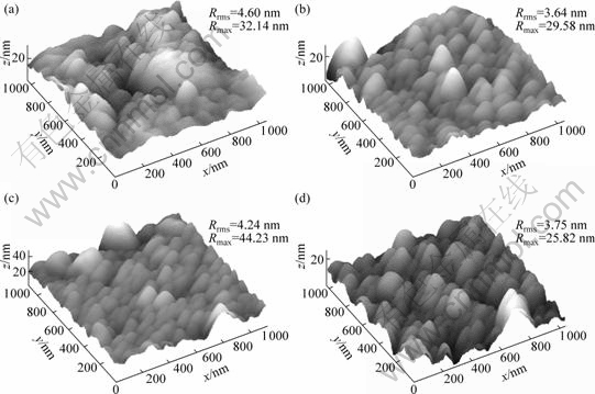
Fig.2 AFM images for sample prepared at oxygen flow rate of 7 mL/min (a), 10 mL/min (b), 20 mL/min (c) and 30 mL/min (d)
The films deposited at oxygen flow rate of 3 and 30 mL/min have only one broad scattering peak occurring at 25? from the glass substrate. The films deposited at oxygen flow rate of 3 mL/min also show broad features at 44? and 64? from TiOx (x<2). Generally, TiO2 is found in two stable crystalline phases, anatase and rutile[16]. Only anatase and rutile have been observed in thin films prepared by reactive magnetron sputtering up to now[17]. It is concluded that a crystalline anatase phase is present, possibly mixed with an amorphous phase, in the films deposited at oxygen flowrate of 7, 10 and 20 mL/min. It is worth noting that, oxygen plays an important role in
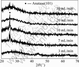
Fig.3 XRD patterns of TiO2 films deposited at different oxygen flowrate
the crystallization of TiO2 films.
The grain size of the TiO2 thin films increases as the oxygen flow rate increases from 3 to 10 mL/min, and decreases as the oxygen flow rate increases from 10 to 30 mL/min. Inadequate or excessive oxygen makes the film difficultly crystallize. That is because oxygen atoms are reflected from the target and hit the substrate with appreciable energy, thereby causing nucleation. However, too much oxygen will decrease the presence of Ti atoms in the vapor phase, thereby hindering nucleation. Similar phenomenon was observed by DANNENBERG and GREENE[18], that the films were polycrystalline at higher oxygen flow rate, however became amorphous near the turning point. They did not find that too much oxygen also make the film become amorphous.
3.4 Optical properties
Fig.4 shows the transmission spectra of TiO2 thin films deposited at different oxygen flowrate. As the oxygen flow rate increases from 7 to 10 mL/min, the absorption edge shifts from 353 to 356 nm. When the oxygen flow rate increases from 20 to 30 mL/min, the absorption edge shifts from 367 to 353 nm. The fluctuation arises from the change of the grain size. This result differs from ZHANG et al[19], who thought this blue shift was arisen from particle size. In Ref.[19], the absorption edge shifted to shorter wavelength as particle size decrease obtained from AFM. The film was amorphous, which was deduced from XRD, however, it was not confirmed by other analysis such as transmission electron microscopic (TEM). AFM can only estimate the particle size; however, XRD can estimate the grain size. One or more grains can exist in the same particle. In this work, the shift tendency of absorption edge does not strictly agree with the change of particle size obtained from AFM, however, consists with the change of crystal grain size got from XRD. So, the absorption edge may be directly related with crystal grain size.
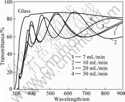
Fig.4 Transmission spectra of TiO2 thin films deposited at different oxygen flowrate
The transmittance spectra show that all the films, deposited in oxide mode are transparent in the visible light region and their spectra exhibit a sharp decrease in the UV region because of the fundamental light absorption. The oscillation in these spectra is connected with the film thickness and consequently with the constructive and destructive interference caused by the difference in refractive index between the film and the substrate. All the films deposited in this work have the same thickness. Therefore, the difference of oscillation is thought to be connected with interference. The film at oxygen flow rate of 10 mL/min with a lower roughness shows higher transmittance with higher interference oscillation. Similar phenomenon was observed by others[20]. Film surface roughness and thickness inhomogeneity have a large influence on the optical transmission spectrum, which mainly occurs in transparent zone and weak-absorption zone. The increase of the surface roughness leads to the decrease of the peak values and the distorted vibration period[21]. The transmittance spectrum of the film at oxygen flow rate of 10 mL/min has three peaks and larger peak values. This may be the reason that the film at oxygen flow rate of 10 mL/min has a better transmittance.
Fig.5 shows the linearity of the direct band gap Tauc fits. Because the films have small crystal grains, we assume a direct transition between the top of the valence band and the bottom of the conduction band. The optical band gap (Eg) of the films is estimated by using the relation[22] of (��h��)2=A(h��-Eg), where h�� is the photon energy, Eg is the optical band gap and A is a constant which does not depend on the photon energy. The optical band gap of film is determined from the extrapolation of the linear plots of (��h��)2 versus h�� at ��=0. �� is the absorption coefficient and calculated by ln(1/T)/d, where T is the transmission coefficient and d is the film thickness. The Eg values of the TiO2 films at oxygen flow rate of 7, 10, 20, and 30 mL/min are 3.38, 3.46 and 3.42 eV, respectively, which is in good agreement with both direct and indirect gaps reported in Ref.[15]. It can be seen from Fig.5, the optical band gap becomes larger as the oxygen flow rate increases. This trend does not include the film at oxygen flow rate of 30 mL/min. Because the film at 30 mL/min is amorphous, it is assumed as indirect band gap.
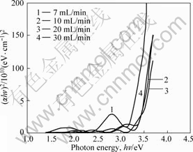
Fig.5 (��h��)2 versus photon energy plot of TiO2 films deposited at different oxygen flowrate
Fig.6 shows the dependence of average transmittance and grain size of the film on oxygen flow rate. The crystallite size is estimated from the Debye�C Scherrer��s equation using the XRD line broadening as follows: D=0.94��/(��cos��), where D is the crystallite size, �� is the wavelength of the X-ray radiation (��=0.154 06 nm), �� is the diffraction angle and �� is the full width at half maximum height. It can be seen that the film at oxygen flow rate of 10 mL/min has a larger transmittance and a lower surface roughness. The film deposited at oxygen flow rate of 20 mL/min, which is better than the film at oxygen flow rate of 7 mL/min in surface roughness, has a worse transmittance, because the film deposited at oxygen flow rate 20 mL/min has a larger grain size than others. Grain boundaries in polycrystalline films cause scattering and decrease transparency. The film at oxygen flow rate of 30 mL/min is amorphous and the surface roughness is better than the film at oxygen flow rate of 7 mL/min, however, the film at oxygen flow rate of 30 mL/min is also worse than the film at oxygen flow rate of 7 mL/min in transparency. This means the amorphous materials are not suitable for fabricating AR coating, because of the absorption of the unsaturated bonds in amorphous materials. Therefore, the desirable TiO2 AR coating should be of smooth surface and nano-crystalline.
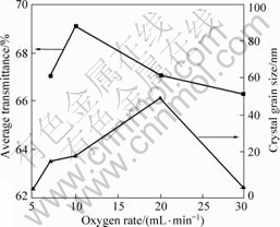
Fig.6 Dependence of average transmittance and grain size of TiO2 film on oxygen flow rate
4 Conclusions
1) By reactive magnetron sputtering, the TiO2 films were prepared on glass substrates. The oxygen flow rate has an important influence on the structural, morphological and optical properties of the TiO2 thin films. The deposition mode is in metallic mode when the oxygen flow rate is less than 7 mL/min, and in oxide mode when the oxygen is larger than 7 mL/min. The thin film prepared at 7 mL/min has the minimum optical band of 3.38 eV.
2) While deposited at the oxygen flow rate of 7-20 mL/min, the TiO2 thin film is nanocrystalline; otherwise, the TiO2 thin film is amorphous. Under our experimental conditions, the TiO2 thin films deposited at 10 mL/min has the lowest roughness, the suitable grain size and the highest average transmittance.
3) The absorption edge of the TiO2 thin films shifts to longer wavelengths as the oxygen flow rate increases from 7 to 10 mL/min, and shifts to shorter wavelengths as the oxygen flow rate increases from 10 to 30 mL/min. This tendency is arisen from the change of crystal grain size.
References
[1] CAMPBELL P, GREEN M A. Light trapping properties of pyramidally textured surfaces [J]. J Appl Phys, 1987, 62: 243-249.
[2] LO S S, CHEN C C, GARWE F, PERTCH T. Broad-band anti- reflection coupler for a: Si thin-film solar cell [J]. J Phys D: Appl Phys, 2007, 40: 754-758.
[3] RICHARDS B S. Comparison of TiO2 and other dielectric coatings for buried-contact solar cells: A review [J]. Prog Photovolt: Res Appl, 2004, 12(4): 253-281.
[4] RICHARDS B S, ROWLANDS S F, UERANATASUN A, COTTER J E, HONSBERG C B. Potential cost reduction of buried-contact solar cells through the use of titanium dioxide thin films [J]. Sol Energy, 2004, 76: 269-276.
[5] ZRIBI M, KANZARI M, REZIG B. Structural, morphological and optical properties of thermal annealed TiO thin films [J]. Thin Solid Films, 2008, 516: 1476-1479.
[6] WANG W H, CHAO S. Annealing effect on ion-beam-sputtered titanium dioxide film [J]. Optics Letters, 1998, 23(18): 1417-1419.
[7] TAVARES C, VIEIRA J, REBOUTA L, HUNGERFORD G, COUTINHO P, TEIXEIRA V, CARNERIO J O, FERNADES A J. Reactive sputtering deposition of photocatalytic TiO2 thin films on glass substrates [J]. Mat Sci Eng B, 2007, 138(2): 139-143.
[8] FRENCK H J, KULISCH W, KUHR M, KASSING R. Deposition of TiO2 thin films by plasma-enhanced decomposition of tetraisopropyltitanate [J]. Thin Solid Films, 1991, 201(2): 327-355.
[9] CHOI J W, LEE S E, LEE B G, JEONG Y S, OH H J, CHI C S. Purifying behavior of photocatalytic TiO2 anodized in nitrate ion containing solution [J]. Trans Nonferrous Met Soc China, 2009, 19(4): 1027-1030.
[10] KUBO Y, IWABUCHI Y, YOSHIKAWA M, SATO Y, SHIGESATO Y. High rate deposition of photocatalytic TiO2 films with high activity by hollow cathode gas-rate sputtering method [J]. J Vac Sci Technol A, 2008, 26(4): 893-897.
[11] VALE A, CHAURE N, SIMONDS M, RAY A, BRICKLEBANK N. Sputtered rutile stoichiometric TiO2 nanocrystalline films [J]. J Mater Sci: Mater Electron, 2006, 17(10): 851-855.
[12] ZHOU J C, luo d t, li y z, liu z, Effect of sputtering pressure and rapid thermal annealing on optical properties of Ta2O5 thin films [J]. The Chinese Journal of Nonferrous Metals, 2009, 19(2): 359-363. (in Chinese)
[13] LAPOSTOLLE F, BILLARD A, von STEBUT J. Structure/ mechanical properties relationship of titanium-oxygen coatings reactively sputter-deposited [J]. Surf Coat Technol, 2000, 135(1): 1-7.
[14] MARTIN N, SANTO A M E, SANJIN?S R, L?VY F N. Energy distribution of ions bombarding TiO2 thin films during sputter deposition [J]. Surf Coat Technol, 2001, 138(1): 77-83.
[15] LI Z G, MIYAKE S, MAKINO M, WU X Y. Metallic sputtering growth of crystalline titanium oxide films on unheated glass substrate using inductively coupled plasma assisted direct current magnetron sputtering [J]. Thin Solid Films, 2008, 517: 699-703.
[16] HOSSAIN M F, BISWAS S, TAKAHASHI T, KUBOTA Y, FUJISHIMA A. Influence of direct current power on the photocatalytic activity of facing target sputtered TiO2 thin films [J]. Thin Solid Films, 2008, 517: 1091-1095.
[17] L?BL P, HUPPERTZ M, MERGEL D. Nucleation and growth in TiO2 films prepared by sputtering and evaporation [J]. Thin Solid Films, 1994, 251: 72-79.
[18] DANNENBERG R, GREENE P. Reactive sputter deposition of titanium dioxide [J]. Thin Solid Films, 2000, 360: 122-127.
[19] ZHANG M, LIN G Q, DONG C, WEN L S. Amorphous TiO2 films with high refractive index deposited by pulsed bias arc ion plating [J]. Surf Coat Technol, 2007, 201: 7252-7258.
[20] TIGAU N. Substrate temperature effect on the optical properties of amorphous Sb2S3 thin films [J]. Cryst Res Technol, 2006, 41(5): 474�C480.
[21] YU Yun-peng, LIN Shun-hui,; HUANG Chong, LIN Xuan-ying. Effect of thickness homogeneity on optical transmittance spectra of a-Si: H films [J]. J Shantou Univ (Nat Sci), 2004, 19(1):50-54. (in Chinese)
[22] HEMISSI M, AMARDJIS-ADNANJ H, PLENET J C. Titanium oxide thin layers deposed by dip-coating method: Their optical and structural properties [J]. Current Applied Physics, 2009, 9: 717-721.
Foundation item: Project(08FJ1002) supported by the Hunan Province Key Project of Science and Technology, China
Corresponding author: ZHOU Ji-cheng; Tel: +86-13873193957; E-mail: jicheng@mail.csu.edu.cn
DOI: 10.1016/S1003-6326(09)60316-2
