

Correlations between IMC thickness and three factors in Sn-3Ag-0.5Cu alloy system
MENG Gong-ge(�Ϲ���)1, T. Takemoto2, H. Nishikawa2
1. College of Materials Science and Engineering, Harbin University of Science and Technology,Harbin 150040, China;
2. Joining and Welding Research Institute, Osaka University, Ibalaki, Osaka 567-0047, Japan
Received 15 January 2007; accepted 28 May 2007
Abstract:
The effects of Ni content, soldering temperature and time on the IMC thickness in Sn-3Ag-0.5Cu and Sn-3Ag-0.5Cu-0.2Co alloys were researched using uniform design method and computer programs. For each alloy, the factors were divided into three levels in the experiment. Two correlative equations are given by regression. They indicate that the effects of three factors on the function are in the mutual and quadratic forms. And the analysis of variance shows the equations are sound and meaningful. Using the equations, it is easy to search, predict and control the IMC thickness. The existence of element Co accelerates the crystallization and growing up of IMC.
Key words:
lead-free solder; Sn-Ag-Cu alloy; IMC thickness; uniform design;
1 Introduction
Due to environmental concerns over lead containing solders, the electronic industry has been actively searching for lead free solders for nearly two decades. The European legislation has become effective on July 1, 2006, and almost all Japanese major electric and electronic manufacturing companies will finish their development of lead free soldering [1].
To replace the traditional solder Sn-Pb alloys, the lead-free systems have been developed. Among the various alloy systems being considered as lead-free solder candidates, Sn-Ag-Cu alloys have been recognized as the most promising material because of their excellent reliability and compatibility with current components, many of which have Sn-Pb surface finish [2-4].
Generally speaking, lead free solders desire many characteristics, namely, adequate melting point, wetting or spreading behavior and many merits of physical, mechanical properties. But very different from the traditional Sn-Pb alloys, the lead-free systems always form intermetallic compounds(IMCs). Sometimes the IMCs improve the mechanical, fatigue and creep properties. But they have a brittle nature, so they have drawbacks especially growing thick at the solder/ substrate interface[5-7].
IMCs formed both at the solder/substrate interface and within the solder during reflow exhibit different morphological features and mechanical properties depending on the conditions employed. The thickness of the IMC layer depends on a number of factors, such as temperature, time, volume of solder, property of the solder alloy and morphology of the deposit. Many investigators have studied the intermetallic formation in the liquid solder/solid substrate interface [8-11]. And intermetallic growth rate for solid-liquid couples is significantly faster compared with growth rate for solid-solid couples. In some papers the intermetallic compound growth in the Sn-Ag-Cu lead-free solder and on the joint has been studied [12-14].
Based on uniform design thought, method and computer software [15], the practical correlation between IMC thickness and three factors was searched in this study. The experimental points were arranged according to this method and software, and the data was dealt with it too. By this method, it can be judged that if the correlation exist and can give quantitatively the influenced pattern and degree of the factors on the thick-
Corresponding author: MENG Gong-ge; Tel: +86-451-82735289; E-mail: menggongge@yahoo.com, menggongge@hrbust.edu.cn
ness. The alloys selected are Sn-3Ag-0.5Cu (abbreviated as 0Co) and Sn-3Ag-0.5Cu-0.2Co (abbreviated as 0.2Co).
2 Experimental
In the experiment, the solder composition (Ni content), soldering temperature and soldering time are taken as three factors, that is, three variables, and the IMC thickness as function. Tables 1 and 2 give the design plan and the experimental point distribution by uniform design computer program. And each factor is divided into three levels. The Ni and Co contents are in the nominal chemical composition.
Table 1 Experimental point distribution and thickness measuring result according to uniform design (0Co)
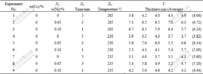
Table 2 Experimental point distribution and thickness measuring result according to uniform design (0.2Co)
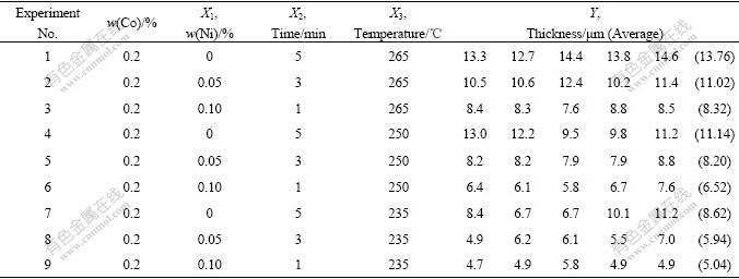
0, 0.05% and 0.1% Ni were put into Sn-3Ag-0.5Cu solder alloy or Sn-3Ag-0.5Cu-0.2Co solder alloy separately. These alloys were obtained from commercial company according to the nominal chemical composition in Tables 1 and 2 in the form of solid wire. The size of Cu plates are 30 mm��30 mm��0.3 mm. The soldering was done in a box furnace (SMT Scope SA-5000 D1).
Before soldering, the Cu plates were rinsed in hydrochloric acid ethanol solution and cleaned with ethanol. The solder wire was cut for 0.3 g and circled. After cleaning with ethanol, put it on the Cu plate and add RMA flux. The soldering process was protected using nitrogen air with flowing rate of 2 L/min. The heating profile model is shown in Fig.1. The final temperature and time are different for every specimen according to Tables 1 and 2.
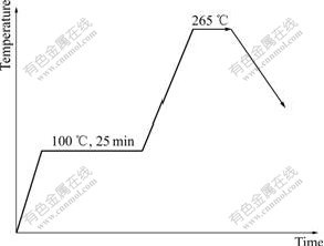
Fig.1 Heating temperature and keeping time profile for soldering
After soldering, the specimens were cleaned with ethanol in the ultrasonic box and blown dry. Then the specimens were cut and mounted in an epoxy-molding compound. When polishing was finished, the final IMC thickness measurement was done with digital optical electronic microscope (KEYENCE VH-7000).
3 Results and discussion
3.1 IMC thickness measurement, regressive figures and quotations
The thickness measuring results are shown in the Tables 1 and 2. The optical morphologies of thickness measuring examples are shown in Fig.2. And for every specimen the measurement has been conducted 5 times. Then put the data of Tables 1 and 2 into computer, Figs.3-5 and the equations are regressed out using uniform design and data processing program.
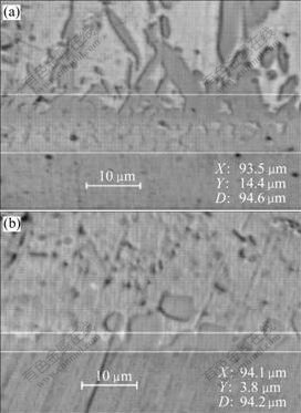
Fig.2 Optical images of thickness measuring examples: (a) 0.2Co-0Ni, 265 ��, 5 min; (b) 0Ni, 265 ��, 5 min
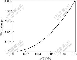
Fig.3 Relationship between Ni content and IMC thickness (0.2Co)
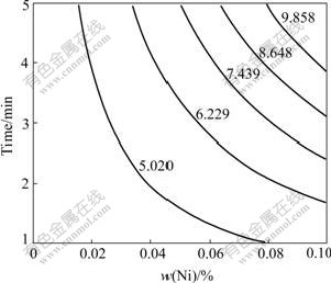
Fig.4 Isograms of IMC thickness (0Co)
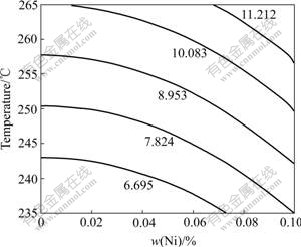
Fig.5 Isograms of IMC thickness (0.2Co)
Fig.3 shows the relationship between Ni content and IMC thickness (0.2Co). It shows the quadratic/parabolic curve feature. Figs.4 and 5 show the isograms of IMC thickness for 0Co and 0.2Co. The former is from Ni content and time, the later from Ni content and temperature. And it is apparent that the IMC thickness increases as the Ni content, soldering temperature and time increase.
Two equations give the correlations between the IMC thickness and three factors (Ni content, time and temperature above solder liquidus during the soldering). Eqn.(1) indicates that Ni content and soldering time have pronounced mutual effect on the function, and elevated temperature has quadratic effect. Eqn.(2) shows that Ni content and elevated temperature has significant quadratic effect separately, while elevated temperature and time have mutual effect:
Y(0Co)=-1.452 42+1.453 33��10X1X2+8.405 03��10-5X3X3 (1)
Y(0.2Co)=-1.360 20��10+2.299 70��102X1X1+6.866 89��10-3X2X3+2.586 39��10-4X3X3 (2)
Moreover, it is clear that the two equations are different though the three factors do have effects on the function. They indicate that the effects of factors on the function are not always individual, linear and simple, and the most forms are mutual, quadratic and complex.
3.2 Reliability of regressive equations
The analyses of variance with mathematical statistics to validate Eqns.(1) and (2) are listed in Tables 3 and 4.
Table 3 Analysis of variance on regressive equation (0Co)
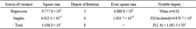
Table 4 Analysis of variance on regressive equation (0.2Co)
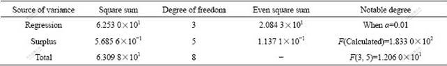
The results of analysis of variance mean that the two equations are true and notable. Figs.6 and 7 give the results of test and calculation. It is apparent that the results of test and calculation are consistent.
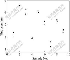
Fig.6 Data (0Co) by test (circle) and calculation (square)
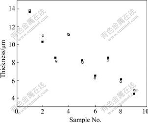
Fig.7 Data (0.2Co) by test (circle) and calculation (square)
3.3 Searching and predicting
With uniform design and regressive analysis program, the searching, optimizing and predicting can be done. For example, the minimum and maximum IMC thickness is 3.6, 6.72 ��m (0Co) and 5.04, 13.76 ��m (0.2Co) respectively in the experiment. It is searched, optimized and predicted as 3.18, 11.717 ��m under the condition of X1=0, X2=1, X3=235 and X1=0.1, X2=5, X3=265 (0Co). It is searched, optimized and predicted as 2.312, 15.980 ��m under the condition of X1=0, X2=1, X3=235 and X1=0.1, X2=5, X3=265 (0.2Co). So it is easy to control the IMC thickness by changing conditions.
By comparing Table 1 and Table 2, it is clear that the existence of element Co accelerates the crystallization and growing up of IMC. The mechanism will be discussed later.
4 Conclusions
1) Two correlative equations are given by regression. They indicate that the effects of Ni content, soldering temperature and time on the IMC thickness in Sn-3Ag- 0.5Cu and Sn-3Ag-0.5Cu-0.2Co alloys are in the mutual and quadratic forms.
2) The analysis of variance with mathematical statistics shows that the two equations are sound and meaningful.
3) Using the two equations and computer program, it is easy to search, predict and control the IMC thickness in this alloy systems or control the IMC thickness by adjusting the parameter.
4) The existence of element Co accelerates the crystallization and growing up of IMC.
References
[1] TAKEMOTO T. Introduction of JIS related to lead-free solder and soldering [C]// WANG Chun-qing. 6th International Conference on Electronics Packaging Technology: ICEPT2005 Proceedings. Shenzhen: IEEE China Electronic Packaging Society, 2005: 8-12.
[2] TU K N, GUSAK A M, LI M. Physics and materials challenges for lead-free solders [J]. Journal of Applied Physics, 2003, 93: 1335-1353.
[3] ZENG K, TU K N. Six cases of reliability study of Pb-free solder joints in electronic packaging technology [J]. Materials Science and Engineering R, 2002, 38: 55-105.
[4] KIM K S, HUH S H, SUGANUMA K. Effects of fourth alloying additive on microstructures and tensile properties of Sn-Ag-Cu alloy and joints with Cu [J]. Microelectronics Reliability, 2003, 43: 259-267.
[5] XIE Hai-ping, YU Da-quan, MA Hai-tao, WANG Lai. Microstructure, wettability and mechanical properties of Sn-Zn-Cu lead free solder [J]. The Chinese Journal of Nonferrous Metals, 2004, 14: 1694-1699. (in Chinese)
[6] WU Pei-lin, HUANG Meng-kuang, LEE Chiapyng, TZAN Shyh-rong. Effects of different printed-circuit-board surface finishes on the formation and growth of intermetallics at thermomechanically fatigued, small outline J Leads/Sn-Ag-Cu interfaces [J]. Journal of Electronic Materials, 2004, 33: 157-161.
[7] HE Da-peng, YU Da-quan, WANG Lai, WU C M L. Effect of Cu content on IMC between Sn-Cu solder and Cu and Ni substrates [J]. The Chinese Journal of Nonferrous Metals, 2006, 16: 701-708. (in Chinese)
[8] LEE J G,CHEN K C,SUBRAMANIAN K N. Formation and growth of intermetallics around metallic particles in eutectic Sn-Ag solder [J]. Journal of Electronic Materials, 2003, 32: 1240-1248.
[9] SHARIF A,CHAN Y C. Comparative study of interfacial reactions of Sn-Ag-Cu and Sn-Ag solders on Cu pads during reflow soldering [J]. Journal of Electronic Materials, 2005, 34: 46-52.
[10] ANDERSON I E,FOLEY J C,COOK B A, HARRINGA J, TERPSTRA R L, UNAL O. Alloying effects in near-eutectic Sn-Ag-Cu solder alloys for improved microstructural stability [J]. Journal of Electronic Materials, 2001, 30: 1050-1059.
[11] ABTEW M, SELVADURAY G. Lead-free solders in microelectronics [J]. Materials Science and Engineering R, 2000, 27: 95-141.
[12] LEHMAN L P, ATHAVALE S N, FULLEM T Z, GIAMIS A C, KINYANJUI R K, LOWENSTEIN M, MATHER K, PATEL R, RAE D, WANG J, XING Y, ZAVALIJ L, BORGESEN P, COTTS E J. Growth of Sn and intermetallic compounds in Sn-Ag-Cu solder [J]. Journal of Electronic Materials, 2004, 33: 1429-1439.
[13] PANG J H L, XU Lu-hua, SHI X Q, ZHOU W, NGOH S L. Intermetallic growth studies on Sn-Ag-Cu lead-free solder joints [J]. Journal of Electronic Materials, 2004, 33: 1219-1226.
[14] LI De-zhi, LIU Chang-qing, CONWAY P P. Characteristics of intermetallics and micromechanical properties during thermal ageing of Sn-Ag-Cu flip-chip solder interconnects [J]. Materials Science and Engineering A, 2005, 39: 95-103.
[15] ZHANG Cheng-en. Uniform design and parameter optimization [EB/OL]. http://xyzok.126.com/, 2006-11-09.
