
Trans. Nonferrous Met. Soc. China 22(2012) s740-s744
Effect of substrate bias on microstructure and tribological performance of GLC films using hybrid HIPIMS technique
ZHANG Xue-qian1, 2, KE Pei-ling1, WANG Ai-ying1, HUANG Mei-dong2, Kwang Ho KIM3
1. Ningbo Key Laboratory of Marine Protection Materials, Ningbo Institute of Materials Technology and Engineering, Chinese Academy of Sciences, Ningbo 315201, China;
2. College of Physics and Electronic Information, Tianjin Normal University, Tianjin 300387, China;
3. National Core Research Center for Hybrid Materials Solution��Pusan National University, Busan 609-735, Korea
Received 21 May 2012; accepted 2 November 2012
Abstract:
The Cr-doped hydrogen-GLC films were prepared by a hybrid magnetron sputtering system composed of a direct current magnetron sputtering (DC-MS) source of carbon and a high power impulse magnetron sputtering (HIPIMS) source of Cr with reactive gas of C2H2. The hydrogen-free GLC and Cr-doped GLC films were also prepared for comparison. The influence of substrate bias on the Cr-doped hydrogen-GLC films was investigated. With the increase of substrate bias from -100 V to -250 V, the re-sputtering of weak bonding sp2 firstly occurred and induced an increased sp3 bonding. However, the following sp3 to sp2 transformation resulted in a decreased sp3 bonding. The change trends of surface roughness and friction coefficient with the increased bias voltages were the same as those of sp3 bond. The lowest surface roughness and lowest friction coefficient corresponded to the highest sp3 with the Cr-GLC-H films at the bias voltage of -100 V.
Key words:
graphite-like carbon; high power impulse magnetron sputtering; substrate bias; microstructure; tribological behavior;
1 Introduction
Carbon is one of the most remarkable elements among all others in the periodic table. It has the largest number of allotropes and can exist in many forms ranging from diamond and graphite (3D) to graphene (2D) [1], nanotubes (1D) [2] or fullerenes (0D) [3]. With the exception of diamond, it is possible to think of fullerenes, nanotubes and graphite as different structures built from the same hexagonal array of sp2 carbon atoms which were reported to possess exceptional mechanical properties. As for thin film field, amorphous graphite like carbon (GLC) films with highly sp2 bond structure were reported to demonstrate an excellent wear resistance and high load-bearing capacity meanwhile remaining a relatively high hardness. These properties make GLC an ideal coating for high-load wear applications and cutting tools especially for difficult machine materials.
Nowadays, amorphous GLC thin films are possible to be fabricated by using numerous techniques including ion beam sputtering, magnetron sputtering, laser ablation and vacuum cathodic arc. All these techniques in common are aimed to generate an intense bombardment of energetic ions to control the formation of sp2/sp3 bond during the film growth. Therefore, it is of fundamental importance to understand the effect of substrate bias on the formed film structure especially sp3/sp2 ratio.
One of the main problems for the further application of GLC films is the poor adhesion to different substrates. Previous studies showed that the adhesion and toughness in the films can be markedly increased by buffer layer and interlayer [4]. Magnetron sputtering, the traditional method to produce a buffer layer and interlayer, is a technique of neutral atom deposition, only a few of the sputtered atoms are ionized, so the adhesion is weak. High power impulse magnetron sputtering (HIPIMS) is an important physical vapor deposition (PVD) process in which the power density exceeds conventional power density by about three orders of magnitude. Electrostatic probe measurements show that plasma density of about 1019 m-3 can be generated [5,6]. The fraction of ionized sputtered copper can approach to 70% [7]. Therefore, HIPIMS can provide a highly ionized flux of sputtered species, and thus a promising technique to prepare a buffer layer with good adhesion strength [7-10].
In this work, a hybrid system was used, which is composed of a direct current magnetron sputtering (dc-MS) source of carbon and a high power impulse magnetron sputtering (HIPIMS) source of Cr with reactive gas of C2H2. The hydrogen-free GLC, Cr-doped GLC films (Cr-GLC) and the Cr-doped hydrogen-GLC films (Cr-GLC-H) were prepared for comparison. The influence of substrate bias on the Cr-GLC-H films was investigated to study the formed film structure and its tribological behaviors.
2 Experimental
High speed steel (HSS) and silicon (100) wafers were used as the substrate materials. All the substrates were cleaned ultrasonically in acetone and ethanol, and dried in air before being putted into the vacuum chamber. The films were prepared on the HSS and silicon substrates by a HIPIMS with a 120 mm��380 mm rectangular Cr target (99.99%) and DC magnetron sputtering with a 120 mm��380 mm rectangular C target (99.99%). Prior to deposition, the substrates were cleaned with Ar plasma sputtering at a bias voltage of 500 V for 20 min so as to remove the native oxide on the substrates. The base pressure was evacuated to a vacuum of 4��10-3 Pa.
In the preparation process, the HIPIMS with Cr target was used to prepare the Cr buffer layer with Ar as sputtering gas. Next, the HIPIMS with Cr target was used to prepare the CrC inter-layer with Ar as sputtering gas and C2H2 as reactive gas. Last, the DC magnetron sputtering source with a C target was used to prepare the GLC with Ar as sputtering gas. Cr doping was achieved by HIPIMS and C2H2 gas was introduced to form hydrogen containing films. Different negative bias voltages were applied to substrate for Cr-GLC-H films.
Raman spectroscopy with an incident Ar+ beam at a wavelength of 514.5 nm was used to measure the atomic bonds of films. An X-ray photoelectron spectroscopy (XPS) with Al K�� irradiation at pass energy of 160 eV was used to characterize the chemical bonds and microstructure of the films. The thickness of the deposited films was measured by a step profiler. The tribological behaviors of the treated sample were investigated on a rotary ball-on-disk tribometer at room temperature under dry sliding conditions. Bearing steel with a diameter of 6 mm was used as the friction counter body. All the tests were performed at a sliding speed of 100 mm/s and the applied load was 3 N. An MTS nano-indenter was performed to test the hardness and elastic modulus of the treated samples in this study.
3 Results and discussion
3.1 Chemical bonds structure of GLC films
The chemical bonds of the deposited films can be observed from the XPS spectra. Figure 1 shows the XPS C1s peaks of the pure GLC, Cr-GLC and Cr-GLC-H films. The final peak shape should be Lorentzian and Gaussian convolution of the Voigt peak shape obtained [11,12]. Fitted variables included sp2 peak energy, sp3 and sp2 peak energy difference, and C��O and C=O peak energy of small fluctuations. These were the single C��O bond at 286.6 eV, the double C=O bond at 287.7 eV, the sp2 bond at 284.6 eV, the sp3 bond at 285.4 eV and Cr��C bond at 283 eV (Cr7C3 at 283.1 eV, Cr3C2 at 282.94 eV, Cr2C3 at 282.8 eV etc.) [13]. The integration results are listed in Table 1, the sp2 contents of the three GLC films are more than 65%. The content of sp2 bond in GLC film increases when metal Cr is doped. And a small content of chromium carbide crystalline phase was detected in the amorphous carbon matrix of the film. As for Cr-GLC-H films, a slight decrease of sp2 content is due to the fact that, C2H2 decomposes into carbon and hydrogen and forms C��H sp3 bonds.
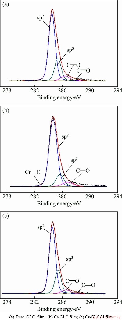
Fig. 1 XPS C1s spectra of GLC films
Table 1 Bonding contents in GLC films
Raman spectroscopy is a fast and nondestructive tool for characterization of amorphous carbons. All amorphous carbon show the common features in Raman spectra in the region of 800-2000 cm-1, the so-called peaks G and D, which lie at around 1560 cm-1 and 1360 cm-1. The peak G is due to the bond stretching of all pairs of sp2 atoms in both rings and chains. The peak D is due to the breathing modes of sp2 atoms in rings [14,15]. As shown in Fig. 2, according to the intensity ratio of peak D to peak G (ID/IG), the sp2/sp3 ratio of the amorphous carbons films can be characterized [14]. As the sp2/sp3 ratio decreases in hydrogenated amorphous carbon, the ID/IG ratio will decrease. By integrating, the ID/IG is 1.578, 1.790 and 1.242 for GLC, Cr-GLC and Cr-GLC-H films, respectively. The ratio increases in the Cr-GLC film, implying that the sp2/sp3 ratio in the Cr-GLC films is higher than that in the GLC film. The increase of the sp2/sp3 ratio due to Cr doping might attribute to the catalyst effect of atoms on the formation of sp2 sites. It is found that the Cr-GLC-H films show strong photoluminescence background (PL) in visible Raman spectroscopy due to the hydrogen saturation of the non-radiative recombination centers, which notes H element in the film[16]. The ratio decreased in the Cr-GLC-H films, implying that the sp2/sp3 ratio in the Cr-GLC-H films is lower that that in the Cr-GLC. The hydrogen is expected to correlate with sp3 fraction site, because the hydrogen preferable saturates the C=C sp2 bonds and promotes the transformation from sp2 sites to sp3 sites [17]. This is consistent with the XPS result.
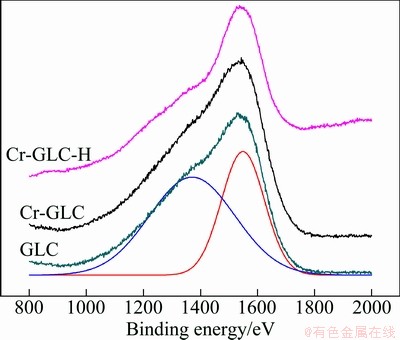
Fig. 2 Raman spectra with different types of GLC films
3.2 Effect of substrate bias on microstructure of GLC films
Table 2 displays XPS results of the chemical bond composition with applied bias voltages. At -100 V bias voltage, the chromium content is near zero which might be caused by the ��target poisoning�� due to the interaction of the target with the C2H2. With a higher bias voltage, the phenomenon disappears. The chromium content is increased with an increasing bias voltage, during which more Cr ions are attracted towards the substrate. The oxygen in the films is due to O2 within the vacuum chamber and films reacted with the O2.
Table 2 Cr-GLC-H films composition with different bias voltages
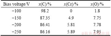
Figure 3 presents the C1s and Cr2p XPS spectra of Cr-GLC-H films with different applied bias voltages. As the bias voltage is -100 V, the Cr2p has no peak which is due to target poisoning. When the voltage is higher than -100 V, the Cr2p shows a major peak at a binding energy around 574 eV and a shoulder around 583.7 eV. Actually, it is difficult to identify the chromium carbide in Cr2p. The C1s peak is combined to determine the chromium carbide. There is no peak around 283 eV, which means the metal chromium atoms distributing in the Cr-GLC-H films. The relative intensity of C1s peak has a maximum value at -100 V, which again verifies the occurrence of target poisoning and causes a low content of carbon.
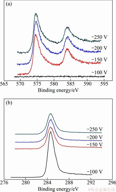
Fig. 3 Cr2p and C1s XPS spectra of Cr-GLC-H films with different bias voltages
The integration sp2 bond at 284.6 eV and sp3 bond at 285.4 eV are shown in Fig. 4. The sp2 content is firstly decreased and then increases, and the sp3 content is just the reverse. This variation trend consists of a chemical adsorption process of the species on the growing surface and a physical process of implantation at the subsurface, which mainly depends on the ion energy. At a low bias voltage, the ion energy is too weak to penetrate into the growing surface and most of the ions are trapped on the growing surface, resulting in the formation of the sp2 bond. Increasing the negative bias voltage to -150 V, the ion species will have sufficient energy (80-100 eV per atom) to penetrate into the subsurface. Under this condition, the sp2 bond turns to the sp3 bond. However, at higher bias voltage more than -150 V, the dissipation of the excess heat generated by impinging the energetic ions can relax the high compressive stress that leads to loose carbon networks, which leads to the sp3 to sp2 bonds transformation.
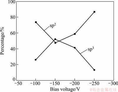
Fig. 4 C bonding percentage with different bias voltages
AFM images shown in Fig. 5 illustrate the effect of the bias voltage on the Cr-GLC-H surface roughness and feature. With the bias voltage at the range from -100 V to -250 V, the surface roughness in turn is 2.52, 3.78, 3.50, 3.08 nm, respectively. The films deposited at all applied bias voltages show very smooth and flat surfaces, which are benefited from this hybrid HIPIMS technique. The surface of the Cr-GLC-H films is the smoothest at bias voltage of -100 V. Under this condition, the HIPIMS Cr target is target poisoning, and there is no collisional damage of Cr ions with high energy to the carbon network, resulting in a low roughness. The surface roughness further decreases with the voltage increased from -150 V to -250 V. This decreasing tendency of surface roughness was reported previously.
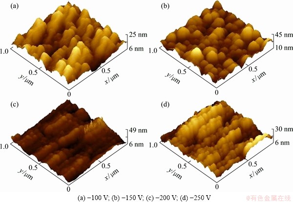
Fig. 5 AFM images of Cr-GLC-H film at different bias voltages
It might be related with the high energy of impinging ions to film growth that help improve the roughness by the surface diffusion [18].
3.3 Effect of substrate bias on tribological behavior of GLC films
The low friction coefficient and long wear life of GLC films play an important role for its industrial applications. Figure 6 shows the average friction coefficient of Cr-GLC-H films with different bias voltages. With the bias voltage increasing, it can be found an increase (up to maximum at -150 V) and subsequent decrease of the friction coefficient. The change trends of sp3 bond, surface roughness and friction coefficient with the increased bias voltages are the same in variation. The lowest surface roughness and lowest friction coefficient correspond to the highest sp3 with the Cr-GLC-H films at the bias voltage of -100 V. It should be noted here that the calculated wear rate of Cr-GLC-H films has the minimum value of 9.85��10-11 mm3/(N��m) at -100 V of bias voltage.
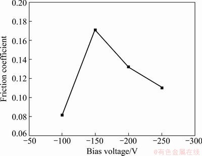
Fig. 6 Friction coefficients of Cr-GLC-H films deposited with different bias voltages
4 Conclusions
The GLC films were successfully deposited on HSS and silicon wafers by a hybrid HIPIMS with DC-MS technique. The results showed that Cr doping increased the content of the sp2 bonds, and hydrogen content would cause an increase of sp3-tpye bonding, With the bias voltage increased, it can be found a first increase (up to maximum at -150 V) and a subsequent decrease of sp3 bond, surface roughness as well as friction coefficient of Cr-GLC-H films. At the bias of -100 V, Cr-GLC-H films demonstrated a low friction coefficient and wear rate.
References
[1] NOVOSELOV K S, GEIM A K, MOROZOV S V, JIANG D, ZHENG Y, DUBONOS S V, GRIGORIEVA I V, FIRSOV A A. Electric field effect in atomically thin carbon films [J]. Science, 2004, 306(5696): 666-669.
[2] IIJIMA S. Helical microtubules of graphitic carbon [J]. Nature, 1991, 354(6348): 56-58.
[3] KROTO H W, HEATH J R, O��BRIEN S C, CRUL R F, SMALLEY R E. C60: buckminsterfullerene [J]. Nature, 1985, 318(6042): 162-163.
[4] WU G S, DAI W, ZHENG H, WANG A Y. Improving wear resistance and corrosion resistance of AZ31 magnesium alloy by DLC/AlN/Al coating [J]. Surface and Coatings Technology, 2010, 205: 2067-2073.
[5] ALAMI J, GUDMUNDSSON J T, BOHLMARK J, BRICH J, HELMERSSON U. Plasma dynamics in a highly ionized pulsed magnetron discharge [J]. Plasma Sources Science and Technology, 2005, 14: 525-527.
[6] GYLFASON K B, ALAMI J, HELMERSSON U, GUDMUNDSSON J T. Ion-acoustic solitary waves in a high power pulsed magnetron sputtering discharge [J]. Journal of Physics D, 2005, 38: 3417-3434.
[7] KOUZNETSOV V, MACAK K, SCHNEIDER J M, HELMERSSON U, PETROV I. A novel pulsed magnetron sputtering technique utilizing very high target power densities [J]. Surface and Coatings Technology, 1999, 122: 290-293.
[8] MACAK K, KOUZNETSOV V, SCHNEIDER J, HELMERSSON U, PETROV I. Ionized sputter deposition using an extremely high plasma density pulsed magnetron discharge [J]. Journal of Vacuum Science and Technology A, 2000, 18: 1533-1537.
[9] ANDERS A. Deposition rates of high power impulse magnetron sputtering: Physics and economics [J]. Journal of Vacuum Science and Technology A, 2010, 28: 783-790.
[10] TIAN X B, WU Z Z, SHI J W, LI X P, GONG C Z, YANG S Q. Development and discharge behavior of high power density pulse magnetron sputtering system [J]. Vacuum, 2010, 47: 44-47.
[11] HAERLE R, RIEDO E, PASQUARELLO A. sp2/sp3 hybridization ratio in amorphous carbon from C1s core-level shifts: X-ray photoelectron spectroscopy and first-principles calculation [J]. Physical Review B, 2001, 65: 045101.
[12] WELL R J, QUANT J. Radiative jet experiments of astrophysical interest using intense lasers [J]. Physical Review Letters, 1999, 83: 1982-1985.
[13] SINGH V, JIANG J C, MELETIES E I. Cr-diamond like carbon nanocomposite films: Synthesis, characterization and properties [J]. Thin Solid Films, 2005, 489: 150-158.
[14] CASIRAGHI C, FERRARI A C, ROBERSTON J. Raman spectroscopy of hydrogenated amorphous carbons [J]. Physical Review B, 2005, 72: 085401.
[15] FERRARI A C, ROBERSTON J. Resonant Raman spectroscopy of disordered, amorphous, and diamond like carbon [J]. Physical Review B, 2001, 62: 075414.
[16] CASIRAGHI C, PIAZZA F, FERRARI A C, GRAMBOLE D, ROBERTSON J. Bonding in hydrogenated diamond-like carbon by Raman spectroscopy [J]. Diamond and Related Materials, 2005, 14: 1098-1102.
[17] ROBERSTON J. Diamond-like amorphous carbon [J]. Materials Science and Engineering R, 2002, 37(4/6): 129-281.
[18] WANG P, WANG X, CHEN Y M, ZHANG G, LIU W M, ZHANG J Y. The effect of applied negative bias voltage on the structure of Ti-doped a-C:H films deposited by FCVA [J]. Applied Surface Science, 2007, 253: 3722-3726.
(Edited by HE Xue-feng)
Foundation item: Project (51005226) supported by the Natural Science Foundation of China; Project (2010A610161) supported by the Natural Science Foundation of Ningbo Government, China; Project (2010D10015) supported by the International Cooperation Foundation of Ningbo Government, China
Corresponding author: KE Pei-ling; Tel: +86-574-86685036; E-mail: kepl@nimte.ac.cn
DOI: 10.1016/S1003-6326(12)61797-X
Abstract: The Cr-doped hydrogen-GLC films were prepared by a hybrid magnetron sputtering system composed of a direct current magnetron sputtering (DC-MS) source of carbon and a high power impulse magnetron sputtering (HIPIMS) source of Cr with reactive gas of C2H2. The hydrogen-free GLC and Cr-doped GLC films were also prepared for comparison. The influence of substrate bias on the Cr-doped hydrogen-GLC films was investigated. With the increase of substrate bias from -100 V to -250 V, the re-sputtering of weak bonding sp2 firstly occurred and induced an increased sp3 bonding. However, the following sp3 to sp2 transformation resulted in a decreased sp3 bonding. The change trends of surface roughness and friction coefficient with the increased bias voltages were the same as those of sp3 bond. The lowest surface roughness and lowest friction coefficient corresponded to the highest sp3 with the Cr-GLC-H films at the bias voltage of -100 V.
