
Trans. Nonferrous Met. Soc. China 25(2015) 1935-1943
Surface modification of Cu-25Cr alloy induced by high current pulsed electron beam
Zhi-ming ZHOU1, Lin-jiang CHAI1, Zhi-pei XIAO1, Jian TU1, Ya-ping WANG2, Wei-jiu HUANG1
1. School of Materials Science and Engineering, Chongqing University of Technology, Chongqing 400054, China;
2. School of Science, Xi��an Jiaotong University, Xi��an 710049, China
Received 18 August 2014; accepted 13 November 2014
Abstract:
A Cu-25Cr alloy prepared by vacuum induction melting method was treated by the high current pulsed electron beam (HCPEB) with pulse numbers ranging from 1 to 100. Surface morphologies and microstructures of the alloy before and after the treatment were investigated by scanning electron microscopy and X-ray diffraction. The results show that significant surface modification can be induced by HCPEB with the pulse number reaching 10. Craters with typical morphologies on the Cu-25Cr alloy surface are formed due to the dynamic thermal field induced by the HCPEB. Micro-cracks, as a unique feature, are well revealed in the irradiated Cu-25Cr specimens and attributed to quasi-static thermal stresses accumulated along the specimen surface. The amount of cracks is found to increase with the pulse number and a preference of these cracks to Cr phases rather than Cu phases is also noted. Another characteristic produced by the HCPEB is the fine Cr spheroids, which are determined to be due to occurrence of liquid phase separation in the Cu-25Cr alloy. In addition, an examination on surface roughness of all specimens reveals that more pulses will produce a roughened surface, as a result of compromising the above features.
Key words:
Cu-Cr alloy; surface modification; high current pulsed electron beam; microstructure;
1 Introduction
Due to an excellent combination of mechanical properties and electrical conductivity, Cu-Cr alloys have found important applications as contact materials in medium-voltage and high-current vacuum interrupters [1]. Earlier studies [2,3] revealed that the actual performance of Cu-Cr contacts could be greatly affected by their microstructure, especially the grain size and distribution of Cr phases. Generally, Cu-Cr alloys with large and segregated Cr phases have inferior properties compared with those with fine and uniformly distributed Cr grains.
Traditional methods for preparing Cu-Cr alloys include powder metallurgy from densification of mixed Cu-Cr powders [4], infiltration of Cu into Cr matrix [5], and arc melting of Cr and Cu in low pressure argon atmosphere [1]. These techniques are often blamed for either poor abilities to limit the size of Cr phases or high complexity and cost. Hence, researchers are motivated to explore new flexible techniques with the capability of obtaining optimized microstructures for Cu-Cr alloys effectively. Nowadays, a variety of novel techniques, such as mechanical alloying [6], melt spinning [7], vacuum induction melting [8], and electromagnetic levitation and splat-quenching [9], have been successfully applied to the preparation of Cu-Cr alloys. Enhanced performance is thus achieved through microstructure optimization, which can to a large extent be attributed to the effective control of these methods on Cr phase sizes.
Along with the unceasing efforts of exploring new preparation methods, attention has recently also been paid to the effects of surface treatments on Cu-Cr alloys by a few investigators [10-13]. This is because the surfaces of many engineering materials, including Cu-Cr alloys, are frequently the sites where failures prefer to occurring. Among various techniques used for surface treatments, high current pulsed electron beam (HCPEB) is a relatively new but very advantageous technique due to its high efficiency, simplicity and reliability [14-16]. During the HCPEB irradiation, a dynamic temperature field would be generated near the surface of materials, featured by super fast heating (even melting or evaporating) and cooling. In the meantime, there also exists a dynamic stress field that could cause intense deformation on the material surface. Due to such combined effects, the HCPEB is able to substantially modify the surface characteristics and then possibly improve properties of the irradiated materials.
To date, there have been a number of successful applications of the HCPEB technique to various metals and alloys, such as stainless steels [17-19], Al alloys [16,20,21], Mg alloys [22,23], Ti alloys [24-28] and intermetallics [29,30]. With careful selection of operation parameters, greatly improved corrosion resistance, wear resistance and mechanical properties were obtained by different researchers, clearly indicating its large potential. However, few efforts have been made to examine the surface modification effect of this technique on Cu-Cr alloys, except a recent attempt by LAMPERTI et al [10,11]. By use of secondary ion mass spectrometry and atomic force microscopy, they reported the formation of some Cu1-x-Crx compounds, unattainable by other methods, on the surface of a HCPEB-treated Cu-30Cr alloy. In the current investigation, we will further study the effect of HCPEB treatment on the surface modification of a Cu-25Cr alloy, and present in detail the microstructural evolution of the material surface with different irradiation numbers.
2 Experimental
The starting material employed in this work was a Cu-25Cr (mass fraction, %) alloy prepared by vacuum induction melting (VIM). Details on its preparation could be found elsewhere [8]. Specimens with dimensions of d20 mm �� 5 mm were cut from the as-prepared Cu-25Cr alloy. Prior to HCPEB treatment, these specimens were ground using SiC abrasive papers and polished with diamond paste. A RT-2M type HCPEB source was employed to irradiate the surfaces of the as-polished specimens, with various pulse numbers of 1, 10, 30, 50 and 100. The HCPEB treatments were performed under the following conditions: the electron energy 30 keV, the pulse duration 2 ��s, energy density about 14 J/cm2, and vacuum 1��10-2 Pa.
Surface microstructures of the specimens before and after the HCPEB treatment were characterized by a JEOL JSM-6460LV scanning electron microscope (SEM). Both secondary electron and backscattered electron images were taken to reveal different characteristics of the surface microstructures. An energy dispersive spectroscopy (EDS) attached to the SEM was also employed to analyze chemical compositions of local positions. In addition, the phase constituents of all specimens were determined by a conventional X-ray diffractometer (DX-2500) using Cu K�� radiation.
3 Results and discussion
3.1 Before HCPEB treatment
The microstructures of the starting (as-prepared) material are shown in Fig. 1. Figure 1(a) shows a secondary electron image taken from the specimen surface, etched in a mixed solution to reveal the morphology of Cr phases. One can see that a number of Cr phases showing round or elliptical shapes are densely distributed in the matrix of Cu phase. In earlier work [8] coarse dendrites were reported to be the main feature of the Cr phases in VIM-prepared Cu-25Cr alloys. In fact, the discrepancy is just due to a stereological effect, that is, the round or elliptical shapes in Fig. 1(a) corresponding to the cross sections of the Cr dendrites. The lengthwise section of some Cr dendrites can also be seen, as marked in Fig. 1(a), which is helpful to envision their global shapes.

Fig. 1 Surface microstructures revealed by secondary electron (a) and backscattered electron (b) images, and cross-section morphology (c) of starting material
Figure 1(b) shows a backscattered electron (BSE) image of the as-prepared Cu-25Cr alloy. Thanks to the intrinsic property of backscattered electrons, heavy elements (high atomic number) have brighter contrast than light elements (low atomic number) in a BSE image. This is known as atomic number or Z-contrast of backscattered electrons. In the present case, the atomic number of Cr (Z=24) is significantly lower than that of Cu (Z=29). Therefore, the Cr phases are darker in Fig. 1(b), compared with the Cu phases. From Fig. 1(b), one can also note that there are clear and sharp boundaries between those bright and dark contrasts, separating the Cr- and Cu-phases. In fact, this is a general feature for Cu-Cr alloys obtained under an equilibrium condition, as a result of the very limited mutual solubility (near zero at room temperature) between the two constituents [31]. In addition, the grain size of the Cr phases, widely acknowledged as a key parameter for this kind of materials, can be estimated from Fig. 1(b). Measurements by the linear intercept method reveal that the majority of the grain sizes (more precisely, diameters of cross sections of Cr dendrites) lie in the range of 20-40 ��m. The cross-section morphology of the starting material is shown in Fig. 1(c), with its surface being well prepared for HCPEB treatment. It can be seen that the surface of the unirradiated specimen is relatively smooth, thus suggesting a small roughness.
Results of an XRD examination for the as-prepared Cu-25Cr alloy are shown in Fig. 2. It can be seen that all detected peaks could be successfully indexed by elementary Cu and Cr, indicating the absence of any other phases.

Fig. 2 XRD patterns of specimens with or without HCPEB treatment
3.2 After HCPEB treatment
Figure 2 also shows the XRD patterns obtained for specimens HCPEB-treated for various pulses. Under various conditions, it seems that all irradiated specimens have almost the same peak profiles as the unirradiated specimen. Although the X-ray diffraction intensity is presented in a logarithmic unit, best for resolving minor phases, no peaks corresponding to any new phases can be clearly differentiated from the background. This provides a strong implication that phase alteration would not occur during irradiating the Cu-25Cr alloy by the HCPEB.
BSE images of surfaces of the specimens treated by the HCPEB for various pulse numbers are displayed in Fig. 3. From Fig. 3(a), one can see that the microstructure of the specimen with one shot is not significantly changed, compared with that of the initial specimen (Fig. 1(b)). Sharp interfaces between Cr and Cu phases remain clear and the integrities of almost all Cr phases are also maintained. As the pulse number increases to 10, remarkable changes on microstructure can be noticed, as shown in Fig. 3(b). Clearly, most Cr phases are heavily damaged by the electron beam irradiation, evidenced first by loss of prior regular shapes. Near-edge parts of these prior Cr phases seem to be blasted away, with irregular-shape residual Cr phases left. Meanwhile, a few cracks are also observed in some Cr phases, as indicated by arrows in Fig. 3(b). With further increasing the pulse number from 10 to 50, microstructural modification caused by the electron beam is more evident (Fig. 3(c)). Edges of the prior Cr phases seem to be well ��dissolved�� into the Cu matrices, which produce a visual effect of amount reduction of Cr phases. In addition, there are more cracks existing in Cr phases. For the specimen HCPEB-treated for 100 pulses, its microstructural characteristics closely resemble those with 50 pulses, except denser cracks in Cr phases (Fig. 3(d)).
Apart from bulk Cr phases (original Cr dendrites), many small Cr-rich spheroids (or particles) are also found in irradiated specimens. An example is given in Fig. 4, which is a secondary electron image of HCPEB-treated specimen for 30 pulses. Sizes of these spheroids are limited to a few micrometers, greatly lower than those of bulk Cr phases (see the spheroid indicated by an arrow and its neighboring bulk Cr phase). A composition measurement for the arrowed spheroid reveals 34.43% Cr and 65.57% Cu (mole fraction). In consideration of the small size of the spheroid, most of the detected Cu signals should result from the alloy matrix. Since the XRD results in Fig. 2 confirm that there are no new phases formed after HCPEB treatment, these spheroids can be determined to be Cr phases. In fact, a liquid phase separation (LPS) phenomenon is often reported for Cu-Cr alloys [7,9,32-35], because of the existence of a liquid miscibility gap in such a binary phase diagram. One direct result of the LPS is the formation of fine Cr-rich spheroids, which are very similar to those revealed in the present work.
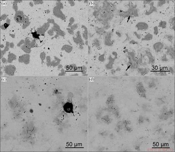
Fig. 3 Backscattered electron images of surfaces of specimens HCPEB-treated for 1 pulse (a), 10 pulses (b), 50 pulses (c) and 100 pulses (d)

Fig. 4 Morphology (a) and composition (b) of fine Cr-rich spheroids in specimen HCPEB-treated for 30 pulses
A special surface morphology showing craters, was often reported in many HCPEB-treated metal materials [36,37]. As shown in Fig. 5, the present experiment reveals that craters can also be induced by the HCPEB treatment in the Cu-25Cr alloy. Figures 5(a) and (b) show the morphologies of craters formed in specimens HCPEB-treated for 30 and 50 pulses, respectively. The two craters in Fig. 5 are both located in Cr phases, evidenced by the presence of cracks and EDS analyses (not shown here). These craters, generally with round edge, could be easily discriminated from Cr phase matrices with serrated boundaries. Sizes of these craters, confined by the parent Cr phases, range from a few to more than ten micrometers. Another interesting result in Fig. 5(a) is cracks formed within the crater, as indicated by a white arrow. To differentiate them from those (indicated by a black arrow and hereinafter denoted as primary cracks) formed earlier in parent Cr phases, they are referred to as secondary cracks.
Figure 6 shows the evolution of cross-section morphologies in HCPEB-treated specimens. In regard to surface roughness of these specimens, a clear uptrend could be revealed from Fig. 6. For the specimen with a single HCPEB shot, a smooth surface is obtained in Fig. 6(a), compared with the unirradiated specimen (Fig. 1(c)). This is consistent with the result revealed in Fig. 3(a), which indicates very weak influence of the only one pulse on the alloy microstructure. For the specimen treated for 10 pulses, Fig. 6(b) reveals a clear roughening surface. This may correspond to the micro- structural change (such as cracks in Cr phases) as seen in Fig. 3(b). For specimens irradiated further heavily (for 50 and 100 pulses), Figs. 6(c) and (d) exhibit that the surfaces of both specimens are greatly roughened.

Fig. 5 Surface craters in specimens HCPEB-treated for 30 (a) and 50 (b) pulses

Fig. 6 Cross-section morphologies of specimens HCPEB-treated for 1 pulse (a), 10 pulses (b), 50 pulses (c) and 100 pulses (d)
4 Discussion
4.1 Craters
For many metal materials treated by electron beams, craters are often reported as a general characteristic, similar to those observed in the present work. By conducting both computer simulation and experimental examination, QIN et al [37] demonstrated that such morphologies are the results of local subsurface melting and erupting through the solid outer surface. Furthermore, a variety of structural defects near surface are also believed to be able to facilitate the formation of craters. For example, POGREBNJAK et al [38] reported that locations with vacancy cluster agglomeration could act as ����weak���� points where the eruptions occur more easily. In parallel work, ZOU et al [19,36] figured out that carbides or sulfides in steels were always the nucleation sites for craters. Eruptions of these second phase particles had a major contribution to improved corrosion resistance of the HCPEB-treated steels due to a selective surface purification mechanism.
For the Cu-25Cr alloy used in this study, small intermetallic particles are not expected to be present, as revealed by the XRD result in Fig. 2. Therefore, reasons for the formation of craters in Cr and Cu phases should not be attributed to the mechanism proposed by ZOU et al [19,36]. Very recently, ZHANG et al [39] have presented a detailed microstructural examination on a commercially pure Cu treated by the HCPEB. Abundant vacancy defects were found to be introduced into the subsurface layer of Cu during irradiation, which is consistent with the work of POGREBNJAK et al [38]. Therefore, it is reasonable to believe that vacancies should also be responsible for the crater formation in the irradiated Cu-25Cr alloy.
4.2 Cracks
As demonstrated above, the existence of surface cracks is also a common feature in the Cu-25Cr alloy treated by the HCPEB, which are definitely detected in all irradiated specimens with pulse number beyond 10. Clearly, such cracks are products of the employed electron beam treatment. Their absence in the one-pulse treated specimens further suggests that these cracks have a minimum requirement on the pulse number. It is interesting to notice that cracks in Cr phases were also detected in HCPEB-treated Cu-30Cr alloy by LAMPERTI et al [10,11].
To reveal the in-depth reason accounting for these cracks, it is necessary to perform a stress analysis for the irradiated specimens. During the pulsed electron beam irradiation, two types of stresses are known to be induced, i.e., the thermo-elastic stress and the quasi-static thermal stress [15]. The thermo-elastic stress results from rapid elastic deformation caused by a large temperature gradient towards the substrate, thus having a propagation direction parallel to the electron beam. The quasi-static stress, however, is produced by the confinement on the surface layer against the difference of lateral thermal deformation, with its direction perpendicular to the electron beam. The magnitudes of both types of stresses have been well investigated by earlier researchers [15,40]. The thermo-elastic stress was reported to have a low magnitude in the order of 0.1 MPa. It is negligible compared with that of the quasi-static stress, which can easily reach several hundreds of MPa or even a few GPa. Such values are higher than yield limits of most pure metals and some high strength alloys. Thus, the quasi-static stress is generally determined to be the cause of intense plastic deformation on the surfaces of various HCPEB-treated materials [22,23,40], and must be responsible for the cracks in the irradiated Cu-25Cr alloy.
In regards to the fact that cracks prefer Cr phases to Cu phases, the difference on crystal structures between both phases could be noted. Metals with a body centered cubic (BCC) structure, such as Cr, generally possess inferior ability to accommodate plastic strain, compared with metals like Cu with a face centered cubic (FCC) structure. As a result of strain accommodation failure, cracks would preferably appear in Cr phases, as revealed in the present work (Fig. 3).
Figure 5 presents an evidence of dynamic formation of the cracks during the electron beam irradiation. When a critical stress is accumulated after several pulses, primary cracks appear in bulk Cr phases. As the pulse number increases, an eruption event occurs, during which molten Cr phases are sprayed on nearby solid Cr matrix. Although the erupted molten Cr may cover some primary cracks (see Fig. 5(a)), new (secondary) cracks would be produced within the craters by subsequent irradiation. Such an analysis indicates that cracks in Cr phases induced by the HCPEB could not be self-healed or repaired by increasing pulse numbers.
4.3 Liquid phase separation
Thanks to the existence of a liquid miscibility gap in the Cu-Cr binary phase diagram, the LPS could occur once a Cu-Cr liquid is undercooled into the gap. The gap width was reported to be broad. For example, a recent experimental investigation on Cu-Cr alloys prepared by electromagnetic levitation and splat quenching verified the occurrence of the LPS in melts with Cr contents ranging from 5% to 70% (mole fraction) [35]. Clearly, the composition of the present alloy lies in the range allowing LPS.
Another important factor to be concerned is cooling condition selected for melts. For Cu-Cr alloys with Cr contents lower than 50%, such as in the present case, the miscibility gap is thermodynamically metastable [34]. Thus, a high cooling rate is required to allow the Cu-Cr liquid to drop into the miscibility gap and then separate into two new liquids. As the minor constituent, each separated liquid Cr phase prefers to forming a spherical shape to minimize individual surface energy. In the sequence, the rapid cooling would suppress the growth of the small Cr spheroids into dendrites and solidify them soon. As a result, fine Cr spheroids with sizes of a few micrometers or lower can be detected by microstructural observation and are generally regarded as a direct evidence of the occurrence of the LPS [7,9,32-35]. Otherwise, a slow cooling would lead to an equilibrium or quasi-equilibrium solidification microstructure with coarse Cr dendrites presented [9].
It is to be noticed that a super fast cooling rate, higher than 1��107 ��C/s [15,37], would be reached for surface melting layer in HCPEB-treated materials. At such a high cooling rate, a large supercooling is inevitable. As for the Cu-25Cr alloy in this study, the employed HCPEB treatment could easily undercool the surface of Cu-Cr melt into its liquid miscibility gap and then trigger the LPS. Based on the above analysis, fine Cr spheroids revealed in Fig. 4 can be confirmed to be direct evidences of the LPS in the irradiated Cu-25Cr alloy.
In an earlier attempt, LAMPERTI et al [10,11] claimed that Cu1-x-Crx compound was formed in a Cu-30Cr alloy treated by similar HCPEB treatment. By employing secondary ion mass spectrometry, they presented some evidences that Cr and Cu could be concurrently enriched in many sites. They also made a simple estimation on possible reaction kinetics and believed that the formation of the Cu1-x-Crx compound was possible under the non-equilibrium condition created by the HCPEB. Nevertheless, more convincing evidence verifying the existence of the Cu1-x-Crx compound, such as its crystallographic information, was not provided by them. On the contrary to their conclusion, no such Cu1-x-Crx compounds are detected in our study, as suggested by the XRD result in Fig. 2. In fact, it was already demonstrated [41] that formation enthalpies of Cu1-x-Crx compounds were positive over the entire composition range, suggesting a low possibility for the existence of such compounds. Therefore, we suggest that the Cu1-x-Crx compound reported by LAMPERTI et al [10,11] is treated with caution in future work.
In addition, with respect to the simultaneous enrichment of Cr and Cu in many sites in experimental result in Refs. [10,11], a likely explanation points to supersaturation of Cu into Cr phases caused by the rapid cooling. There have been a number of studies reporting enhanced mutual solubility between Cr and Cu by various rapid solidification methods [32,42-44]. For example, 12% Cu was detected in LPS-induced Cr spheroids of Cu-Cr alloys after a vacuum breakdown test [32]. Similar cases could be expected for the LPS- induced Cr spheroids in the present work, as revealed in Fig. 4 (Cu is overestimated due to the matrix contribution). Another clear evidence of enhanced mutual solubility in the present work is the disappearance of originally distinct interface between Cu and Cr phases after heavy HCPEB irradiation (Figs. 2(c) and (d)). Instead of sharp separation, gradual transition regions with a compromised contrast, suggesting coexistence of Cr and Cu, appear from the dark Cr phases to the bright Cu phases.
4.4 Roughness and others
Roughness is often regarded as a direct indicator of surface quality of engineering materials and thus has received much attention from researchers. In earlier studies [22,25,45] on HCPEB-treated materials, both surface smoothening and roughening effects were reported, largely depending on irradiation conditions and intrinsic properties of selected materials. Specifically, for the Cu-25Cr alloy under the irradiation condition selected in the present work, the surface is always roughened with increasing pulse numbers (Fig. 6). Generally, the amount of craters induced by the HCPEB is believed to have a close relation with the surface roughness. For instance, an investigation by GAO et al [22] on HCPEB-treated Mg alloys revealed that more pulses could suppress the formation of craters and thus gave rise to smoother surfaces. In our work, however, a clear reduction of crater numbers is not observed for irradiated Cu-25Cr alloy for more pulses. In contrast, cracks, another unique feature induced by the HCPEB, are found to be denser with increasing pulse number. As demonstrated in Section 4.2, cracks can be consecutively produced by different pulses and are hard to be eliminated. Therefore, it should be reasonable to ascribe mainly the roughened surfaces to the accumulation of cracks.
Direct examinations on various properties changed by the HCPEB treatment are still ongoing and will be reported in the near future. Nevertheless, based on the results presented in this work, a tentative discussion can be given in advance. Size refinement of Cr phases is generally known to be desirable for improving the dielectric strength of Cu-Cr alloys. Hence, fine Cr spheroids produced by the HCPEB treatment should bring some beneficial effects for Cu-Cr alloys as contact materials. Concomitantly, however, the HCPEB treatment could also induce some unfavorable products, such as craters and cracks, which destroy surface integrities of specimens. To what extent that such beneficial and detrimental effects will offset each other could be answered only after the comprehensive property examinations.
5 Conclusions
1) The HCPEB is capable of inducing remarkable surface modifications for the Cu-25Cr alloy.
2) Typical craters can be induced by the HCPEB treatment in the Cu-25Cr alloy.
3) A unique feature, cracks in Cr phases, is found in irradiated specimens and attributed to quasi-static thermal stresses accumulated along the specimen surface.
4) The occurrence of liquid phase separation in the HCPEB-treated specimens is confirmed by the presence of fine Cr spheroids.
5) A surface roughening effect of the HCPEB treatment on the Cu-25Cr alloy is revealed.
References
[1] SLADE P G. Advances in material development for high power, vacuum interrupter contacts [J]. IEEE Transactions on Components Packaging and Manufacturing Technology: Part A, 1994, 17: 96-106.
[2] WANG Y P, DING B J. The preparation and the properties of microcrystalline and nanocrystalline CuCr contact materials [J]. IEEE Transactions on Components and Packaging Technologies, 1999, 22: 467-472.
[3] WANG You-hong, SONG Xiao-ping, SUN Zhan-bo, ZHOU Xuan, GUO Juan. Effects of Ti addition on microstructures of melt-spun CuCr ribbons [J]. Transactions of Nonferrous Metals Society of China, 2007, 17(1): 72-76.
[4] DING B J, YANG Z M, WANG X T. Influence of microstructure on dielectric strength of CuCr contact materials in a vacuum [J]. IEEE Transactions on Components Packaging and Manufacturing Technology: Part A, 1996, 19: 76-81.
[5] ZHOU Zhi-ming, WANG Ya-ping, XIA Hua, ZHAN Jie. Research development of manufacture processing of Cu-Cr alloy [J]. Materials Review, 2008, 22: 44-47. (in Chinese)
[6] MORRIS D G, MORRIS M A. Rapid solidification and mechanical alloying techniques applied to Cu-Cr alloys [J]. Materials Science and Engineering A, 1988, 104: 201-213.
[7] ZHOU Z M, WANG Y P, GAO J, KOLBE M. Microstructure of rapidly solidified Cu-25wt.% Cr alloys [J]. Materials Science and Engineering A, 2005, 398: 318-322.
[8] ZHANG C, WANG Y, YANG Z, GUO Y, BINGJUN D, Microstructure and properties of vacuum induction melted CuCr25 alloys [J]. Journal of Alloys and Compounds, 2004, 366: 289-292.
[9] GAO J, WANG Y P, ZHOU Z M, KOLBE M. Phase separation in undercooled Cu-Cr melts [J]. Materials Science and Engineering A, 2007, 449-451: 654-657.
[10] LAMPERTI A, OSSI P M, ROTSHTEIN V P. Surface analytical chemical imaging and morphology of Cu-Cr alloy [J]. Surface and Coatings Technology, 2006, 200: 6373-6377.
[11] LAMPERTI A, OSSI P M. SIMS direct surface imaging of Cu1-xCrx formation [J]. Applied Surface Science, 2006, 252: 2288-2296.
[12] GENG H R, LIU Y, CHEN C Z, SUN M H, GAO Y Q. Laser surface remelting of Cu-Cr-Fe contact material [J]. Materials Science and Technology, 2000, 16: 564-567.
[13] HIROSE A, KOBAYASHI K F. Surface alloying of cupper with chromium by CO2 laser [J]. Materials Science and Engineering A, 1994, 174: 199-206.
[14] PROSKUROVSKY D I, ROTSHTEIN V P, OZUR G E, MARKOV A B, NAZAROV D S, SHULOV V A, IVANOV Y F, BUCHHEIT R G. Pulsed electron-beam technology for surface modification of metallic materials [J]. Journal of Vacuum Science & Technology A, 1998, 16: 2480-2488.
[15] PROSKUROVSKY D I, ROTSHTEIN V P, OZUR G E, IVANOV Y F, MARKOV A B. Physical foundations for surface treatment of materials with low energy, high current electron beams [J]. Surface and Coatings Technology, 2000, 125: 49-56.
[16] ZHAO Tie-jun, TIAN Xiao-mei, GAO Bo, TU Gan-feng. Research development of electron beam surface treatment [J]. Materials Review, 2009, 23: 89-91. (in Chinese)
[17] ZOU J X, ZHANG K M, GROSDIDIER T, DONG C, QIN Y, HAO S Z, YANG D Z. Orientation-dependent deformation on 316L stainless steel induced by high-current pulsed electron beam irradiation [J]. Materials Science and Engineering A, 2008, 483-484: 302-305.
[18] ZHANG K, ZOU J, GROSDIDIER T, DONG C, YANG D. Improved pitting corrosion resistance of AISI 316L stainless steel treated by high current pulsed electron beam [J]. Surface and Coatings Technology, 2006, 201: 1393-1400.
[19] ZOU J, ZHANG K, DONG C, QIN Y, HAO S, GROSDIDIER T. Selective surface purification via crater eruption under pulsed electron beam irradiation [J]. Applied Physics Letters, 2006, 89: 041913.
[20] HAO Y, GAO B, TU G F, CAO H, HAO S Z, DONG C. Surface modification of Al-12.6Si alloy by high current pulsed electron beam [J]. Applied Surface Science, 2012, 258: 2052-2056.
[21] HAO Y, GAO B, TU G F, LI S W, HAO S Z, DONG C. Surface modification of Al-20Si alloy by high current pulsed electron beam [J]. Applied Surface Science, 2011, 257: 3913-3919.
[22] GAO B, HAO S, ZOU J, GROSDIDIER T, JIANG L, ZHOU J, DONG C. High current pulsed electron beam treatment of AZ31 Mg alloy [J]. Journal of Vacuum Science & Technology A, 2005, 23: 1548-1553.
[23] HAO S, GAO B, WU A, ZOU J, QIN Y, DONG C, AN J, GUAN Q. Surface modification of steels and magnesium alloy by high current pulsed electron beam [J]. Nuclear Instruments and Methods in Physics Research: Section B, 2005, 240: 646-652.
[24] GAO Y K. Influence of pulsed electron beam treatment on microstructure and properties of TA15 titanium alloy [J]. Applied Surface Science, 2013, 264: 633-635.
[25] GAO Y K. Surface modification of TC4 titanium alloy by high current pulsed electron beam (HCPEB) with different pulsed energy densities [J]. Journal of Alloys and Compounds, 2013, 572: 180-185.
[26] ZHANG X D, ZOU J X, WEBER S, HAO S Z, DONG C, GROSDIDIER T. Microstructure and property modifications in a near �� Ti alloy induced by pulsed electron beam surface treatment [J]. Surface and Coatings Technology, 2011, 206: 295-304.
[27] ZHANG X D, HAO S Z, LI X N, DONG C, GROSDIDIER T. Surface modification of pure titanium by pulsed electron beam [J]. Applied Surface Science, 2011, 257: 5899-5902.
[28] GAO Y K. Surface modification of TA2 pure titanium by low energy high current pulsed electron beam treatments [J]. Applied Surface Science, 2011, 257: 7455-7460.
[29] GROSDIDIER T, ZOU J X, STEIN N, BOULANGER C, HAO S Z, DONG C. Texture modification, grain refinement and improved hardness/corrosion balance of a FeAl alloy by pulsed electron beam surface treatment in the ��heating mode�� [J]. Scripta Materialia, 2008, 58: 1058-1061.
[30] ZHANG K M, YANG D Z, ZOU J X, GROSDIDIER T, DONG C. Improved in vitro corrosion resistance of a NiTi alloy by high current pulsed electron beam treatment [J]. Surface and Coatings Technology, 2006, 201: 3096-3102.
[31] BI Li-ming, LIU Ping, CHEN Xiao-hong, LIU Xin-kuan, LI Wei, MA Feng-cang. Analysis of phase in Cu-15%Cr-0.24%Zr alloy [J]. Transactions of Nonferrous Metals Society of China, 2013, 23: 1342-1348.
[32] WEI X, WANG J, YANG Z, SUN Z, YU D, SONG X, DING B, YANG S. Liquid phase separation of Cu-Cr alloys during the vacuum breakdown [J]. Journal of Alloys and Compounds, 2011, 509(25): 7116-7120.
[33] SUN Zhan-bo, WANG Yao-hong, GUO Juan. Liquid phase separation of Cu-Cr alloys during rapid cooling [J]. Transactions of Nonferrous Metals Society of China, 2006, 16: 998-1002.
[34] ZHOU Z M, GAO J, LI F, WANG Y P, KOLBE M. Experimental determination and thermodynamic modeling of phase equilibria in the Cu-Cr system [J]. Journal of Materials Science, 2011, 46: 7039-7045.
[35] ZHOU Z M, GAO J, LI F, ZHANG Y K, WANG Y P, KOLBE M. On the metastable miscibility gap in liquid Cu-Cr alloys [J]. Journal of Materials Science, 2009, 44: 3793-3799.
[36] ZOU J, GROSDIDIER T, ZHANG K, DONG C. Mechanisms of nanostructure and metastable phase formations in the surface melted layers of a HCPEB-treated D2 steel [J]. Acta Materialia, 2006, 54: 5409-5419.
[37] QIN Y, DONG C, WANG X, HAO S, WU A, ZOU J, LIU Y. Temperature profile and crater formation induced in high-current pulsed electron beam processing [J]. Journal of Vacuum Science & Technology A, 2003, 21: 1934-1938.
[38] POGREBNJAK A D, MIKHALIOV A D, POGREBNJAK N A, TSVINTARNAYA Y V, LAVRENTIEV V I, ILJASHENKO M, VALYAEV A N, BRATUSHKA S, ZECCA A, SANDRIK R. Evolution of vacancy defects and dislocations in surface layers of iron as a result of pulsed electron beam treatment [J]. Physics Letters A, 1998, 241: 357-363.
[39] ZHANG Z, YANG S, LV P, LI Y, WANG X, HOU X, GUAN Q. The microstructures and corrosion properties of polycrystalline copper induced by high-current pulsed electron beam [J]. Applied Surface Science, 2014, 294: 9-14.
[40] QIN Y, ZOU J, DONG C, WANG X, WU A, LIU Y, HAO S, GUAN Q. Temperature�Cstress fields and related phenomena induced by a high current pulsed electron beam [J]. Nuclear Instruments and Methods in Physics Research Section B, 2004, 225: 544-554.
[41] KAUFMAN L. Coupled phase diagrams and thermochemical data for transition metal binary systems��III [J]. CALPHAD, 1978, 2: 117-146.
[42] SUN Z, ZHANG C, ZHU Y, YANG Z, DING B, SONG X. Microstructures of melt-spun Cu100-x�CCrx (x=3.4-25) ribbons [J]. Journal of Alloys and Compounds, 2003, 361: 165-168.
[43] CORREIA J B, DAVIES H A, SELLARS C M. Strengthening in rapidly solidified age hardened Cu-Cr and Cu-Cr-Zr alloys [J]. Acta Materialia, 1997, 45: 177-190.
[44] MORRIS M A, MORRIS D G. Microstructures and mechanical properties of rapidly solidified Cu-Cr alloys [J]. Acta Metallurgica, 1987, 35: 2511-2522.
[45] ZOU J X, ZHANG K M, HAO S Z, DONG C, GROSDIDIER T. Mechanisms of hardening, wear and corrosion improvement of 316L stainless steel by low energy high current pulsed electron beam surface treatment [J]. Thin Solid Films, 2010, 519: 1404-1415.
Cu-25Cr�Ͻ��ǿ������������������
��־��1�����ֽ�1��Ф־��1��Ϳ ��1������ƽ2����ΰ��1
1. ����������ѧ ���Ͽ�ѧ�빤��ѧԺ������ 400054��
2. ������ͨ��ѧ ��ѧԺ������ 710049
ժ Ҫ������ǿ�����������(HCPEB)��������ո�Ӧ�������Ʊ���Cu-25Cr�Ͻ���б�����Դ�������ѡ�õ����������ΧΪ1~100������ɨ��羵��X�������似����HCPEB����ǰ����Ʒ�������ò������֯�����о��������ʾ��������������ӵ�10�κ���Ʒ������ò�ᷢ�������仯����HCPEB�����������������Ķ�̬�¶ȳ�ʹCu-25Cr�Ͻ�����γɵ��͵��ۿ���֯��ͬʱ���ù��������ۻ�����̬��Ӧ����������Ʒ����������ƣ���������������������Ӷ��������⣬HCPEB������ʹCu-25Cr�Ͻ���淢��Һ���������������ϸС��Cr��������������֯���ۺ������£���Ʒ����Ĵֲڶ���������������Ӷ�������
�ؼ��ʣ�Cu-Cr�Ͻ𣻱�����ԣ�ǿ�����������������֯
(Edited by Wei-ping CHEN)
Foundation item: Projects (51101177, 51401040, 51171146, 51171216) supported by the National Natural Science Foundation of China; Project (CSTC2012JJA245) supported by the Natural Science Foundation of Chongqing, China
Corresponding author: Lin-jiang CHAI; Tel: +86-23-62563178; E-mail: chailinjiang@cqut.edu.cn
DOI: 10.1016/S1003-6326(15)63801-8
Abstract: A Cu-25Cr alloy prepared by vacuum induction melting method was treated by the high current pulsed electron beam (HCPEB) with pulse numbers ranging from 1 to 100. Surface morphologies and microstructures of the alloy before and after the treatment were investigated by scanning electron microscopy and X-ray diffraction. The results show that significant surface modification can be induced by HCPEB with the pulse number reaching 10. Craters with typical morphologies on the Cu-25Cr alloy surface are formed due to the dynamic thermal field induced by the HCPEB. Micro-cracks, as a unique feature, are well revealed in the irradiated Cu-25Cr specimens and attributed to quasi-static thermal stresses accumulated along the specimen surface. The amount of cracks is found to increase with the pulse number and a preference of these cracks to Cr phases rather than Cu phases is also noted. Another characteristic produced by the HCPEB is the fine Cr spheroids, which are determined to be due to occurrence of liquid phase separation in the Cu-25Cr alloy. In addition, an examination on surface roughness of all specimens reveals that more pulses will produce a roughened surface, as a result of compromising the above features.
