
Trans. Nonferrous Met. Soc. China 27(2017) 2031-2042
Self-assembled flower-like microstructure in Zn1-xCdxO nanoparticles
R. SANTHI1,2, C. SHANTHI2, M. SATHYA3, K. PUSHPANATHAN3
1. Department of Physics, Mahendra Institute of Engineering and Technology, Namakkal 637503, India;
2. Department of Physics, Sona College of Technology, Salem 636005, India;
3. Nanomaterials Research Laboratory, Department of Physics, Government Arts College, Karur 639005, India
Received 8 May 2016; accepted 21 September 2016
Abstract:
The structural and optical characterization of cadmium-doped zinc oxide nanoparticles synthesized by precipitation method was studied. X-ray diffraction study confirmed the substitution of cadmium dopant without disturbing the basic wurtzite structure of zinc oxide. The average crystalline size, lattice constants and unit cell volume also increased up to 4% of cadmium doping. Energy gaps of the samples were determined from the ultraviolet-visible absorption spectrum as well as Tauc��s plot which infers that the energy gap decreases with the increase of cadmium content. Fourier transformation infrared spectrum confirms the cadmium dopant through peak shifting from 485 to 563 cm-1. Photoluminescence spectrum also defines the cadmium dopant by intensity increase. The broad Raman peak at 437 cm-1 indicates that the wurtzite structure of zinc oxide is weakened by 5% cadmium doping. Field emission scanning electron microscope study also confirms the existence of particles in nanometer size and it indentifies the microstructure transformation from nanoparticles to jasmine flower-like structure on 5% cadmium doping.
Key words:
Cd doping; ZnO nanoparticles; energy gap; crystal structure; microstructure; photoluminescence;
1 Introduction
Zinc oxide (ZnO) is a versatile II-VI group direct band gap semiconductor having a wide band gap of 3.37 eV with large excitonic binding energy of 60 meV at room temperature. In recent years, ZnO nanocrystals gained renewed interests due to their distinctive optical, electronic, and chemical properties that are required for fabrication of nanoscaled electronic and optoelectronic devices and chemical sensors [1]. The large exciton binding energy of 60 meV ensures an efficient ultraviolet (UV) and blue emissions at room temperature. It is reported that ZnO possesses higher quantum efficiency, good stability against photo-corrosion and photochemical properties, ability to grow high quality single crystal at low cost. Also, it is an inexpensive luminescent and bio-friendly oxide semiconductor material. As a result, ZnO is expected to have extensive applications in UV lasers, biosensors, bio-imaging, drug delivery, piezoelectric transducers, dye-sensitized solar cells, high sensitivity chemical gas sensor, volatile organic compound sensor, DNA sequence sensor, short wavelength (green, blue, UV) optoelectronic devices, light emitting diodes and field-effect transistors [2]. Recent development in nanotechnology uses the ZnO nanostructure as the cantilever in scanning electron microscope with a size 500 times smaller than the conventional cantilever, which offers improved sensitivity and mechanical flexibility.
In recent years, tuning of energy gap of ZnO semiconductor material has fascinated the attention of researchers on account of the enhancement in their properties as well as the development in the device performance. This development is talented by fine-tuning of its band gap by doping with variety of transition metal (TM) dopants like Fe, Co, Ni, Bi, Mg, Cd, Ni, Hf. Among these doping elements, cadmium (Cd) is a suitable material for reducing the band gap energy of ZnO. By suitably varying the stoichiometry ratio of the Cd dopant, energy gap of the ZnO semiconductor material can be reduced and we can get a new material with different properties as compared to their intrinsic complement. In this context, nanosized Cd-doped ZnO nanomaterials have attracted tremendous attention.
Literature survey shows that different synthesis methods have been adopted for the synthesis of Cd doped ZnO nanoparticles, including sol-gel technique, microemulsion synthesis, mechanochemical processing, spray pyrolysis and drying, thermal decomposition of organic precursor, RF plasma synthesis, supercritical- water processing, self assembling, hydrothermal processing, vapor transport process, sonochemical or microwave-assisted synthesis, direct precipitation and homogeneous precipitation method. For instance, WAN et al [3] have reported the synthesis of randomly oriented ZnCdO nanowires with a low Cd atomic percentage of about 1.5% by evaporating metallic zinc (Zn) and cadmium (Cd) at 900��C. Then, SAMUEL et al [4] claimed that 2% Cd doping in ZnO, synthesized by polyol method, reasonably increases the photo- luminescence intensity. Likewise, NARAYAN et al [5] have reported that even 2% Cd doping in ZnO can create secondary phase. RANA et al [6] have synthesized Zn1-xCdxO nanoparticles by sol-gel derived polymeric precursor method. They noticed a weak secondary phase for 3% Cd. Realization of ZnCdO thin films with concentrations as high as 7% in a plasma-enhanced mode has been reported [7]. For quite some time 7% Cd doping has been achieved by pulsed laser deposition method [8]. Later on, 9% Cd has been incorporated in Zn1-xCdxO nanostructure by high-pressure solution route [9]. Meanwhile, it is reported that the conductivity of ZnO is increased by Cd doping in ZnO:Cd thin films synthesized by spray pyrolysis method [10]. Similarly, ZnCdO nanoparticles obtained from solid state reaction technique increase the efficiency of the dye-sensitized solar cell [11]. Usually, Cd doping results in decrease in energy gap of ZnO. But, it has been observed that 1% Cd doping increases the energy gap of ZnO from 3.13 to 3.21 eV [12]. Thermal evaporation of Zn and CdCl2 on a Si substrate in the presence of Au catalyst has resulted in the maximum solubility of 16.7% (mole fraction) in ZnO which is larger than the thermodynamic solid solubility limit of 2% [13]. Until recently, maximum of 40% Cd has been reported in sonochemical method [14]. These literature surveys clearly reveal three major things: 1) the reports available on Cd doping in ZnO nanopowders using chemical route are scanty; 2) Cd doing in ZnO is very difficult due to phase segregation and 3) we need to use some expensive method like that discussed above. As a challenge, we preferred precipitation method for Cd doping in ZnO. Precipitation method results in atomic scale mixing and hence, the annealing temperature required for the formation of nanoparticle is low, which leads to smaller particles, we have chosen the precipitation method.
In this present work, we focus on the synthesis of ZnCdO nanoparticles by chemical precipitation method. Influence of Cd doping on structural and optical properties of ZnO nanoparticles have been studied by X-ray diffraction (XRD) method, Fourier transform infrared (FTIR) spectroscopy, ultraviolet�Cvisible (UV-Vis) spectroscopy, photoluminescence (PL) spectroscopy, Raman spectroscopy, field emission scanning electron microscopy (FESEM) with compositional analysis and transmission electron microscope (TEM). The novelty of the present work is the absence of any secondary phase till 5% Cd and the observation of jasmine flower-like microstructure composed of nanorods and nanoneedles.
2 Experimental
2.1 Sample synthesis
Zinc acetate dihydrate (Zn(CH3COO)2��2H2O) (99.0% purity), cadmium acetate dehydrate (Cd(CH3COO)2��2H2O) (99.5% purity) and sodium hydroxide (NaOH) pellets (99.0% purity) were procured from Sigma-Aldrich. All chemicals were directly used without further treatment. Undoped ZnO and Cd-doped ZnO nanopowders were synthesized by a simple chemical precipitation route, as described elsewhere [15] using a mixture of cadmium acetate and zinc acetate in ethanol and distilled water.
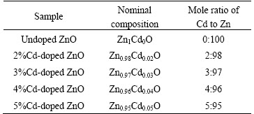
Zn1-xCdxO (x=0, 2, 3, 4 and 5, mass fraction, %) samples were synthesized by adding appropriate amount of Cd(CH3COO)2��2H2O to the Zn(CH3COO)2��2H2O) in the mixture of 50 mL distilled water and 50 mL ethanol. The molar ratio of Cd to Zn(Cd/(Zn+Cd)) was kept at about 0, 2%, 3%, 4%, and 5% for preparing undoped and Cd-doped ZnO samples, respectively. At the same time, 2 g of NaOH pellets were dropped into the 50 mL mixed solution of distilled water and ethanol. Thus, prepared NaOH solution was heated up to boiling temperature and the cadmium acetate dihydrate and zinc acetate dehydrate mixed solution were dropped slowly into the NaOH solution for 1 h and then cooled to room temperature (40 ��C). The solution turned into a milky white and the precipitation formed in the solution. 3 mL of polyethylene glycol (MW: 400) was added as capping agent. Following this, the precipitate was kept in an ultrasonic bath for 30 min and then allowed to settle down the particles for 7 d at room temperature. Then, the particles were repeatedly washed with ethanol to remove unwanted ions, and the obtained white precipitate was dried at 100 ��C overnight in a vacuum oven to get Cd-doped ZnO nanopowders. Finally, the powder samples were annealed at 750 ��C for 2 h. Details of the synthesized samples are given in Table 1.
2.2 Characterization
Crystal structure identification was performed using X-ray diffractometer (XRD: Philips Analytical Model No.-PW1830) equipped with Ni filtered Cu K�� radiation (��=1.54187  ) for 2��=10��-80��, with scanning rate of 1 (��)/min operated at 40 kV and 30 mA. Surface morphology and microstructure of the particles were studied by JEOL field emission scanning electron Microscope (JEOL FESM-6700: Japan) operated at 20 kV and 20 mA and the chemical composition was examined with energy-dispersive X-ray spectrometer (EDS: INCAPentaFET-x3, oxford instruments, UK). JEM-1010 transmission electron microscope (TEM) was used to study the microstructure and size of the nanoparticles. For TEM analysis the sample was ultrasonically dispersed in ethanol, and then a drop of a substance was placed on an amorphous carbon film supported by copper grid and dried in air. To identify the functional groups and to confirm the presence of Cd ions, the samples were examined with Fourier transform infrared spectrometer (FTIR; RX1 PERKINELMER: USA) at a resolution of 2 cm-1. The measurements were carried out in the region of 400-4000 cm-1 using KBr as the beam splitter. Optical absorption measurements in the UV-visible range were performed at room temperature using a Lambda 35 (PERKINELMER: USA) spectro- photometer. The wavelength range used in the experiment was 200 to 1100 nm. For this study, the powder samples were dispersed in de-ionized water and mixed well. Photoluminescence (PL) measurement was carried out using a PL spectrometer (Kimon, SPEC- 14031K, Japan) with a He-Cd laser line of 320 nm as the excitation source. A Renishaw micro-Raman spectrometer RM 2000 was employed to study the Raman spectra of the Zn0.95Cd0.05O sample under Ar+ ion laser (488 nm) excitation. Thermogravimetric analysis (TG) of Zn0.95Cd0.05O nanoparticles was performed on a Perkin-Elmer TGA7 at a heating rate of 10 ��C/min under nitrogen flow from room temperature (RT) to 1400 ��C. Differential scanning calorimetry (DSC) was performed on a NETZSCH DSC204 in nitrogen atmosphere at a heating rate of 10 ��C/min.
Table 1 Sample details
3 Results and discussion
3.1 Thermal analysis
Initially X-ray diffraction (XRD) patterns were recorded for the all the samples in the as-synthesized condition, as shown in Fig. 1. It can be seen that the samples with higher Cd content (>2%) consist of few additional peaks other than the characteristic peaks of ZnO. In order to decide the annealing temperature, TG and DSC analyses were performed for a 5%Cd-doped ZnO.
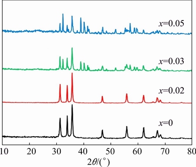
Fig. 1 XRD patterns of Zn1-xCdxO nanopowders in as-synthesized condition
Thermal analysis infers the phase change during crystallization. Figure 2 illustrates the combined TG and DSC plots of 5%Cd-doped ZnO nanoparticles at a heating rate of 10 ��C/min under nitrogen atmosphere from 50 to 1400 ��C. It is clear from the figure that there are three observable mass losses up to 800 ��C. The first mass loss of 4% occurs at 173 ��C (TG curve). The evaporation of residual hydrated acetate and other low molecular mass compounds could have caused the first mass loss. The second mass loss 1.12% has been detected at 423 ��C. This may be due to the decomposition of organic material and other volatile products. The third negligible mass loss has been recorded at around 650 ��C. This temperature is the onset temperature of crystallization. The residual mass recorded at 1400 ��C is 87.84%. This means that we observed only 12.16% mass change till 1400 ��C. Almost, the mass is constant even at higher temperature, indicating the oxide formation. Continuous trivial decrease in mass loss up to 1400 ��C confirms that the sample does not have measureable quantity of impurity phase like CdO.
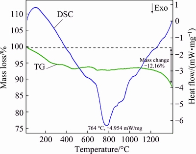
Fig. 2 Combined TG and DSC profile of 5% Cd doped ZnO sample
On the DSC curve, the endothermic peak found at 90 ��C is attributed to the evaporation of water [16]. Additionally, above 100 ��C, there is a smooth downward trend in DSC curve with significant mass loss. The observed hump at 550 ��C is believed to be the beginning of crystallization and the crystallization process finished at 764 ��C with a strong exothermic peak. Two more weak exothermic peaks around 950 ��C and 1100 ��C are the characteristic of thermal degradation through oxidation of organic residues. Therefore, TG and DSC analysis infers that the Cd-doped ZnO has good thermal stability at 800 ��C and the amount of Cd dopant in 5%Cd-doped ZnO is very little. Based on the crystallization temperature, Cd-doped samples were annealed at 750 ��C for 2 h and these annealed samples were used for the rest of the analyses.
3.2 Phase analysis
X-ray diffraction analysis is a powerful tool to estimate the lattice constant and average crystallite size, whether the samples possess single phase or multi-phase. XRD patterns of the annealed Zn1-xCdxO (x=0, 2%, 3%, 4% and 5% in mass fraction) nanoparticles are shown in Fig. 3. For all the samples the XRD peaks appearing at 31.8��, 33.4��, 36��, 47.5��, 56.5��, 62.8��, 66.3��, 67.9��, 69��, 72.6�� and 76.9�� correspond to the corresponding (100), (002), (101), (102), (110), (103), (200), (112), (201), (004) and (202) planes of the hexagonal wurtzite structure. All the diffraction peaks observed are in good agreement with standard diffraction data (JCPDS Card No.: 36-1451). Unfortunately, we have observed a very weak additional peak at 2��=38�� when the Cd content reaches 5%. It is suspected that it may be from the cubic CdO secondary phase. But in thermogravimetric analysis there is no signature for CdO secondary phase. In support of our result, ZHANG et al [17] have also reported ZnCdO quantum dots by sol-gel technique with secondary phases of Cd.
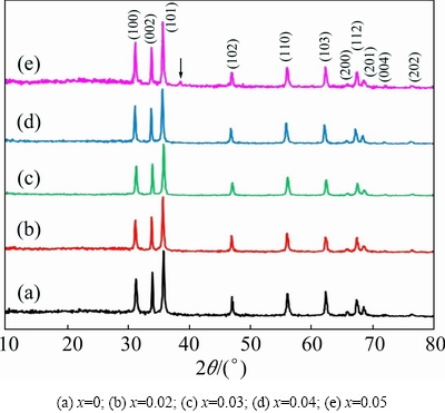
Fig. 3 XRD patterns of Zn1-xCdxO nanopowders after annealing at 750 ��C for 2 h
Average crystallite size (D) of the prepared nanoparticles has been calculated using a well known Debye-Scherrer formula [18] from the peak along the (101) plane.
 (1)
(1)
where �� is the wavelength of the X-ray used (1.54056 for Cu K�� radiation), �� is the full width at half maximum in radian (FWHM), and �� is the angle of diffraction. The average crystallite size is calculated to be 19.6 nm for ZnO and increases till 4% Cd. Thereafter, it decreases to 25.8 nm for 5% Cd. Our crystalline size calculation suggests that the solubility of Cd2+ ions in ZnO lattice is limited to 4%, and the excess doping tends to segregate on the surfaces of the nanocrystals. It also results in decreasing the crystallite size. It is remarkable that the solubility limit presented here is higher than those of the previous reports [4-6]. Moreover, the lattice constants a and c of synthesized samples were calculated using the following equation:
 (2)
(2)
where (hkl) are Miller indices, and d(hkl) is the interplanar distance of the particular plane obtained from the XRD analysis. Calculation shows that the average crystallite size increases with Cd dopant which clearly reveals the presence of Cd in the prepared samples. Then, the volume of the ZnO and ZnO:Cd unit cell has also been determined, according to the equation described below:
 (3)
(3)
The calculated values of crystalline size, lattice constants, and unit cell volume are listed in Table 2. Variations of crystalline size, lattice constants and unit cell volume with respect to Cd content are displayed in Fig. 4. It is observed that the intensity of the (002) peak decreases for 2% and 5% Cd. It reflects the deterioration in crystalline nature of the samples. It is also noticed that the position of the high intensity peak (101) in the Cd-doped ZnO samples shifts slightly towards the higher 2�� value. This shift rises due to the incorporation of a larger Cd2+ ion with ionic radius of 0.074 nm in place of Zn2+ ion with smaller ionic radius of 0.060 nm in the Zn1-xCdxO samples.
Table 2 Interplanar distance (d002), crystalline size, lattice parameter and unit cell volume of Zn1-xCdxO (x=0, 2, 3, 4, 5) nanoparticles
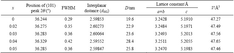
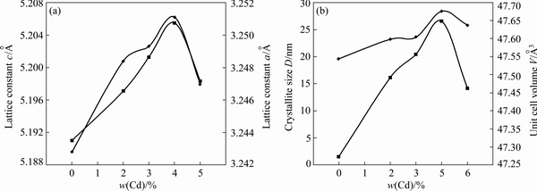
Fig. 4 Variation of lattice constant (a) and unit cell volume and grain size (b) vs Cd content of nanoparticles
3.3 UV-Vis spectra of Zn1-xCdxO nanoparticles
Optical absorption spectra of prepared Zn1-xCdxO nanoparticles recorded in the UV-Vis range of electromagnetic spectrum are displayed in Fig. 5. When the nanoparticle is exposed to UV-Vis radiation, the electrons in the outermost orbital of an atom (or) molecule absorb photons and undergo transition to higher energy levels. Therefore, the obtained absorption spectra can be used to calculate the energy gap of the undoped and Cd doped ZnO nanoparticles. The spectra show a distinct absorption band (��max ) at 360, 367, 378, 391 nm and then 387 nm corresponding to x=0.0, 0.02, 0.03, 0.04 and 0.05. The energy gap of the synthesized samples has been calculated according to the equation Eg=(1240/��max), where Eg is the energy gap and ��max is the wavelength of absorption by the synthesized nanoparticles. The estimated band gap values of the nanoparticles are found to be 3.44, 3.38, 3.28, 3.20 and 3.17 eV for x=0.0, 0.02, 0.03, 0.04 and 0.05, respectively. Calculation shows that Eg of 5%Cd-doped ZnO sample reported here is less than that of bulk ZnO reported in literatures. This reduction in Eg is owing to the presence of suspected CdO but it is not detected in TG and DSC analyses. The decrease in Eg is consistent with the previous report [17]
We then continued our investigation for the calculation of energy gap of nanoparticles with the familiar Tauc��s equation (��h��)2 =��(h��-Eg), where �� is the absorption coefficient, h�� is the energy of the photon and �� is a constant calculated from the refractive index and electron�Chole effective mass [19,20]. The dotted lines show the best fitted results. The extrapolation of the liner portion of the plot on the x-axis (h��) gives the Eg value. The energy gap value obtained thus decreases as 3.40, 3.37, 3.30, 3.21 and 3.15 eV for x=0, 0.02, 0.03, 0.04 and 0.05, respectively. Energy gap estimation based on the Tauc��s equation is illustrated in Fig. 6. Generally, doping may widen the energy gap of the semiconductor material with respect to the Burstein�CMoss effect [21]. But in our present study, Eg decreases with the boost in Cd doping, which can be attributed to the band gap renormalization because the Eg value of CdO is 2.3 eV, which is smaller than that (3.2 eV) of ZnO [22]. Hence, the formation of modest amount of CdO reduces the energy gap of 5%Cd-doped ZnO nanoparticles below 3.2 eV. Table 3 summarizes the Eg values obtained from UV-Vis spectrum and Tauc��s plot.
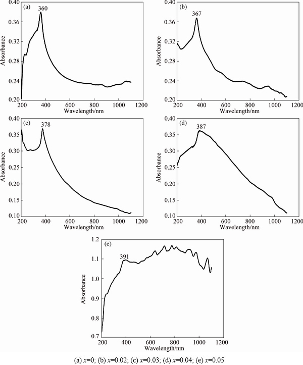
Fig. 5 UV-Vis absorption spectra of synthesized Zn1-xCdxO nanopowders
3.4 FTIR spectrum analysis
FTIR spectra of prepared ZnO:Cd nanostructure are shown in Fig. 7. They consist of series of absorption bands in the range between 400 and 4000 cm-1. The broad absorption band observed between 3412 and 3234 cm-1 is assigned to the O��H stretching mode for ��COOH group in zinc acetate and H2O molecule. The absorption band at 2723-2820 cm-1 corresponds to the C��H stretching vibrations of acetate. The bands appearing between 1359 and 1612 cm-1 are due to the symmetric and asymmetric stretching modes of the acetate group (��COOH), respectively. The absorption bands at 1035-1089 cm-1 are due to the C=O deformation mode. Remarkably, C=O deformation mode disappears completely due to the increase in Cd concentration above 4%. Rich Cd content may prevent the adsorption of C=O on the surface of the ZnO:Cd nanoparticles. Absorption bands observed around 850 and 714 cm-1 might be from C��OH group and O��H bending vibration (out-of-plane). The sharp bands positioned at 485 cm-1 are associated with the characteristic wurtzite lattice vibrations (Zn��O) and this stretching vibration is the indication of successful synthesis of ZnO [23], as previously confirmed by XRD. This wurtzite lattice vibration is disturbed as the Cd concentration attains 4%, therefore, the vibration becomes broader and it covers at 485-563 cm-1. This broadening is the result of Zn��Cd��O lattice vibration.

Fig. 6 Tauc��s plots for energy gap of Zn1-xCdxO nanopowders
Thus, the disappearance of the peak between 1036 and 1088 cm-1 in Cd-rich samples and the peak shifting from 485 cm-1 to 563 cm-1 confirm the substitution of heavier Cd2+ ions in the ZnO matrix. FTIR peak assignments are given in Table 4.
Table 3 Comparison of Eg values obtained from UV-Vis absorption spectrum and Tauc��s plot for Zn1-xCdxO
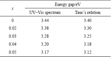
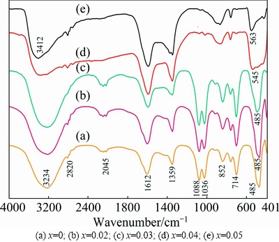
Fig. 7 FTIR spectra of synthesized Zn1-xCdxO nanopowders
3.5 PL spectra of synthesized nanopowders
We further studied the room temperature PL spectra of Cd-doped ZnO nanoparticles in the range of 350-600 nm at different Cd contents and the results are displayed in Fig. 8. All the prepared samples show six emission peaks. The first weak emission observed at 361 nm (3.43 eV) and the second strong emission observed at 391 nm (3.17 eV) belong to UV emission which is also known as near band edge (NBE) emission. NBE emission is the characteristic peak of ZnO. NBE is the result of recombination between the electrons in the conduction band and holes in the valence band [24]. Next to UV emission, the slightly less intense emission observed at 411 nm corresponds to the visible violet emission which indicates the high content of Zn vacancies. The blue emission centered at 444 nm is created by the defect levels created between the conduction band and valence band such as the shallow donor levels arising from Zn defects. However, some authors [25,26] claimed that this blue emission is originated from the Zn interstitial position. It is reported that OH- ions available on the surface of the ZnO are also a reason for this blue emission. The two green emissions seen at 492 and 521 nm are attributed to the native defects such as highly ionized oxygen vacancies.
Table 4 FTIR vibration frequencies of different modes of Zn1-xCdxO (x=0, 2, 3, 4, 5) nanocrystals
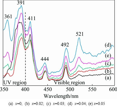
Fig. 8 Room temperature PL spectra of Zn1-xCdxO nanopowders
In PL spectrum, intensity of the visible emissions (defect related emission) is very weak compared with UV emission (NBE emissions), which implies that the samples have fewer defects. Here, we noticed the trend of concurrent increase in intensity of both UV and visible emission with minor change in position till x=0.04 (Fig. 8(d)). Further increase in x to 0.05 both UV and visible emissions decrease. The enhancement of the intensity shows that till 4% Cd doping, more number of defects are induced in the samples. As the Cd concentration is further increased to 5%, the intensity of both emissions immediately decreases. This is ascribed to the non-radiative energy transfer between lattice and defect states. Heavy Cd doping in ZnO nanoparticles may suppress the PL emission through the non-radiative recombination centers.
PL spectrum is also used to evaluate the crystalline quality of the synthesized nanoparticles from the ratio of intensity of UV to visible emission. If this ratio is large (>1) we can say that the synthesized nanoparticles have fewer defects and the crystals are highly pure. In the present study, the probable UV to visible ratios are 1.04 for undoped ZnO, 1.14 for 2%, 1.23 for 3%, and 1.24% for 4% and 5%Cd-doped ZnO samples. Regarding crystalline quality, it increases with Cd content. It is the good signature of the high quality of the synthesized nanopowders. Similar PL graph has already been reported by SONG et al [27].
3.6 FT-Raman spectra of Zn0.95Cd0.05O nanopowders
Space group of ZnO is  and it has two formula units per primitive cell with four atoms in each primitive cell [28]. Each Zn atom located at C3v sites (tetrahedrally coordinated to 4 O atoms and vice versa) leading to 12 phonon modes (9 optical and 3 acoustic modes). Thus, the Raman-active optical phonons zone-center is predicted by the group theory ��opt=A1+2B1+E1+2E2 [29]. Here, A1 and E1 modes are polar and split into transverse optical (TO) and longitudinal optical (LO) phonons whereas the B1 modes are Raman inactive [30]. E2 modes are non-polar but Raman active. These modes have two wave numbers classified as
  and
and  modes. mode is associated with the motion of O atom and with Zn sublattice. Therefore, the above optical phonon zone-center equation can be written as ��opt=A1+2E2+E1. Of these, A1 phonon vibrations are parallel to c-axis of the lattice so they are polarized parallel to the c-axis while E1 phonon vibrations are perpendicular to the c-axis of the lattice so perpendicularly polarized to the c-axis. Though all the modes correspond to a band with fixed wave number in the Raman spectrum, the intensities of these bands totally depend on the scattering cross-section. Strong mode is the characteristic peak of the wurtzite structure of ZnO lattice and it is a measure of good crystallinity of the lattice, while
  mode is due to the presence of oxygen vacancies and interstitial Zn ions.
To explore the effect of Cd doping on microscopic structure and vibrational properties, Raman scattering of the 5%Cd-doped ZnO nanoparticles was studied and the results are shown in Fig. 9. For our Zn0.95Cd0.05O nanoparticles, phonon scattering was observed at 261, 328, 389, 404, 437, 530, 564, 586 and 596 cm-1. The Raman peak at 261 cm�C1 could be assigned to 2E2 (low) mode, whereas the band located around 328 cm�C1 is assigned to - mode (multi-phonon scattering) of ZnO nanoparticles [31]. Less intense - band indicates the lattice distortion in the ZnO matrix by Cd doping, as seen from the grain size and lattice constant decrease in XRD study. Peak at 389 cm-1 corresponds to A1(TO) mode, whereas E1(TO) mode of vibration has been observed at 404 cm-1. The high frequency peak at 437 cm-1 is commonly attributed to the non-polar mode [32]. The broad nature of this strong Raman peak indicates that the wurtzite crystalline structure of ZnO might have been weakened by 5% Cd doping. The additional vibrational mode at 512 cm-1 should be ascribed to the local vibration related to the substitution of larger Cd2+ (ionic radius 0.074 nm) in place of smaller Zn2+ (0.060 nm). Raman peaks positioned at 530 and 564 cm-1 are assigned to longitudinal optical mode A1(LO) mode and the peaks positioned at 586 and 596 cm-1 are assigned to E1(LO) mode.
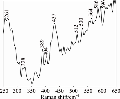
Fig. 9 FT-Raman spectrum of Zn0.95Cd0.05O nanopowder
3.7 FESEM, EDAX and TEM analysis
The surface morphology of the prepared nanopowders under different doping concentration has been performed by FESEM. Figures 10 shows the FESEM images of the Zn1-xCdxO nanopowders. As seen from the FESEM images, the nanoparticles of undoped ZnO nanoparticles are homogenous and non-agglomerated and the rough measurements of images show that the average size of particles varies between 18.8 and 28 nm without the presence of the other dominating phases. Also, the images show that the samples are free of any voids.
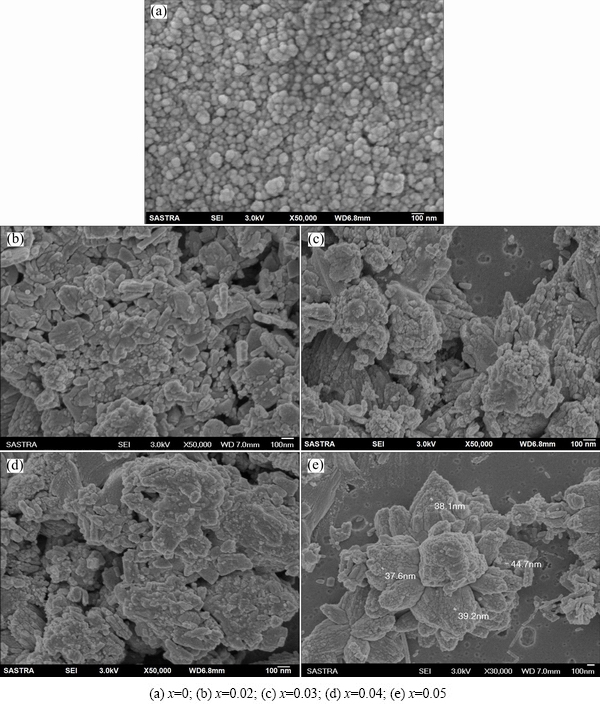
Fig. 10 FESEM images of synthesized Zn1-xCdxO nanopowders
The FESEM micrograph of the Cd-doped ZnO nanoparticles shows distinct, non-homogenous, and less agglomerated various nanostructures. Surprisingly, the microstructure is changed from spherical shape to mixed structure composed of nanoparticle, nanorods and nanoflakes as the Cd content increases. This mixed structure continues till 3% Cd. More amusingly, these mixed nanostructures arrange themselves to form a jasmine flower-like structure as the Cd content is increased to 5%. The image clearly reveals that this nanoflower has the particles of thickness below 50 nm and grows upward to form 3D jasmine flower-like morphology. Still there are few isolated nanoneedles of 100 nm-1 ��m in size, even after forming the flower-like structure. In addition, we do not see any secondary phase of Cd at the grain boundaries even the Cd content is 5%. To the best of our knowledge, 5% is the maximum Cd content that can be doped with ZnO using a simple chemical precipitation method without any secondary phases. It is well known that nanoparticles are sensitive to synthesis method and reaction temperature. It is believed that 7 d of aging at room temperature (40 ��C) and the 5% Cd may be the reason for the formation of flower-like structure and effective doping.
To authenticate the existence of dopant on ZnO, EDAX analysis was carried out. The EDAX is a chemical microanalysis technique used together with FESEM. Typical EDAX images of the undoped and 2%Cd-doped ZnO samples are illustrated in Fig. 11. Table 5 represents the Zn, Cd and O contents obtained from EDAX measurements. From the EDAX images, it can be seen that Cd contents on the samples are in good conformity with the nominal and observed values. It is valuable to note that the synthesized nanoparticles are mainly composed of Zn, Cd and O.
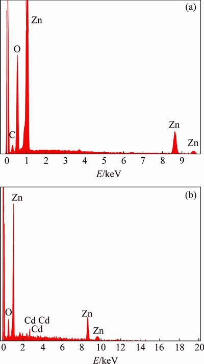
Fig. 11 EDAX analysis of ZnO (a) and Zn0.98Cd0.02O (b) nanopowders
Table 5 Results of Zn1-xCdxO composition analysis (mass fraction, %)
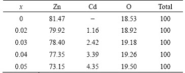
In order to get direct information about the particle size and morphology of the synthesized nanocrystalline samples, transmission electron micrograph analyses were made. Representative TEM image of 5%Cd-doped ZnO sample and its corresponding selected area diffraction pattern (SAED) and fringe width patterns are shown in Figs. 12(a)-(c), respectively. From Fig. 12(a), it can be seen that the sample contains particles of uniform size. The calculated average particle size from TEM analysis is 20-40 nm, which matches well with the same obtained from optical studies and XRD analysis. The SAED pattern indicates that the particles are single crystalline in nature and are free of major lattice defects. The fringe pattern with plane distance of 0.264 nm corresponds to (002) plane of 5%Cd-doped ZnO sample. This interplanar distance is in line with the XRD data of the sample concerned, which is slightly greater than the interplanar distance of the (002) plane of undoped ZnO (0.260 nm). Therefore, the SAED pattern of 5%Cd-doped ZnO sample confirms the Cd dopant and also confirms the single crystalline nature of 5%Cd-doped ZnO nanoparticles.
4 Conclusions
Cd-doped ZnO (Zn1�CxCdxO, x=0-0.05) semi- conductor nanoparticles were prepared successfully by the simple chemical precipitation method. XRD analysis confirms that the grain size increases up to 4% Cd dopant and the further increase in Cd content decreases the grain size. UV-Vis absorption spectra show that the red shift in absorption from 360 to 391 nm until the Cd content reaches 5%. The corresponding energy gap decreases from 3.44 to 3.17 eV. Tauc��s relation also confirms the decrease in energy gap. FTIR analysis also confirms the Cd dopant through the peak shifting from 485 to 563 cm-1. Photoluminescence spectra of the synthesized nanopowders confirm that Cd dopant enhances the emission property, particularly green emission till 4%. The broad and high frequency Raman peak at 437 cm-1 indicates that the wurtzite crystalline structure of ZnO is weakened by 5% Cd doping. FESEM images confirm the microstructural transformation from nanoparticle to jasmine flower-like microstructure on 5% Cd dopant, as the case of UV analysis. Microstructural transformation from nanoparticle to jasmine flower-like microstructure is the novelty of the present work. Finally, it is concluded that the data presented here confirm that Cd can be doped in ZnO lattice till up to 5% by chemical precipitation method.
Fig. 12 Typical TEM image (a), corresponding SAED pattern (b), and its fringe width pattern (c) of 5%Cd-doped ZnO sample
Acknowledgments
Authors thank SAIF IIT(M) for providing TG and DSC analyses and STIC-Cochin for providing TEM experimental facilities to carry out the present work. One of the author R. SANTHI would like to thank the Research scholars M. Jay CHITHRA, C. THANGAMANI and M. PONNAR of Nanomaterials Research Laboratory, Department of Physics, Government Arts College, Karur, for their timely help in the long process of sample preparation.
References
[1] PUSHPANATHAN K, SATHYA S, JAY CHITHRA M, GOWTHAMI S, SANTHI R. Influence of reaction temperature on crystal structure and band gap of ZnO nanoparticles [J]. Materials and Manufacturing Processes, 2012, 27: 1334-1342.
[2] JAY CHITHRA M, SATHYA M, PUSHPANATHAN K. Effect of pH on crystal size and photoluminescence property of ZnO nanoparticles prepared by chemical precipitation method [J]. Acta Metallurgica Sinica (English Letters), 2015, 28(3): 394-404.
[3] WAN Q, LI Q H, CHEN Y J, WANG T H, HE X L, GAO X G, LI J P. Positive temperature coefficient resistance and humidity sensing properties of Cd-doped ZnO nanowires [J]. Applied Physics Letters, 2004, 84: 3085-3087.
[4] SAMUEL T, ESUB BASHA S K, YUGALA E, DAMODARASATISH K, SURESH J, INDUMATI KRISHNAVENI K, SPANDANA KJMS, SUBBARAO D, RAMACHANDRA RAO K. Structural, optical and photoluminescence studies on Cd-doped ZnO nanoparticles: Synthesized by polyol method [J]. International Journal of Scientific Research, 2014, 32:116-118.
[5] NARAYAN A, MISHRA M K. Effects of Cd doping on structural, optical and photoconductive properties of ZnO nanoparticles [EB/OL]. International Journal of Science and Research, 2012: 1558-1562.
[6] RANA N, SUBHASH CHAND, GATHANIAN A K. Tailoring the structural and optical properties of ZnO by doping with Cd [J]. Ceramics International, 2015, 41: 12032-12037.
[7] SHIGEMORI S, NAKAMURA A, ISHIHARA J, AOKI T, TEMMYO J. Zn1-xCdxO film growth using remote plasma-enhanced metal organic chemical vapour deposition [J]. Japanese Journal of Applied Physics, 2004, 43(43): L1088-L1090.
[8] MAKINO T, SEGAWA Y, KAWASAKI M, OHTOMO A, SHIROKI R, TAMURA K, YASUDA T, KOINUMA H. Band gap engineering based onMgxZn1-xOandCdyZn1-yOternary alloy films [J]. Applied Physics Letters, 2001, 78: 1237-1239.
[9] GHOSH M, RAYCHAUDHURI A K. Structure and optical properties of Cd-substituted ZnO (Zn1-xCdxO) nanostructures synthesized by the high-pressure solution route [J]. Nanotechnology, 2007, 18(11): 4473-4476.
[10] VIJAYLAXMI S, VENKATRAJ S, JAYAVEL R. Characterization of cadmium doped zinc oxide (Cd:ZnO) thin films prepared by spray pyrolysis method [J]. Journal of Physics D:Applied Physics,2008, 41: 245403.
[11] VIDYASAGAR C C, ARTHOBA NAIK Y, VISWANATHA R, VENKATESH T G. Optical properties of dye-sensitized films based on Cd-ZnO nanoparticles [J]. Nanoscience and Nanotechnology: An International Journal, 2012, 2: 18-23.
[12] ALI FATIMA A, SUGANTHI D. The influence of dopants (Cd and Al) on the physical properties of ZnO [J]. International Journal of Engineering Science and Research, 2011, 2: 1-10.
[13] WANG F Z, YE Z Z, MA D W, ZHU L P, ZHUGE F, HE H P. Synthesis and characterization of quasi-aligned ZnCdO nanorods [J]. Applied Physics Letter, 2005, 87(14): 5584.
[14] WANG Y, YANG Y, ZHANG X, LIU X, NAKAMURA A. Optical investigation on cadmium-doped zinc oxide nanoparticles synthesized by using a sonochemical method [J]. Crystengcomm, 2012, 14(1): 240-245.
[15] JAY CHITHRA M, PUSHPANATHAN K, LOGANATHAN M. Structural and optical properties of Co-doped ZnO nanoparticles synthesized by precipitation method [J]. Materials and Manufacturing Processes, 2014, 29: 771-779.
[16] WONG E W, MAYNOR B W, BURNS L D , LIEBER C M. Growth of metal carbide nanotubes and nanorods [J]. Chemistry of Materials, 1996, 8: 2041-2046.
[17] ZHANG J, ZHAO S Q, ZHANG K, ZHOU J Q, CAI Y F. A study of photoluminescence properties and performance improvement of Cd-doped ZnO quantum dots prepared by the sol�Cgel method [J]. Nanoscale Research Letters, 2012, 7: 405.
[18] CULLITY B D. Elements of X-ray diffraction [M]. 2nd ed. MA, USA: Addison-Wesley Publishing Co., Inc., 1978: 102.
[19] WILLIAMSON G B, SMALLMAN R C. Dislocation densities in some annealed and cold-worked metals from measurements on the X-ray Debye-Scherrer spectrum [J]. Philosophical Magazine, 1956, 1: 34-46.
[20] TAUC J, MENTHE A. States in gap [J]. Journal ofNon-Crystalline Solids, 1972, 8: 569-585.
[21] PANKOVE J I. Optical process in semiconductors [M]. NJ: Prentice�CHall, Englewood Cliffs, 1971.
[22] BANERJEE P, LEE W J, BAE K R, LEE S B, RUBLOFF G W. Structural, electrical, and optical properties of atomic layer deposition Al-doped ZnO films [J]. Journal of Applied Physics, 2010,108: 043504.
[23] MAITI U N, GHOSH P K, AHMED S F, MITRA M K, CHATTOPADHYAY K K, Structural, optical and photoelectron spectroscopic studies of Nano/Micro ZnO:Cd rods synthesized via sol-gel route [J]. Journal of Sol-Gel Science and Technology, 2007, 41: 87-92.
[24] ZHAO B, ZHAO S, ZHANG K, LIU D, SU J. Preparation and characterization of thiourea modified water soluble Cd doped ZnO quantum dots [J]. Acta Chimica Sinica, 2011, 69: 777-782.
[25] WANG F Z, HE H P, YE Z Z, ZHU L P. Photoluminescence properties of quasialigned ZnCdO nanorods [J]. Journal of Applied Physics, 2005, 98: 084301-084304.
[26] GHOSH M, RAYCHAUDHURI A K. Structural and optical properties of Zn1-xMgxO nanocrystals obtained by low temperature method [J]. Journal of Applied Physics, 2006, 100: 034315.
[27] REYNOLDS D C, LOOK D C, JOGAI B. Fine structure on the green band in ZnO [J]. Journal of Applied Physics, 2001, 89: 6189-6191.
[28] SONG J L, ZHENG J H, ZHAO Z, ZHOU B Y, LIAN J S. Synthesis and Photoluminescence of Y and Cd doped ZnO nanopowder [J]. Transactions of Nonferrous Metals Society of China, 2013, 23: 2336-2340.
[29] BRAGG W L. The arrangement of atoms in crystal [J]. Philosophical Magazine, 1920, 40: 169-189.
[30] FATELY W G, MCDEVITT N T, BENNTLEY F F. Infrared and Raman selection rules for lattice vibrations-the correlation method [J]. Applied Spectroscopy, 1971, 25: 155-173.
[31] DAMEN T C, PORTO S P S, TELL B. Raman effect in zinc oxide [J]. Physical Review, 1966, 142: 570-574.
[32] MANJON F J, SYASSEN K, LAUCK R. Effect of pressure on phonon modes in wurtzite zinc oxide [J]. High Pressure Research, 2002, 22: 299-304.
Zn1-xCdxO�������е�����װ��״�ṹ
R. SANTHI1,2, C. SHANTHI2, M. SATHYA3, K. PUSHPANATHAN3
1. Department of Physics, Mahendra Institute of Engineering and Technology, Namakkal 637503, India;
2. Department of Physics, Sona College of Technology, Salem 636005, India;
3. Nanomaterials Research Laboratory, Department of Physics, Government Arts College, Karur 639005, India
ժ Ҫ���о��������ϳ�Cd����ZnO�������Ľṹ��ѧ������X���������������������Cd���û���Ӱ��ZnO�Ļ���Ǧп���ͽṹ������Cd����������4%��ƽ�������ߴ硢��������͵���������ӡ���������ɼ����չ���Tauc���ⶨ��Ʒ����϶����϶��Cd�������Ӷ���С������Ҷ�任�������ͨ��485~563 cm-1��ȷ��Cd��������·�����ǿ������Ҳȷ����Cd�����437 cm-1���Ŀ������������5%��Cd����������ZnO��Ǧп���ͽṹ��������ɨ��羵����Ҳ֤ʵ�����׳ߴ����ӵĴ��ڣ���֤���˲���5% Cdʱ�ṹ��������ת��ɻ�״�ṹ��
�ؼ��ʣ�Cd���ӣ�ZnO����������϶������ṹ������֯�����·���
(Edited by Xiang-qun LI)
Corresponding author: R. SANTHI; Tel: +91-9842546669; Fax: +91-4324222931; E-mail: santhimec@gmail.com
DOI: 10.1016/S1003-6326(17)60228-0
Abstract: The structural and optical characterization of cadmium-doped zinc oxide nanoparticles synthesized by precipitation method was studied. X-ray diffraction study confirmed the substitution of cadmium dopant without disturbing the basic wurtzite structure of zinc oxide. The average crystalline size, lattice constants and unit cell volume also increased up to 4% of cadmium doping. Energy gaps of the samples were determined from the ultraviolet-visible absorption spectrum as well as Tauc��s plot which infers that the energy gap decreases with the increase of cadmium content. Fourier transformation infrared spectrum confirms the cadmium dopant through peak shifting from 485 to 563 cm-1. Photoluminescence spectrum also defines the cadmium dopant by intensity increase. The broad Raman peak at 437 cm-1 indicates that the wurtzite structure of zinc oxide is weakened by 5% cadmium doping. Field emission scanning electron microscope study also confirms the existence of particles in nanometer size and it indentifies the microstructure transformation from nanoparticles to jasmine flower-like structure on 5% cadmium doping.
