

Structure and electronic properties of SiC thin-films deposited by RF magnetron sputtering
ZHOU Ji-cheng(�ܼ̳�), ZHENG Xu-qiang(֣��ǿ)
School of Physics Science and Technology, Central South University, Changsha 410083, China
Received 28 July 2006; accepted 25 October 2006
Abstract:
SiC thin-films were prepared by RF-magnetron sputtering technique(RMS) with the target of single crystalline SiC and then annealed. The surface morphology of thin-films was characterized by AFM. The result shows that the surface of the thin-films is smooth and compact; XRD analysis reveals that the thin-films are amorphous. The thickness, square-resistance and curves of resistance��temperature were measured. The results show that the curves of lnR versus 1/kT both before and after annealing satisfy the expression of lnR��?W/kT, where ?W is electron excitation energy in the range of 0.014 2-0.018 5 eV, and it has a trend of increasing when the temperature is increased. After synthetical analysis we get the conclusion that the electronic mechanism of the thin-films is short distance transition between the localized states in the temperature range of 25-250 ��. The resistivity is in the range of 2.4��10-3-4.4��10-3 ��?cm and it has the same trend as electron excitation energy when annealing temperature is increased, which further confirms the electronic mechanism of thin-films and the trend of electron excitation energy versus annealing temperature.
Key words:
amorphous SiC thin-films; surface morphology; electron excitation energy; resistivity;
1 Introduction
Silicon carbide(SiC) is a promising semiconductor material because of its excellent physical and chemical properties, such as the wide band gap, large electrical breakdown field, high thermal electronic conductivity, high saturated electron velocity, large resistance to radialization and high surface hardness. These properties make SiC suitable for high frequency, high power, high temperature applications, source of blue light[1-2], as well as corrosion-resistant coating[3]. However, for single crystal SiC, the growth of these layers is generally achieved at substrate temperatures higher than 1 200 ��[4], but this elevated temperature would generate a high density of voids and a high concentration of defects at the interface. Such effects can be significantly avoided when growing polycrystalline or amorphous layers at lower temperatures, which has characteristics suitable for applications in microelectronic and optoelectronic devices such as light emitting diodes, phototransistors[5], solar cells[6] and temperature sensors[7].
Thus the development of low temperature processes to prepare SiC thin-films is essential for the practical application of SiC. Some methods of deposition are used, for instance, plasma enhanced chemical vapor deposition (PECVD)[8], laser-assisted deposition[9], and magnetron sputtering[10]. From these, magnetron sputtering process appears to be very attractive due to its low cost, high deposition rates, low deposition temperature, good adhesion and so on[11].
In this study, SiC thin-films were prepared by RF-magnetron sputtering technique(RMS) and the structure and electrical properties of the thin-films were mainly discussed.
2 Experimental
SiC thin-films were obtained in a RF (13.56 MHz) magnetron sputtering apparatus using a sintered SiC target (99.9% purity) of 100 mm in diameter and 5 mm in thickness. High purity argon (99.99%) was used as sputtering gas and polished glass was used as substrate material. Prior to each film deposition, the substrates by cleaning with acetone and alcohol in an ultrasonic bath for 15 min, respectively, and then rinsed with deionized water again. The sputtering was performed with an Ar pressure of 1.5 Pa and RF power of 150 W in the chamber evacuated to 1��10-3 Pa before argon gas was introduced in a flow of 150 mL/min through a mass flow controller. Thin-films were deposited at room temperature and the deposition time was 25 min. Before each deposition, a 10 min pre-sputtering was performed in order to remove the native oxide layer formed on the target surface. After this pre-sputtering stage, the shutter covering the substrates was removed and deposition initiated. After deposition, the samples were submitted to anneal using CS101-EBN type furnace at 200 �� and 300 �� for 20 min, respectively.
The morphology of the thin-films was analyzed by NT-MDT type atomic force microscopy(AFM). The structure of the films was examined by X-ray diffraction(XRD) with Cu K�� radiation in a standard X-ray diffractometer. The thickness was measured by Alpha-StepIQ type profiler. The curves of resistance�� temperature were measured by furnace of CS101-EBN and 71/2 Digit Nano Volt/Micro ohm Meter of 34420A in the temperature range of 25-250 ��. And the square- resistance was measured by Four-Point Probe of SDY-4D type.
3 Results and discussion
3.1 AFM characterization
The AFM images of as-deposited and annealed SiC thin-films are shown in Figs.1 and 2. From the images we can learn that the thin-films grow in a way of columns or gains and the surface is very compact. The gains are uniform and small, and they are all in the shape of ellipse, which is consistent with Refs.[12-13]. After annealing the gains grow larger and the roughness turns to 4.878 nm from 3.469 nm.
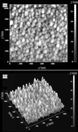
Fig.1 AFM images of deposited SiC thin-films
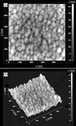
Fig.2 AFM images of SiC thin-films annealed at 200 ��
3.2 XRD analysis
XRD patterns show that the thin-films deposited and annealed at different temperatures are all amorphous with the RF power of 150 W at the pressure of 1.5 Pa, which is consistent with Refs.[14-15]. Fig.3 shows one of the XRD patterns of thin-films annealed at 300 ��. Obviously no SiC diffraction peaks can be found, which is because of the low substrate temperature and low annealing temperature.
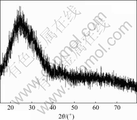
Fig.3 XRD pattern of thin-films annealed at 300 �� given by
3.3 Relationship of resistance versus temperature
The thin-films are amorphous SiC, which has been confirmed by XRD patterns and AFM images. Referred to the theory of semiconductor physics[16], the electronic conductivity of amorphous semiconductor is
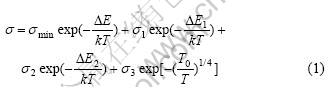
where the first term is responsible for the electric conductivity of extended states, ��min=quNc, ?E=Ec-EF; the second term is responsible for the electric conductivity of band tail states at low temperature, ?E1=EA-EF+?W1, and ?W1 is the average energy between localized states of band tail; the third term is responsible for the electric conductivity of short distance transition at lower temperature, ?E2=2��rkT+?W2, and ?W2 is the average electron excitation energy of phone-assistant transition between localized states; the forth term is the electric conductivity of transformable distance transition at very low temperature (about 10 T).
For amorphous semiconductors, the different electric-conducting mechanism plays dominating role at different ranges of temperature[16]. Referring to the theory mentioned above, we can get the same expression of resistivity R versus temperature T at different temperature ranges except for very low temperature of about 10 T:
![]()
From Eqn.(2), we can learn that lnR is linear with 1/kT and the slope is ?W. The curves of lnR versus 1/kT of the thin-films are shown in Fig.4.
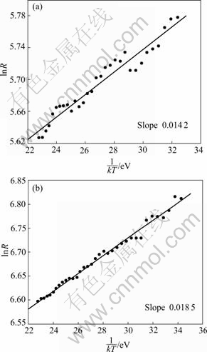
Fig.4 Curves of lnR versus 1/kT: (a) As-deposited film; (b) Film annealed at 300 ��
It can be seen that the relationship of resistance versus temperature of both deposited and annealed films satisfies the Eqn.(2), which proves that the thin-films are semiconductor. And then ?W can be got by the slope of the fitted line using the method of least squares. It is obvious that the thin-films annealed at 300 �� fit Eqn.(2) much better than the thin-films before annealing. That is because the annealing processes make the thin-films much more stable[17].
3.4 Discussion of electric-conducting mechanism
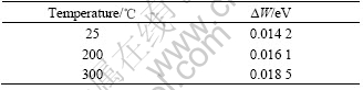
Table 1 lists the ?W at different annealing temperatures. It is easy to find that the magnitude of all ?W is 10-2 eV. However, the band gap of amorphous SiC is from 1.6 eV to 2.86 eV[18-19] and both of ?E and ?E1 corresponding to electric conductivity of extended states and band tail states have the same magnitude as band gap, which means the electric-conducting mechanism is different. Also the transformable distance transition is at very low temperature of about 10 T, so we deduce that the electric-conducting mechanism of thin-films is short distance transition between the localized states and ?W is right the average electron excitation energy of phone-assistant transition between localized states. Again, the average energy of electron excitation energy between localized states is at the magnitude of 10-2 eV that is consistent very well with our experimental results from 0.014 2 eV to 0.018 5 eV, and this gives a great support to the electric-conducting mechanism deduced in this study.
Table 1 ?W values at different temperatures
3.5 Thermal annealing effect on electron excitation energy
Thermal annealing is a very important technique for thin-films preparing process. It can make the thin-films much more stable through decreasing free energy. The curves of electron excitation energy versus annealing temperature are presented in Fig.5.
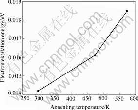
Fig.5 Electron excitation energy of thin-films as function of annealing temperature
It can be seen that the electron excitation energy has a trend of increasing as the annealing temperature increases. There is the explanation when the annealing temperature is increased, the expression W/B increases where W is the energy wide between centre energy E0 and edge energy En, and B is the band gap. That means the ruleless potential becomes stronger. So the electron excitation energy of phone-assistant transition between localized states becomes larger[20].
3.6 Effect on resistivity of thermal annealing
In order to probe into the thermal annealing effect on resistivity, the square-resistance of thin-films is measured. Combined by the thickness of thin-films, the resistivity is calculated whose range is from 2.4��10-3 to 4.4��10-3 ��?cm. Fig.6 shows the resistivity of SiC thin- films at varied annealing temperatures.
It is easy to find that the resistivity is increased when annealing temperature is increased and it has the same trend as electron excitation energy versus annealing temperature. Based on the electric-conducting mechanism of thin-films discussed before, the relationship of electron excitation energy and resistivity satisfies the following expression:
�ѡ�exp(?W/kT) (3)
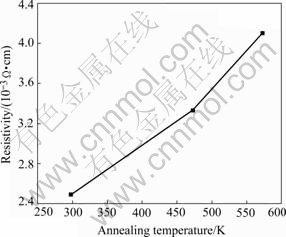
Fig.6 Resistance variety of thin-films versus annealing temperature
However, in this study the electron excitation energy is calculated through Eqn.(2) using data measured in the experiment, while the resistivity is calculated by the square-resistance and thickness of the SiC thin-films, which means that the results using two different methods are coincident. This further confirms the electric- conducting mechanism and the trend of electron excitation energy versus annealing temperature of thin- films.
4 Conclusions
1) Amorphous SiC thin-films were grown by RF- magnetron sputtering at the RF-power of 150 W and the gas pressure of 1.5 Pa. From the AFM images we can learn that the thin-films grow in a way of columns or gains and are very compact. The gains are uniform, small and of ellipse shapes. XRD analysis reveals that the thin-films are amorphous.
2) The curves of lnR versus 1/kT both before and after annealing satisfy the expression of lnR��?W/kT. The electron excitation energy of SiC thin-films is from 0.014 2 eV to 0.018 5 eV and it has a trend of increasing when the annealing temperature is increased. Considering all the above factors, we can deduce that the electric-conducting mechanism is short distance transition between the localized states. The resistivity of SiC thin-films is in the range of 2.4��10-3-4.4��10-3 ��?cm and it has the same trend as electron excitation energy when the annealing temperature is increased, which further confirms the electric-conducting mechanism of thin-films and the trend of electron excitation energy versus annealing temperature.
References
[1] LEI Y M, YU Y H, REN C X, ZOU S C, CHEN D H, WONG S P, WILSON I H. Compositional and structural studies of DC magnetron sputtered SiC films on Si(111) [J]. Thin Solid Films, 2000, 365: 53-57.
[2] SHA Z D, WU X M, ZHUGE L J. Structure and photoluminescence properties of SiC films synthesized by the RF-magnetron sputtering technique [J]. Vacuum, 2005, 79: 250-254.
[3] YAO Wang, ZHANG Yu-min, HAN Jie-cai, ZUO Hong-bo. Fabrication and test of reaction bond silicon carbide for optical applications [J]. Trans Nonferrous Met Soc China, 2006, 16: 409-413.
[4] KERDILES S, RIZK R, PEREZ-RODRIGUEZ A, GARRIDO B, GONZ?LEZ-VARONA L, CALVO-BANIO, MORANTE J R. Magnetron sputtering synthesis of silicon-carbon films: Structural and optical characterization [J]. Solid-State Electronics, 1998, 42(12): 2315-2320.
[5] SCHMIDT H, FOTSING E R, BORCHARDT G, CHASSAGNON R, CHEVALIER S, BRUNS U. Crystallization kinetics of amorphous SiC films: Influence of substrate [J]. Applied Surface Science, 2005, 252: 1460-1470.
[6] STAMATE M D. Strong dependence of IR absorption in ��-SiC?H dc magnetron sputtered thin films on H2 partial pressure [J]. Applied Surface Science, 2001, 172: 47-50.
[7] WANG Yin-yue, WANG Hui-yao, MA Guo-bin. Effects of high-temperature annealing on the structure of reactive sputtering ��-SiC?H films [J]. Thin Solid Films, 1998, 335: 249-252.
[8] GIORGIS F, PIRRI C F, TRESSO E, RAVA P. ��-SiC?H films deposited by PECVD from silane+acetylene and silane+acetylene+hydrogen gas mixture [J]. Diamond and Related Materials,1997, 6:1606-1611.
[9] MUTO H, KAMIYAB S, KUSUMORI T. Growth mechanism of ��-SiC hetero-epitaxial films by PLD as studied on the laser photon, pulse-width and substrates dependence [J]. Optical Materials, 2003, 23: 43-47.
[10] TANG Hui-dong, TAN Shou-hong, HUANG Zheng-ren, DONG Shao-ming, JIANG Dong-liang. Surface morphology of ��-SiC coatings deposited by RF magnetron sputtering [J]. Surface & Coatings Technology, 2005, 197: 161-167.
[11] RAJAB S M, OLIVEIRA I C, MASSI M, MACIEL H S, DOS SANTOS FILHO S G, MANSANO R D. Effect of the thermal annealing on the electrical and physical properties of SiC thin films produced by RF magnetron sputtering [J]. Thin Solid Films, 2006, 515: 170-175.
[12] ZHAO Wu, ZHANG Zhi-yong, WU Tie-zhu, WANG Xue-wen, DENG Zhou-hu, DAI Kun. The preparation of SiC films and study of ambience response [J]. Electron Device and Material, 2005, 24(9): 36-41.
[13] SIMAO R A, COSTA A K, ACHETE C A, CAMARGO JR S S. Magnetron sputtering SiC films investigated by AFM [J]. Thin Solid Films, 2000, 377/388: 490-494.
[14] AN Xia, ZHUANG Hui-zhao, LI Huai-xiang, XUE Cheng-shang. The annealing effect in H2 of SiC films by magnetron sputtering on Si(111) [J]. Chinese Journal of Semiconductors, 2002, 23(6): 593-597. (in Chinese)
[15] XIE Er-qing, ZHANG Zhi-min, MA Zi-wei. Epitaxial growth of ��-SiC by RF sputtering on silicon substrates and its porosity by electrochemical anodization [J]. Optical Material, 2003, 23: 157-161.
[16] LIU En-ke, ZHU Bing-sheng, LUO Jin-sheng. Physics of Semiconductor [M]. Xi��an: Xi��an Jiaotong University Press, 1998.
[17] SHA Z D, WU X M, ZHUGE L J. The structure and photo luminescence properties of SiC films doped with Al [J]. Physics Letters A, 2005, 346: 186-192.
[18] DANG JI-ping. Recent development of high temperature semiconductor device [J]. Semiconductor Information, 1994, 31(2): 46-56.
[19] XU Jun, YANG Ling, RUI Yun-jun, MEI Jia-xin, ZHANG Xin, LI Wei, MA Zhong-yuan, XU Ling, HUANG Xin-fan, CHEN Kun-ji. Photoluminescence characteristics from amorphous SiC thin films with various structures deposited at low temperature [J]. Solid State Communications, 2005, 133: 565-568.
[20] HE Yu-liang, CHEN Guang-hua, ZHANG Fang-qing. Physics of Amorphous Semiconductor [M]. Beijing: Higher Education Press, 1989. (in Chinese)
Foundation item: Project(60371046) supported by the National Natural Science Foundation of China
Corresponding author: ZHOU Ji-cheng; Tel: +86-731-8836381; E-mail: jicheng@mail.csu.edu.cn
Abstract: SiC thin-films were prepared by RF-magnetron sputtering technique(RMS) with the target of single crystalline SiC and then annealed. The surface morphology of thin-films was characterized by AFM. The result shows that the surface of the thin-films is smooth and compact; XRD analysis reveals that the thin-films are amorphous. The thickness, square-resistance and curves of resistance��temperature were measured. The results show that the curves of lnR versus 1/kT both before and after annealing satisfy the expression of lnR��?W/kT, where ?W is electron excitation energy in the range of 0.014 2-0.018 5 eV, and it has a trend of increasing when the temperature is increased. After synthetical analysis we get the conclusion that the electronic mechanism of the thin-films is short distance transition between the localized states in the temperature range of 25-250 ��. The resistivity is in the range of 2.4��10-3-4.4��10-3 ��?cm and it has the same trend as electron excitation energy when annealing temperature is increased, which further confirms the electronic mechanism of thin-films and the trend of electron excitation energy versus annealing temperature.
