
Article ID: 1003-6326(2005)05-0978-07
Improvement of wear resistance of AZ31 and AZ91HP by high current pulsed electron beam treatment
GAO Bo(�� ��)1, 2, HAO Sheng-zhi(��ʤ��)2,
DONG Chuang(�� ��)2, TU Gan-feng(Ϳ�ӷ�)1
(1. School of Materials and Metallurgy, Northeastern University, Shenyang 110004, China;
2. State Key Laboratory for Materials Modification by Laser, Ion and Electron Beams,
Department of Material Science and Engineering, Dalian University of Technology, Dalian 116024, China)
Abstract:
The surface modification of magnesium alloys (AZ31 and AZ91HP) was studied by a high current pulsed electron beam(HCPEB). The results show that the cross-sectional microhardness of treated samples increases not only in the heat affected zone(HAZ), but also beyond HAZ, reaching over 250��m. This is due to the action of quasi-static thermal stress and the shock thermal stress wave with materials, which result in its fast deformation on the surface layer and so increases microhardness. For the AZ91HP alloy, a nearly complete dissolution of the intermetallic phase Mg17Al12 is observed, and a super-saturated solid solution forms on the re-melted surface, which is due to the solute trapping effect during the fast solidification process. Measurements on sliding wear show that wear resistance is improved by approximately 5.6 and 2.4 times for the AZ31 and AZ91HP respectively, as compared with as-received samples.
Key words:
magnesium alloys; wear; high current pulsed electron beam(HCPEB) CLC number: TG166.3;
Document code: A
1 INTRODUCTION
Magnesium alloys, which have some essential advantages, such as lower density and higher strength, intend to take the place of conventional metallic materials, and have consequently found their applications in air, automobile and electron industry[1-2]. But the poor resistance to wear and corrosion is serious impediment against wider application of magnesium alloys. Considering that wear and corrosion are both related to the surface properties of magnesium alloys, it is important and necessary to find effective surface modification method to improve their corrosion and wear resistance.
Recently, the application of energetic beams such as ion, electron, laser and plasma is of increasing interest to surface modification of metallic materials. Among them, high current pulsed electron beam(HCPEB) is a relatively new technique[3-9]. The main feature of the pulsed electron systems is the high power density of 109-1012W/cm2 on the target surface. Irradiation induces dynamic temperature fields on the surface layers giving rise to superfast heating, melting and evaporation, followed by superfast solidification of the material[10-15]. The dynamic stress fields formed cause intense deformation processes in the material. As a result, metastable structure-phase states may appear on the surface layers, which are capable of providing improved physical, chemical and strength properties of the material unattainable with conventional surface treatment techniques.
In our previous work, it was found that HCPEB treatment is an effective method to improve wear resistance of metallic materials, for example, the friction and wear resistance of D2 die steel and H13 steel are significantly increased after HCPEB treatment[16-17]. In the present study, high current pulsed electron beam(HCPEB) was used to modify the surface of magnesium alloys with the aim of improving their wear resistance.
2 EXPRIMENTAL
HCPEB surface modification of the wrought magnesium alloys AZ31 and cast magnesium alloy AZ91HP was studied. Their chemical compositions are shown in Table 1. Before HCPEB treatment, the substrate was machined to size of 14mm��14mm��4mm. Then they were ground and lapped with diamond paste of 0.5��m.
A schematic diagram of our HCPEB source (Nadezhda-2) is given in Fig.1. The electron beam sources produce electron beams with the parameters as follows: electron energy 10-40keV; pulse duration 0.5-5��s; energy density 0.5-3J/cm2, and cross-section area 10-50cm2. The electron beam was generated at explosive emission graphite cathode. Spark plasma sources were placed evenly in a circle behind the anode, providing anode plasma that conducts the beam to the collector. An external magnetic field was applied to confine the beam. The accelerating voltage, magnetic fields intensity, and the anode-collector distance control the beam energy density. More details about the HCPEB system were introduced in Ref.[3]. The electron-beam treatment parameters are shown in Table 2.
Table 1 Chemical composition of magnesium alloys AZ31 and AZ91HP(mass fraction, %)

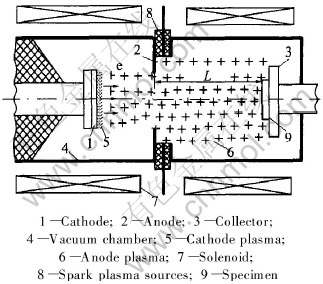
Fig.1 Schematic diagram of HCPEB source
Sliding friction and wear tests were conducted using a ball-on-flat apparatus, which is illustrated schematically in Fig.2. Type WC balls were used as the sliding counterfaces in all tests, A sphere-flat contact configuration was used (Fig.2). The reciprocating movement of given amplitude was fully controlled by computer. Diameter of WC balls 5mm, applied force 5N, velocity profile 1mm/s, test length 6m, and stroke length 5mm.
The tests were performed in air-conditioned room. All the surfaces were cleaned with alcohol before friction and wear test. After the tests, all specimens were ultrasonically cleaned in acetone to remove the loosely bound debris on the wear surface and the wear scar was analyzed by scanning electron microscopy(SEM) and the EDAX. The total wear volume loss can be calculated by surface grinding width.
Table 2 HCPEB treatment of magnesium alloys(AZ31, AZ91HP)
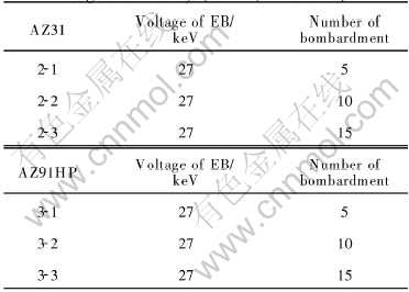
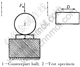
Fig.2 Sliding friction test configuration
3 RESULTS
3.1 Microscopic analysis before and after HCPEB treatment
The typical surface morphologies of some specimens are shown in Fig.3, including the treated and untreated samples. It can be found that sample surface is completely remelted after HCPEB treatment (Figs.3(a), (b)), and the roughness increases. Investigations have shown that, for AZ31, the surface roughness increases fast with the first five shots, then reaches a certain value slowly, from 0.2��m for initial sample to 0.4��m for sample treated with 15 pulses. This roughness is still within the range of industrial requirement. As is well known, crater morphology is the typical surface morphology of the metallic materials treated by pulsed energetic beams. Under the same treating conditions, it was found that, crater density on the surface of AZ91HP is higher than that of AZ31, which is due to the high density of drawbacks in the as cast AZ91HP, on the other hand, the Mg17Al12 particles in AZ91HP also play an important role in the formation of craters[18-20 ].

Fig.3 Surface microstructures of magnesium alloys AZ31 and AZ91HP after HCPEB treatment
Figs.3(c) and (d) show the surface BSE microstructures of AZ91HP before and after HCPEB treatment, it can be found that in the as-received sample there are many large sized and nonhomogeneous intermetallic phase Mg17Al12. After HCPEB bombardment, Mg17Al12 has been resolved and become little round particles or even disappear completely (Figs.3(c) and (d)), this strengthens surface of treated samples and improves sliding wear resistance, which will be discussed in the following in detail. Element distribution in re-melted surface layer becomes more homogeneous and the size of Mg17Al12 becomes smaller. For AZ31, no remarkable difference was observed between as-received and treated samples through BSE image.
3.2 XRD characteristics
Fig.4 shows the XRD pattern of magnesium alloy AZ31 and AZ91HP before and after HCPEB treatment. After HCPEB treatment, the diffraction peaks of magnesium move to higher angles and consequently smaller lattice spacing. This means a large residual compressive stress exists in the surface of the modified samples and causes surface elastic deformation. The intermetallic phase Mg17Al12 in the as-received AZ91HP sample almost disappears after the treatment, making the surface layer a supersaturated solid solution, which is consistent with the BSE result of surface melted layer (Fig.3). This is due to the mixing occurring during the melting process and the solute trapping effect during the fast solidification process. Both residual compressive stress and solid solute of second phase cause the movement of diffraction peaks of magnesium.
3.3 Cross-sectional microhardness distribution
The cross-sectional microhardness distributions of two treated specimens are shown in Fig.5. It can be found that, the microhardness increases and its profile fluctuates in the measured range, and the maximum doesn��t lie in the outmost layer, but in the sub-surface layer. For AZ31, the peak value of microhardness is about 130HK at the depth of 200��m; while for AZ91HP, the peak value is about 120HK at depth of 20��m. Numeric simulation[8] shows that, the characteristic thickness of the melted layer is 4-6��m, and the depth of the heat-affected zone (HAZ) doesn��t exceed 40��m, but measurements show that, the modified layer depth reaches over 250��m, far exceeds the HAZ. Calculation of temperature coupled stress field has shown that, a quasi-static thermal stress formed in the HAZ before melting, which has amplitude of about several hundred MPa, while a shock thermal stress wave with the same amplitude formed during the melting process, and propagates into the deeper layer. Both exceed the yield strength of materials and result in the deformation of the surface layer and so increase microhardness due to normal work hardening effect.

Fig.4 XRD patterns of AZ31(a) and AZ91HP(b) of as-received and treated samples

Fig.5 Sectional microhardness distributions of AZ31 and AZ91HP before and after HCPEB treatment
3.4 Friction and wear behavior
3.4.1 Friction coefficient data
In order to evaluate the effect of HCPEB treatment on wear resistance of magnesium alloys, the friction and wear behaviors of AZ31 and AZ91HP before and after HCPEB treatment were tested under the same condition. Compared with as-received sample, the average friction coefficient reduces slightly after HCPEB treatment. The friction coefficient of the treated sample increases first because of roughness of surface, then reduces and shows fluctuation with increase in grinding crack depth(Fig.6).
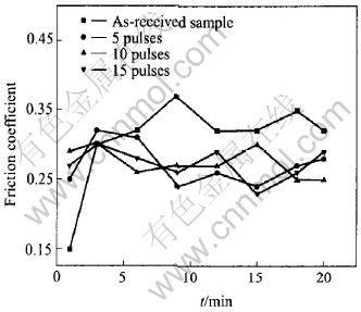
Fig.6 Friction coefficient(��) as function of testing time(t) for Mg-alloys AZ31 before and after HCPEB treatment

Fig.7 Average friction coefficient and wear volume change before and after HCPEB treatment
3.4.2 Wear data
Wear data for AZ31 and AZ91HP in reciprocating test are summarized in Fig.7. Under the same experimental condition, wear rates (WRs) of AZ31 reduce significantly after HCPEB treatment. For AZ91HP, wear resistance of the sample treated for 10 pulses is the best among all treated samples.
4 DISCUSSION
Fig.6 shows the variation of the friction co-efficient with sliding time. At the beginning of the friction test, the friction coefficient of the as-received sample is low (��=0.15), which is caused by dense hard oxide layer on Mg-alloys. After five cycles (sliding 0.05m in distance), the oxide layer is worn out, therefore severe abrasive wear and plastic deformation occurs. So friction coefficient increases sharply. Contrary to as-received sample, the friction coefficient of treated sample is relatively low and stable compared with as-received sample. The friction coefficient is high at the beginning of friction of the friction test. It is because the layer of oxidation on Mg-alloys is destroyed in the process of HCPEB irradiation and can not be recovered again. According to Fig.7(b), for AZ31, it can be seen that wear volume reduces with increase of pulses time. This is due to the fact that modified layer is further extended with increase in pulsed time. The best result is found for 15 pulses treatment, with a relative wear resistance of 6.7. For AZ91HP, although modified layer becomes deep with increasing in pulsed time, relative wear resistance is not improved simply is because hard intermetallic phase Mg17Al12 that reduces at the same time and its strengthening effect disappears.
Evidence based on the examination of the wear tracks suggests that the material removal processes are dominated by localized plastic deformation and the production of long, continuous grooves by plowing. This is typical morphology of abrasive wear, and caused by the fact that the hardness of WC is much higher than those of Mg-alloys AZ31 and AZ91HP. Repetitive plastic grooving is also associated with the fatigue and fracture of inter-groove ridges, as illustrated in Figs.8(a) and (b). The edge fracture process results in the formation of thin shards of wear debris (Fig.8(c)). Most of these elongated particles are crushed before leaving the contact, and thus only a few long, thin shards survived intact to leave the wear interface. The highly localized deformation of grains in the vicinity of sharp grooves at the bottom of the wear tracks is shown in Fig.8(d).
While HCPEB bombardment, the concentrated energy fluxes acting on the Mg alloys induce dynamic temperature fields in the surface layers to which the energy has been deposited, giving rise to superfast heating, melting, and evaporation, followed by superfast solidification in the melt zone of the material. The dynamic stress fields formed cause intense deformation processes in the material, which may impart the material with improved physicochemical and strength properties. These processes in combination make surface layers rich in Al content, which have been confirmed by EDX, solid solution of Mg17Al12 confirmed by BSE of SEM. All these improve the wear resistance of the materials.
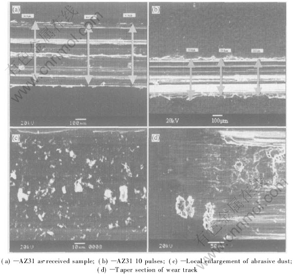
Fig.8 Wear surface characteristics of as-received and treated samples
5 CONCLUSIONS
1) Plastic deformation and dissolution of second phase Mg17Al12 takes place on the surface of material during bombardment by HCPEB. This is mainly caused by the superfast melting of the near-surface layer during HCPEB treatment.
2) HCPEB treatment induces a residual compressive stress on the material surface; the microhardness of surface layer increases significantly.
3) The HCPEB treatment can efficiently improve the friction wear-resistant performance of magnesium alloys AZ31 and AZ91HP in the test range of this paper.
REFERENCES
[1]Mordike B L, Ebert T. Mganesium properties��applications��potential [J]. Materials Science and Engineering A, 2001(302): 37-45.
[2]Eliezer D. Magnesium science, technology and applications [J]. Advanced Performance Mater, 1998(5): 201-212.
[3]Proskurovsky D I, Rotshtein V P, Ozur G E, et al. Physical foundations for surface treatment of materials with low energy, high current electron beams [J]. Surface and Coat Technol, 2000, 125: 49-56..
[4]Korenev S A, Coll B F, Perry A J. Very high rate coating deposition with intense ion and/or electron bombardment [J]. Surface and Coatings Technology, 1996, 86-87: 292-301.
[5]Petrov P, Georgiev C, Petrov G. Experimental investigation of weld pool formation in electron beam welding [J]. Vacuum, 1998, 51: 339-343.
[6]Koleva E. Statistical modeling and computer programs for optimization of the electron beam welding of stainless steel [J]. Vacuum, 2001, 62: 151-157.
[7]Nunes A C, Fragomeni J M Jr. The low pressure gas effects on the potency of an electron beam on ceramic fabric materials for space welding [J]. Acta Astronautica, 2002, 50: 13-25.
[8]Yilbas B S, Sami M, Nickel J, et al. Introduction into the electron beam welding of austenitic 321-type stainless steel [J]. Journal of Materials Processing Technology, 1998, 82: 13-20.
[9]Wykes M, Punshon C, Jones L, et al. All-position reduced pressure electron beam welding for large fusion containment vessels [J]. Fusion Engineering and Design, 2001, 58-59: 793-796.
[10]QIN Ying, DONG Chuang, WANG Xiao-gang, et al. Temperature profile and crater formation induced by high current pulsed electron beam processing [J]. Journal of Vacuum Science Technology, 2003(10): 1934-1938.
[11]Ainley E, Nordquist K, Resnick D J, et al. Process optimization of a chemically amplified negative resist for electron beam exposure and mask making applications [J]. Microelectronic Engineering, 1999, 46: 375-378.
[12]Elsner H, Meyer H G, Voigt A, et al. Evaluation of ma-N 2400 series DUV photoresist for electron beam exposure [J]. Microelectronic Engineering, 1999, 46: 389-392.
[13]Robinson A P G, Palmer R E, Tada T, et al. Exposure mechanism of fullerence derivative electron beam resists [J]. Chemical Physics Letters, 1999, 312: 469-474.
[14]Gueorguiev Y, Vutova K, Mladenov G. Numerical modeling of the processes of exposure and development in electron beam lithography on high-temperature superconductor thin films [J]. Thin Solid Films, 1998, 323: 222-226.
[15]Thoms S, Macintyre D. Process optimization of DUV photoresists for electron beam lithography [J]. Microelectronic Engineering, 1996, 46: 287-290.
[16]Dong C, Wu A, Hao S, et al. Surface treatment by high current pulsed electron beam [J]. Surface and Coatings Technology, 2003, 163-164: 620-624.
[17]WU Ai-min, CHEN Jing-song, ZHANG Ai-min, et al. Study on the die steel surface modification by electron beam [J]. Nuclear Techniques, 2002, 25(8): 608-614. (in Chinese)
[18]ZOU Jian-xin, QIN Ying, DONG Chuang, et al. Numerical simulation of the thermal-mechanical process of high current pulsed electron beam treatment [J]. Journal of Vacuum Science & Technology, 2003, A22(3): 545-552.
[19]ZOU Jian-xin, WU Ai-min, DONG Chuang, HAO Shen-zhi, et al. Oxidation protection of AISI H13 steel by high current pulsed electron beam treatment [J]. Surface and Coatings Technology 2004, 183: 261-267.
[20]Proskurovsky D I, Rotshtein V P, Ozur G E, et al. Pulsed electron-beam technology for surface modification of metallic materials [J]. Journal of Vacuum Science & Technology A: Vacuum, Surfaces, and Films, 1998, 16(4): 2480-2488.
Received date: 2005-01-17; Accepted date:2005-06-29
Correspondence: GAO Bo, PhD; Tel: +86-24-83680527; E-mail: Surfgao@yahoo.com.cn
