
J. Cent. South Univ. (2012) 19: 791-796
DOI: 10.1007/s11771-012-1073-7![]()
Using HF rather than NH4F as doping source for
spray-deposited SnO2:F thin films
S. J. Ikhmayies1, R. N. Ahmad-Bitar2
1. Department of Basic Sciences-Physics, Faculty of Information Technology,Al Isra University, Amman 16197, Jordan;
2. Physics Department, Faculty of Science, University of Jordan, Amman 11942, Jordan
? Central South University Press and Springer-Verlag Berlin Heidelberg 2012
Abstract:
Fluorine doped tin oxide SnO2:F thin films were prepared by the spray pyrolysis (SP) technique on glass substrates by using SnCl2��2H2O as a precursor and NH4F and HF as doping compounds. A comparison between the properties of the films obtained by using the two doping compounds was performed by using I-V characteristics in the dark at room temperature, AC measurements, and transmittance. It is found that the films prepared by using HF have smaller resistivity, lower impedance and they are less capacitive than films prepared by using NH4F. In addition, these films have higher transmittance, higher optical bandgap energy and narrower Urbach tail width. These results are interesting for the use of SnO2:F as forecontact in CdS/CdTe solar cells.
Key words:
CdS/CdTe solar cells; transparent conducting oxides; spray pyrolysis; doping��
1 Introduction
Tin oxide (SnO2) is a wide bandgap nonstoichiometric semiconductor with a low n-type resistivity (��10-3 ����cm) and high transparency (��90%) in the visible region [1]. Optical, electrical and structural properties of this compound make it very attractive for many kinds of applications in opto-electronic devices, gas sensors and solar collectors [2]. In addition, chemical and mechanical stability of SnO2 films makes them suitable for many other applications such as transparent conductive coatings and heterojunction solar cells [3]. Among various dopants for SnO2, fluorine is often preferred, because fluorine doping results in films with high transparency and good conductivity [3]. Different sources of fluorine were used to produce SnO2:F thin films, such as ammonium fluoride (NH4F) and hydrofluoric acid (HF). A lot of researchers used NH4F [4-8] and others used HF [1, 3, 7-8] for doping SnO2 films. GORDILLO et al [8] used both of NH4F and HF and showed that the resistivity of thin films obtained by using HF was lower than that of similar films obtained by using NH4F by a factor of 2.2. They also found that the films obtained by using HF have more random orientations.
Fabrication techniques used to prepare tin oxide include dip coating [2], evaporation [9], reactive sputtering [10], chemical vapor deposition [9, 11], and spray pyrolysis [1, 12-15]. The latter method enables the production of films of large area, high quality and low cost and doping can be achieved by adding a suitable compound of the dopant to the spray solution.
ELANGOVAN and RAMAMURTHI [16] used SnCl2 and NH4F and produced SnO2:F thin films by the spray pyrolysis technique, and they studied the optoelectronic properties of the films to be used as window materials in solar cells. RIVEROS et al [17] used SnCl2 and HF to prepare SnO2:F thin films by the same technique and studied their optical and structural properties. According to our knowledge, just GORDILLO et al [8] used both of NH4F and HF and made a comparison between the produced films and this study was performed in 1994. In this work, we prepared SnO2:F by the same technique and used SnCl2 and both of HF and NH4F as doping compounds.
2 Experimental
Stannous chloride SnCl2��2H2O was used in making the precursor solution for SnO2 thin films. Ammonium fluoride NH4F (BDH Chemicals Ltd. Poole, England) and hydrofluoric acid HF (40%) were tried as the doping materials. Two different solutions were prepared: The first solution was made from 5.03��10-3 mol of SnCl2��2H2O and 4.73��10-3 mol of NH4F dissolved in 45 mL of methanol CH3OH (May and Baker Ltd. Dagenham, England), 5 mL of distilled water and 1 mL of HCl. The ratio of fluorine ions to tin ions in this solution was 0.94 approximately the same as that of GORDILLO et al [8] at which they got the smallest resistivity and highest transmittance. The set of films prepared from this solution is called NH4F-films. The second solution was made by dissolving 5.01��10-3 mol of SnCl2��2H2O with 5.71��10-3 mol of HF in 45 mL of methanol, 5 mL of distilled water and 1 mL of HCl. The ratio of fluorine ions to tin ions in the solution was 1.14, also the same as GORDILLO et al [8] at which they got the smallest resistivity and highest transmittance. The set of films prepared from this solution is called HF-films.
The substrates were ordinary glass slides with dimensions of 2.5 cm��6 cm��0.1 cm. They were first cleaned by dipping in distilled water to remove the dust, and then in methanol for ultrasonic cleaning for at least 15 min. Finally, they were soaked in distilled water and polished with lens paper. The pre-treatment of the substrates was carried out to facilitate nucleation on the substrate surface. Presence of contamination on the substrate surface is one of the reasons of the appearance of pinholes.
The experimental set-up used for film deposition has been described elsewhere [12]. The spray rate was usually in the range of 2-5 mL/min. The optimum carrier gas pressure for this rate of solution flow was around 5 kg/cm2, where nitrogen was used as the carrier gas. At lower pressures, the size of the solution droplets becomes large, which results in the presence of recognized spots on the films and then less transparency. This situation increases the scattering of light from the surface and then reduces the transmittance of the films.
The I-V measurements were taken at room temperature by a system that consists of a Keithley 6512 programmable electrometer capable of measuring a current of 10-15 A, and Digistant type 6405 power supply. The sample was placed in a brass cell which enables us to take the measurements in the dark. Silver was used as the contact material for SnO2:F thin films. Two strips of silver were deposited on the surface of the film by vacuum evaporation. The strips are of thickness around 0.4 ��m, length of 1 cm, width of 1 mm, and separation of 2-3 mm. AC measurements were performed with HP LCR meter 4284A spanning the frequency range from 20 Hz to 1 MHz.
The transmittance of the films was measured in the wavelength range (��) of 290-1 100 nm by using a double beam Shimadzu UV 1601 (PC) spectrophotometer with respect to a piece of glass of the same kind of the substrates. For films of transmittance containing minima and maxima, the following relation was used to estimate the thickness [18].
Consider the transmittance at a certain maximum as Tmax, the transmittance at the next minimum as Tmin and dispersion is negligible, then define a parameter ��T by the approximate form:
![]() (1)
(1)
where n0, n1, and n2 are the refractive indices of air, film, and glass, respectively, and the conditions ![]() and n2<>1 are satisfied. Solving Eq. (1) for n1 to have
and n2<>1 are satisfied. Solving Eq. (1) for n1 to have
 (2)
(2)
And the film thickness is given by
![]() (3)
(3)
where ��min and ��max are the values of the wavelength at a certain maximum and the next minimum, respectively.
For films with transmittance that does not show such maxima and minima, Lambert law for absorption in a semiconductor was used to estimate the thickness. Thickness estimated by the last method and transmittance at a certain wavelength (i.e. ��=310 nm) which lies below the cut-off wavelength were substituted in Lambert law to deduce the absorption coefficient (��). The thickness of the films was estimated by using this value of �� and transmittance of each film at the afore-mentioned wavelength.
3 Results and discussion
3.1 DC and AC measurements
DC and AC measurements were used to investigate the electrical properties of the films. DC measurements were represented by the I-V plots in the dark at room temperature. AC measurements were represented by measuring impedance, capacitive reactance and phase angle, where the results are the same in the dark and light.
Figure 1 depicts the I-V characteristics of two SnO2:F thin films with thickness of about 100 nm. One of the NH4F-films and the other of the HF-films are deposited at a substrate temperature Ts=450 ��C. From Fig. 1, the resistivity of the HF-film is 2.71 ����cm, while that of the NH4F-film is 183 ����cm, which means that the resistivity is decreased by a factor of about 67.5 by using HF as the doping compound. GORDILLO et al [8] got a reduction by a factor of 2.2 but they got smaller values of resistivity. The difference between the behaviour of resistivity with temperature in our work and their work is that they got a minimum of resistivity located at Ts��400 ��C for the HF-films and at Ts��350 ��C for the NH4-films. According to our previous work [14], the resistivity was found to decrease with the substrate temperature.
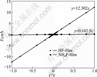
Fig. 1 I-V characteristics of two SnO2:F thin films with thickness of about 100 nm
The large difference in the reduction factor of the resistivity may be that they did not mention any addition of HCl to their solutions, but we added HCl to both solutions. The improvement in the electrical properties of the HF-films may be due to the higher concentrations of fluorine and chlorine in these films. It is the thermal decomposition products of NH4F escaping into the atmosphere that results in smaller concentrations of fluorine [4, 6] and chlorine in the films doped by using this compound. The following reactions are most probable [19]:
NH4F?NH3 + HF (4)
NH3+HCl?NH4Cl (5)
where NH4Cl decomposes at elevated temperatures [19].
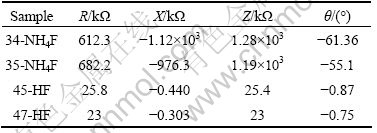
Table 1 gives the AC measurements taken at room temperature for two films of each set. The measurements are found to be the same in the dark and in the light. It is noticed that the resistance (R), capacitive reactance (X) and impedance (Z) of the NH4F-films are larger than those of the HF-films. The phase angle (��) is negligible for the HF-films but it is large for the NH4F-films. This means that the HF-films are approximately non-capacitive, while the NH4F-films are capacitive. This capacitive behaviour is most probably attributed to a potential between grains on the grain boundaries, and it is a main reason of the high resistivity of these films.
Table 1 AC measurements for NH4F-films and HF-films with thickness of about 100 nm taken at frequency of 1 kHz
3.3 Optical properties
Transmittance curves were measured in the wavelength range of 290-1100 nm at room temperature for the two sets of films and they are displayed in Fig. 2. It is noticed that, first, the transmittance of the HF-films is larger than that of the NH4F-films despite the fact that they have larger thickness. Second, the knee at the absorption edge which is an indication of the high quality of thin films is more apparent on the transmittance curves of the HF-films, but it is not seen in the case of the NH4F-films. Third, tailing towards longer wavelengths is more evident on the transmittance curves of the NH4F-films. All of these observations confirm that the quality of the HF-films is better, so they are more appropriate for the use as forecontacts in the CdS/CdTe solar cells.
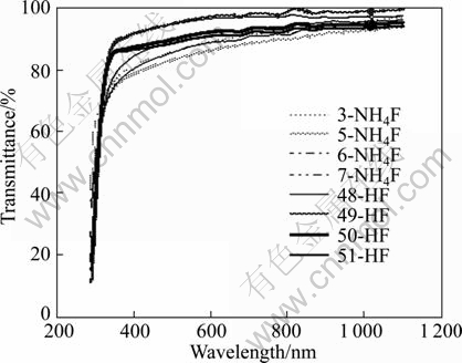
Fig. 2 Transmittance curves of SnO2:F thin films doped by using NH4F and HF deposited at substrate temperature of 450 ��C (Thickness of NH4F-films is 230-340 nm and that of HF-films is 320-390 nm)
GORDILLO et al [8] studied the relation between transmittance and F- concentration in the solution for SnO2:F thin films with HF and NH4F as dopant compounds and SnCl2 and SnCl4 as precursors. They found that the introduction of F- impurity to the SnO2 films does not affect significantly the transmittance of the samples, especially at wavelengths greater than 600 nm. But, there is a slight increase of the transmittance with F- concentration in the solution. So, our results are in good agreement with their results.
To investigate the optical bandgap energy Eg, the absorbance was deduced from the transmittance curves and its first derivative was used for this purpose. The minima in the first derivative refer to the values of Eg. Figure 3 depicts the curves of the first derivative against wavelength for the two sets of films. Figure 3(a) shows these plots for the NH4F-films, while Fig. 3(b) shows the plots for the HF-films. A comparison between the two figures shows that minima in Fig. 3(a) have structure, while no structure appears in Fig. 3(b). This means that resolving the peaks by a deconvolution peak fit can be used, and different peaks mean different values of the bandgap energy. The presence of more than one bandgap may indicate the presence of other phases of SnO2 in the films and/or the presence of different sizes of the grains, since the bandgap increases when the grain size decreases, especially if the grain size is in nanometres. In Fig. 3(b), the minima are deeper and they have no structure, which means that a single bandgap is presented and no apparent effect of grain size is found. Then, we conclude that larger grains are formed in the HF-films with narrower grain size distribution.
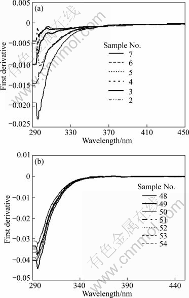
Fig. 3 First derivative curves of SnO2:F thin films: (a) For NH4F-films; (b) For HF-films (Numbers in legends refer to sample��s numbers)
The estimated values of the optical bandgap energy are listed in Table 2. It is apparent that the bandgap energy of the HF-films is larger than that of the NH4F-films, which is better for the use as a forecontact in the CdS/CdTe solar cells. The larger values of bandgap energy in the HF-films can be attributed to a higher fluorine and/or chlorine concentration in these films and so it is due to the Moss-Burstein effect [1, 4].
The absorption coefficient �� was deduced from the transmittance curves and displayed in Fig. 4 as a function of the photon��s energy h�� , where h is Planck��s constant and �� is the frequency of the radiation. A comparison between the curves in Fig. 4(a) and Fig. 4(b) shows that the HF-films have lower absorption coefficient for energies less than the bandgap energy, but they show a stronger increase of the absorption coefficient with photon��s energy for energies larger than the bandgap. So, the HF-films can pass more light to the window layer in CdS/CdTe solar cells than the NH4F films. The curves in Fig. 4(a) are similar to those obtained for spray-deposited SnO2 films obtained by MELSHEIMER and ZIEGLER [20] where the substrate temperature is in the range of 420-460 ��C and the films are composed of polycrystallines. On the other hand, the curves in Fig. 4(b) are similar to the curves obtained by the same authors [20] for partially polycrystalline films.
Table 2 Bandgap energies and values of Urbach tail width of two sets of films with corresponding values of film thickness
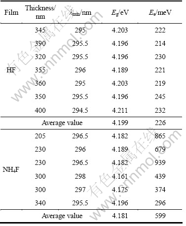
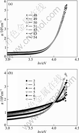
Fig. 4 Plots of absorption coefficient �� against photon��s energy h��: (a) For HF-films; (b) For NH4F-films
In the low photon energy range, it is assumed that the spectral dependence of the absorption edge follows the empirical Urbach rule given by [21]
��=��0exp(hn/Ee) (6)
where ��0 is a constant and Ee is the width of the Urbach tail. The exponential tail appears because disordered and amorphous materials produce localized states extended in the bandgap. A plot of ln�� against the photon��s energy is shown in Fig. 5. To obtain the width of Urbach tail, a linear fit was established in the linear portions of the curves and the results are listed in Table 2. Comparing these values for the two sets of SnO2:F films, it is found that the values of Ee for HF-films are much smaller than those for NH4F-films. MELSHEIMER and ZIEGLER [20] got the width of Urbach tail for undoped SnO2 films by the spray pyrolysis technique. For the substrate temperature range of 420-500 ��C, they got Ee=210-250 meV where the films are polycrystalline type. Our values for HF-films for Ts=450 ��C are in the range of 214-245 meV which are approximately the same as the values obtained by them. Our values of Ee for NH4F-films which are in the range of 296-939 meV are sometimes close and sometimes larger than the values by these authors [20] obtained for amorphous and partially polycrystalline SnO2 films where they got Ee=350-550 meV.
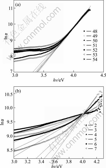
Fig. 5 Plots and linear fit of ln�� against photon��s energy: (a) For HF-films; (b) For NH4F-films
In another work [15], we got the values of the Urbach tail for vacuum evaporated SnO2 thin films Ee=471-646 meV where the films are found to be partially polycrystalline. According to MELSHEIMER and ZIEGLER [20], the widths of Urbach tails increase with increasing structural disorder and are almost constant for each state of order (amorphous, partially polycrystalline and polycrystalline).
4 Conclusions
1) SnO2:F thin films prepared by the SP technique on glass substrates were produced by using SnCl2��2H2O in making the precursor solution and HF and NH4F as the doping compounds.
2) It is found that films produced by using HF as a source of fluorine have better quality than those prepared by using NH4F. From the I-V plots, it is found that these films have smaller resistivity. From the AC measurements, it is shown that these films are less capacitive. The investigation of transmittance spectra shows that these films have higher transmittance, larger bandgap energy and narrower width of Urbach tail.
3) All of these findings are of great interest for the use of SnO2:F as a forecontact in the CdS/CdTe solar cells.
Acknowledgment
The authors thank S. Farrash from the Physics Department of the University of Jordan for making the contacts by vacuum evaporation.
References
[1] Rakhshani A E, Makdisi Y, Ramazaniyan H A. Electronic and optical properties of fluorine-doped tin oxide films [J]. J Appl Phys, 1998, 83(2): 1049-1057.
[2] Geraldo V, de ANDRADE S L V, de Morais E A, Santilli C V, Pulcinelli S H [J]. Sb doping effect and oxygen adsorption in SnO2 thin films deposited via sol-gel [J]. Mat Res, 2003, 6(4): 451-456.
[3] Banerjee A. Maity N R. Kundoo S, Chattopadhyay K. K. Poole�CFrenkel effect in nanocrystalline SnO2:F thin films prepared by a sol�Cgel dip-coating technique [J]. Phys Stat Sol A, 2004, 201(5): 983-989.
[4] Shanthi E, Banerjee A, Dutta V, Chopra L K. Electrical and optical properties of tin oxide films doped with F and (Sb + F) [J]. J Appl Phys, 1982, 53(3): 1615-1621.
[5] Yadav A A, Masumdar E U, Moholkar A V, Neumann- Spallart M, Rajpure K Y, Bhosale C H. Electrical, structural and optical properties of SnO2:F thin films: Effect of the substrate temperature [J]. Journal of Alloys and Compounds, 2009, 488: 350-355.
[6] Bruneaux J, Cachet H, Froment M, Messad A. Correlation between structural and electrical properties of sprayed tin oxide films with and without fluorine doping [J]. Thin Solid Films, 1991, 197: 129-142.
[7] Abdul Gafor W S A, Mohammed M T. The role of the chemical doping on the optical and electrical properties of tin oxide films [J]. Iraqi J of Chem, 1992, 17(1): 188-191.
[8] Gordillo G, Moreno L C, de la Cruz W, Teheran P. Preparation and characterization of SnO2 thin films deposited by spray pyrolysis from SnCl2 and SnCl4 precursors [J]. Thin Solid Films, 1994, 252: 61-66.
[9] Montmeat P. Thin film membranes for the improvement of gas sensor selectivity [D]. ?cole Nationale Sup��rieure des Mines de Saint-?tienne (ENSMSE): Graduate School for Science and Technology, France, 1999.
[10] Pan S S, Ye C, Teng X M, Fan H T, Li G H. Preparation and characterization of nitrogen-incorporated SnO2 Films [J]. Appl Phys A, 2006, 85(1): 21-24.
[11] Sundqvist J, H?rsta A. Growth of SnO2 thin films by ALD and CVD: A comparative study [C]// Proceedings of the Sixteenth Int. CVD Conf. Paris, France, 2003: 511.
[12] Ikhmayies S J. Production and characterization of CdS/CdTe thin film photovoltaic solar cells of potential industrial use [D]. Amman: University of Jordan. 2002.
[13] Elangovan E, Ramamurthi K. Studies on optical properties of polycrystalline SnO2:Sb thin films prepared using SnCl2 precursor [J]. Cryst Res Technol, 2003, 38(9): 779-784.
[14] Ikhmayies S J, Ahmad-Bitar R N. Effect of the substrate temperature on the electrical and structural properties of spray-deposited SnO2:F thin films [J]. Materials Science in Semiconductor Processing, 2009, 12: 122-125.
[15] Ikhmayies S J, Ahmad-Bitar R N. An investigation of the bandgap and Urbach tail of vacuum-evaporated SnO2 thin films [C]// Proceedings of the Eleventh World Renewable Energy Congress and Exhibition. Abu Dhabi, United Arab Emirates, 2010: 967-972.
[16] Elangovan E, Ramamurthi K. Optoelectronic properties of spray deposited SnO2:F thin films for window materials in solar cells [J]. Journal of Optoelectronics and Advanced Materials, 2003, 5(1): 45-54.
[17] Riveros R, Romero E, Gordillo G. Synthesis and characterization of highly transparent and conductive SnO2:F and In2O3:Sn thin films deposited by spray pyrolysis [J]. Brazilian Journal of Physics, 2006, 36(3B): 1042-1045.
[18] Alvin G M. Optical interference method for the approximate determination of refractive index and thickness of a transparent layer [J]. Applied Optics, 1978, 17(17): 2779-2787.
[19] Bloss W H, Schock W H. CdS-CuxS thin film solar cells. In: Photovoltaic and photoelectrochemical solar energy conversion [M]. New York and London: Nato Advanced Study Institute Series, Plenum Press, 1980: 117-156.
[20] Melsheimer J, Ziegler D. Band gap energy and Urbach tail studies of amorphous, partially crystalline and polycrystalline tin dioxide [J]. Thin Solid Films, 1985, 129: 35-47.
[21] Natsume Y, Sakata H, Hirayama T. Low temperature electrical conductivity and optical absorption edge of ZnO films prepared by chemical vapor deposition [J]. Phys Stat Sol A, 1995, 148: 485-495.
(Edited by YANG Bing)
Received date: 2011-07-26; Accepted date: 2011-11-14
Corresponding author: S. J. Ikhmayies, PhD; Tel: +962-79-5893884; E-mail: shadia_ikhmayies@yahoo.com
Abstract: Fluorine doped tin oxide SnO2:F thin films were prepared by the spray pyrolysis (SP) technique on glass substrates by using SnCl2��2H2O as a precursor and NH4F and HF as doping compounds. A comparison between the properties of the films obtained by using the two doping compounds was performed by using I-V characteristics in the dark at room temperature, AC measurements, and transmittance. It is found that the films prepared by using HF have smaller resistivity, lower impedance and they are less capacitive than films prepared by using NH4F. In addition, these films have higher transmittance, higher optical bandgap energy and narrower Urbach tail width. These results are interesting for the use of SnO2:F as forecontact in CdS/CdTe solar cells.
