
Photocatalytic degradation characteristic of amorphous TiO2-W thin films deposited by magnetron sputtering
HUANG Jia-mu(�Ƽ�ľ), LI Yue-xia(����ϼ), ZHAO Guo-dong(�Թ���), CAI Xiao-ping(��Сƽ)
College of Materials Science and Engineering, Chongqing University, Chongqing 400045, China
Received 10 April 2006; accepted 25 April 2006
Abstract:
TiO2-W films were deposited on the slides by reactive magnetron sputtering. Properties of the films were analyzed via AFM, XRD, XPS, STS, UV-Vis and ellipse polarization apparatus. The results show that TiO2-W films are amorphous. The AFM map reveals that the surface of the film is tough and porous. The experiments of decomposing methylene blue indicate that the thickness threshold on these films is 141 nm, at which the rate of photodegradation is 90% in 2 h. And when the thickness is over 141 nm, the rate of photodegradation does not increase any more. This result is completely different from that of crystalloid TiO2 thin film.
Key words:
amorphous TiO2; TiO2-W thin films; magnetron sputtering; photocatalysis; threshold;
1 Introduction
The decomposition of TiO2 photocatalytic degradation is a newly developed technology with a great potential for further exploitation and application. Researches have revealed that TiO2 activation only occurs under the neo-ultraviolet whose wavelength is shorter than 387.5 nm (approximately 3.2 eV), resulting in a low utilization of solar light and photons rate. Metal-ion-doped TiO2 can improve the photocatalytic degradation or widen the light response spectrum of TiO2. Up till now, many researches on the metal-ion-doped TiO2 mainly focus on the crystalloid TiO2 and little attention has been paid to the amorphous TiO2 due to its lack of photocatalytic activity.
As amorphous ZnS and CdS are ready candidates for photocatalyzers while amorphous and crystal semiconductors have similar band structure, this paper will study on the W-doped amorphous TiO2 to improve its photocatalytic activation.
Though there are a number of methods for TiO2 film preparation, sol-gel method is the one that is the most widely used. This film coating technique is relatively mature, but the mechanical durability is not enough for practical uses. In addition, the uniformity of the thickness in a large area is poor.
Compared with the sol-gel method, magnetron sputtering method has strongpoint of the high quality films with high density, high adhesion, and high hardness. The film prepared at low temperature, in particular, has a good uniformity of the film thickness in a large area. Therefore, the TiO2-W films were deposited on the slides by reactive magnetron sputtering in this experiment and the photocatalytic degradation characteristics and other pertinent features of the films were studied.
2 Experimental2.1 Preparation of amorphous TiO2-W films
Amorphous TiO2-W films were deposited by the co-sputtering of reactive direct current(DC) and radio-frequency(RF) magnetron sputtering with a thickness of less than 200 nm. The distance between the butt and the substrate was 10 cm, the base pressure before sputtering in the coating chamber was less than 5��10-3 Pa. At the same time the sputtering power and sputtering time of the RF port were controlled to dope tungsten. The DC sputtering power was 350 W, the working pressure of the coating chamber was 1.0 Pa, the substrate temperature was at room temperature��O2 flux was 35 mL/s.
2.2 Evaluation of amorphous TiO2-W film
The XRD analysis of the films was performed on a D/Max-3C diffractometer. The surface morphology of the film was examined on the IPC-205B atom microscope. M2000-U multi-wavelength ellipse polarization apparatus was used to measure the ellipse polarization spectra of TiO2-W films to get the thickness of the films. The photocatalytic activity of the film was evaluated by decomposing methylene blue whose concentration serves as the function of irradiation time. Samples (the size was 25 mm��60 mm for each one), which were coated with different thickness of TiO2-W films, were put at the bottom of the quadrate container(25 mm��60 mm) flatly, and infused the methylene blue liquor into each one. Set the UV light at the height of 300 mm above the sample surface and the sample was irradiated for 2 h. After that, the absorbance change of the liquor, which had been decomposed by TiO2-W film, was checked with the ultraviolet-visible spectrophotometer to ascertain the decoloured rate of the liquor. The relation between the decoloured rate of the methylene blue and the irradiating time of the sample was revealed by the experiment of sample T4��s photocatalytic degradation with different irradiation time of 30, 60, 90, 120 and 150 min, respectively.
3 Results and discussion3.1 Characteristics of TiO2-W thin films
The X-ray diffraction pattern of the sputtered film prepared at room temperature is shown in Fig.1, from which it is clear that all the peaks are amorphous dispersion peaks. It means that the film is amorphous. As doped-W on the TiO2 surface obstructs the growth of the TiO2 crystal nucleus in the substrate, the tungsten atoms have again become the nucleating centres and the existence of several nucleating centers holds back the TiO2 nucleating, crystallization and growth. That is why the film is amorphous. Besides, at the room temperature, it is also not favorable to the crystallization and growth of the TiO2 crystal on the surface of the amorphous
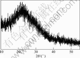
Fig.1 XRD pattern of TiO2-W thin film
substrate glass.
Fig.2(a) shows the picture of TiO2-W film under the atomic force microscope, whose scanning range is 350 nm��350 nm. The picture reveals that the film surface is smooth, the grain size distribution (15-20 nm) is equal with no extraordinarily large granules[7].
Fig.2(b), whose scanning range is 4.6 nm��4.6 nm��manifests that the space between atoms is relatively large, the atom arrangement is in disorder with many equally-distributed pores. The incompact pattern between atoms expands the film surface and the equally-distributed pores can easily capture electrons, making photo-electron-hole transference onto the surface, which effectively improves the photocatalytic degradation of the film[8].
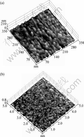
Fig.2 Surface images(AFM) of 140 nm thickness TiO2-W thin film: (a) Scanning area of 350 nm��350 nm; (b) Scanning area of 4.6 nm��4.6 nm
The full-spectrum scanning on the surface components of sample T4 is shown in Fig.3, where the major components of the film are four elements, namely, C, Ti, W and O, among which C is caused by the surface pollution due to its exposure to air and the contamination of a minimum of organic substance in the coating chamber. The narrow-spectrum scanning of the titanium peak and the tungsten peak shows that Ti exists in the form of Ti4+ and W atom in the film adopts two forms, namely, simple substance W and W6+.
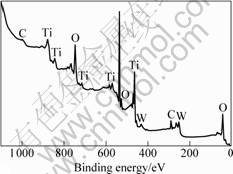
Fig.3 XPS spectrum of sample T4
3.2 Influence of doped-tungsten on optical band of amorphous TiO2
In order to examine the influence of doped-tungsten on catalytic result, experiment was conducted on ultraviolet and visible spectra of amorphous TiO2 film with different degrees of doped-tungsten. The parameters of sample preparation are listed in Table 1 and the spectra obtained by ultraviolet and visible spectrophotometer are shown in Fig.4.
Table 1 Parameters of sample preparation
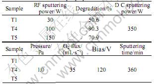
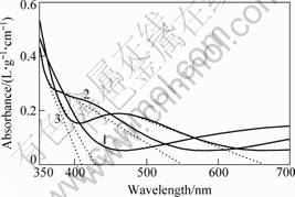
Fig.4 UV-Vis absorption spectra of TiO2-W films
Samples T1, T4 and T5 correspond to curves 1, 2 and 3, respectively. In UV-Vis absorption spectra, the point of intersection between tangent extrapolation and long-wave direction will determine the starting point of the absorption band in the absorption zone. This numerical value corresponds to the absorption edge of the material.
The absorption edge of curve 1 is located at 450 nm with a long weak absorption ending. The absorption edge of curve 2 is situated at 410 nm. A new absorption peak occurs at 375-385 nm, whose absorption edge is at 545nm. The absorption edge of curve 3 is at 425 nm and produces a new peak at 450-470 nm, whose absorption edge is at about 660 nm. A comparison of curves 1, 2 and 3 shows that the corresponding curves of absorption peaks in the high absorption zone in curves 2 and 3 have undergone red shift.
Curve 1 indicates that under 30 W doping power, doped-tungsten leads to the change of band width of TiO2. Based on the formula ��g=1 240/Eg[9], the band width decreases at 2.75 eV.
Both curves 2 and 3 witness new absorption peaks in long wave band. The band gaps of the absorption peak in curve 2 are 3.02 eV and 2.28 eV while those of curve 3 are 2.92 eV and 1.88 eV, which means the existence of impurity level. Therefore, the appropriate doped tungsten will create new energy level in the band-gap of TiO2.
3.3 Photocatalytic activity of amorphous TiO2 film
3.3.1 Influence of doped-tungsten on photocatalytic degradation of amorphous TiO2 film
Fig.5 shows the absorption curve of sample T4��s methylene blue under different irradiation time. Curve a is the absorption curve of methyl blue before irradiation, b, c, d, e and f are the curves after irradiation time of 30, 60, 90, 120 and 150 min, respectively. Fig.6 shows the translation from absorbency to the rate of decomposition. It is obvious that the photocatalytic degradation of TiO2-W film in 120 min reaches 90%.
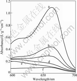
Fig.5 Decomposition of sample T4 in methylene blue solution under UV irradiation
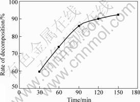
Fig.6 Relationship between irradiating time of sample T4 and rate of decomposition in methylene blue solution
A ure amorphous TiO2 film does not have any catalytic activity. Metal ion doped with crystal TiO2 can enhance the absorption capability of the visible light. The underlying reason is that the adulteration of metal ion into TiO2 crystal lattice results in the occurrence of various regional energy levels in the crystalloid band and meliorate the absorption capability of the visible light[10]. Doping metal ions into amorphous TiO2 can also meliorate the scope of photo response. Though the molecules in amorphous semiconductor are out of order, the semiconductor still contains the microstructure of single crystal, that is, order in short distance. In other words, whatever the form is, crystal or amorphous, the basic combination modes of atoms are the same, only that the bond length and bond angles in the amorphous form undergo certain degree of aberration. So the basic band structures of semiconductors are similar in amorphous and crystal states. Just as the adulteration of metal ion with crystal TiO2 can improve the photocatalytic degradation activity��the doping of metal ion with amorphous TiO2 can also enhance the absorption capability of the catalyst by its introduction of regional energy levels in the band-gap. It is in line with the conclusion reached in the afore-mentioned experiments in which the doped-tungsten in amorphous TiO2 has produced impurity levels.
In XPS analysis, tungsten exists in the forms of simple substance and W6+ in TiO2-W amorphous film. On the one hand, as W6+ is variable ion in d-orbit, its capture of the electrons in the conduction band reduces the compounding of the photoelectron and hole on the TiO2 surface. On the other hand, as W6+ exerts weak bondage upon electrons and its weak ionization energy leads to the transition once it is excited by low-energy photons, exciting by low-energy photons can lead to the occurrence of the transition. The tungsten in simple substance in TiO2 film means a short-circuit micro-cell with TiO2 and pure tungsten as its electrodes. The hole produced by TiO2 pole oxidizes the organic substance in the liquid while the flow of electrons to the metal pole deoxidizes the components in the liquid. Thus the conclusion can be drawn that the appropriate doped-tungsten will enhance photpcatalytic degradation in amorphous TiO2.
3.3.2 Influence of doping quantity on photocatalytic degradation activity in amorphous TiO2
![]() Table 1 shows the photocatalytic degradation of TiO2-W amorphous films with different degree of doping-tungsten. It shows that the excessive tungsten adulteration will reduce the effect of photocatalytic degradation. That is because the excess of WO3 turns the shift centre for free electrons into electrons compounding centre, leading to the fall of the separation rate of photoelectrons and hole. Besides, an excessive existence of WO3 will lead to the form of WO3 glomeration on TiO2 surface��covering the catalytic centre on the surface and depressing the photpcatalytic degradation activity.
Table 1 shows the photocatalytic degradation of TiO2-W amorphous films with different degree of doping-tungsten. It shows that the excessive tungsten adulteration will reduce the effect of photocatalytic degradation. That is because the excess of WO3 turns the shift centre for free electrons into electrons compounding centre, leading to the fall of the separation rate of photoelectrons and hole. Besides, an excessive existence of WO3 will lead to the form of WO3 glomeration on TiO2 surface��covering the catalytic centre on the surface and depressing the photpcatalytic degradation activity.
3.3.3 Influence of film thickness on photocatalytic degradation activity in amorphous TiO2-W
Table 2 lists the TiO2-W film samples with different thickness. The samples undergone 2 h irradiation and the absorbency of methylene blue, as shown in Fig.7, are recorded by ultraviolet-visible spectrophotometer. Curve a is the absorbency of methylene blue before photocatalytic decomposition and curves b, c, d, e, f and g are the respective absorbency of T1-T6 samples after 2 h UV irradiation, among which curves e, f and g superpose each other. By conversing absorbency into decomposition rate, the curve reflecting the relationship between film thickness and photocatalytic decomposition rate is shown in Fig.8.
Table 2 Thickness of samples
![]()
It is clear from Fig.8 that when the film thickness is less than 141 nm, the photocatalytic decomposition rate rises with the increase of thickness of the film. When the thickness equals 141 nm, the photocatalytic decomposi-
tion rate of methylene blue reaches the highest 90%. When the thickness exceeds 141 nm, the photocatalytic decomposition rate becomes stable.
Though photocatalytic degradation is merely surface reaction, the film thickness has great impact upon photocatalytic degradation characteristics. The reason is that the film growth and surface defect vary with the difference in film thickness. The transmission distance of photo-electron-hole and UV diffusion in the film also change with different film thickness. SHENG et al[11] assert that film thickness exercises substantial impact upon photocatalytic degradation and the thicker the film is, the more active the photocatalytic degradation becomes.
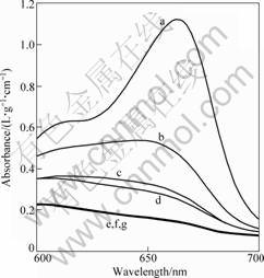
Fig.7 Decomposition of TiO2-W films in methylene blue solution under UV irradiation
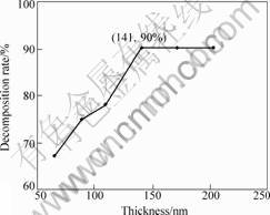
Fig.8 Relationship between thickness of TiO2-W films and decomposition rate in methylene blue solution
According to Fig.8, the photocatalytic degradation rate of amorphous TiO2-W films is enhanced with the increase of film thickness. That is because under UV irradiation, TiO2-W film will produce electron-hole pairs, which spread to the low-consistency area (surface). During the diffusion process the components will compound. As all carriers in theory are able to move to the surface, when the film thickness is less than the diffusion length of the carrier, the increase of film thickness will lead to the augmentation of the carriers that move to the surface. In addition, according to A=1-e-��t[11], the increase of film thickness (t) means the drop of transmission rate (��) and the rise of absorbency (A). In other words, the increase of light photo-electron-
hole indicates the elevation of photocatalytic degradation rate.
Regarding crystal TiO2, SHENG et al[11] believe that after the film thickness comes to certain threshold(150-200 nm) the effectiveness of photo- catalytic degradation demonstrates the strengthening tendency. Contrary to the above results is that in the case of amorphous TiO2-W film prepared in the present experiment, photocatalytic degradation rate does not rise with the thickening of the film when the thickness exceeds 141 nm. Because in the amorphous structure, amorphism leads to the bottleneck in the carrier transmission. As a result, carriers inside cannot spread onto the surface and compounding takes place inside.
4 Conclusions
1) TiO2-W amorphous film is prepared by DC and RF magnetron sputtering method, the film is of equally distributed pores and its grain size ranges from 15 to 20 nm.
2) XPS analysis reveals that Ti in the film exists in the form of Ti4+, there exist two forms of tungsten, namely simple substance W and W6+.
3) The optical band-gap changes with the differentiation of doped-tungsten. The increase of tungsten adulteration leads to new energy levels in TiO2 band-gap.
4) Through the experiments of decomposing methylene blue with films of different thickness, the threshold of TiO2-W amorphous film thickness gained in this experiment is 141 nm. Within this scope, the photocatalytic degradation characteristic is strengthened with the increase of film thickness, while out of this scope, the characteristics become stable.
References
[1] SHUI Miao, YUE Lin-hai, XU Zhu-de. Effect of lanthanum doping on the photocatalytic activity of titanium dioxide[J]. Acta Phys Chim Sinica, 2000, 16(5): 459-463. (in Chinese)
[2] LI Jun-hua, FU Hui-jing, FU Li-xin, HAO Ji-ming. Preparation of metallic ion-doped TiO2 thin films and their photocatalytic performance for toluene degradation[J]. Chin J Catal, 2006, 26(6): 503-507.(in Chinese)
[3] SUN Li-jun, HE Xiang-yang, ZHANG Xue-ping, ZHANG Wen-bin, et al. Investigation of photo- catalytic degradation of m ethytorange insunlight with doped TiO2 film[J]. Chinese Rare Earths, 2005, 26(2): 59-61. (in Chinese)
[4] FAN Cai-mei, XUE Peng, DING Guang-yue, SUN Yan-ping, et al. The preparation of nanoparticle Y3+-doped TiO2 and its photocatalytic activity[J]. Rare Metal Materials and Engineering, 2005, 34(7): 1094-1097. (in Chinese)
[5] DIPAOLA A, GARCIA-LOPEZ E, LKEDA S, OHTANI B, et al. Photocatalytic degradation of organic compounds in aqueous systems by transition metal doped polycrystalline TiO2[J]. Catalysis Today, 2002, 75(1-4): 87-93.
[6] PERAL J, CASADO J, DOMENECH X, et al. Competitive processes in photocatalysis: phenol-sulphide and phenol-cyanide competitive photooxidation over ZnO[J]. Electrochimica Acta, 1989, 34(9): 1335-1338.
[7] L? Wei-gang, YANG De-quan, GUO Yun. Evolution and quantiative correction of distortions in atomicforce microscope images[J]. Phys, 2004, 29(4): 237-240.
[8] GAO Lian, ZHENG Shan, ZHANG Qing-hong, et al. Nanometer TiO2 Photocatalysis Material and Application[M]. Beijing: Chemical Industry Press, 2002. 191-232.(in Chinese)
[9] YING Gen-yu. Photoconduction Physics and application[M]. Beijing: Electron Industry Press, 1990. 4-8. (in Chinese)
[10] HE Yu-liang, CHEN Guang-hua. Amorphous Semiconductor Physics[M]. Beijing: High Education Press, 1989. (in Chinese)
[11] SHENG J, SHIVALINGAPPA L, KARASAWA J, et al. Preparation and photocatalysis evaluation of anatase film on Pt-buffered polyimide[J]. Vacuum, 1998, 51: 623-627.
Foundation item: Projects supported by the Innovative Experiment Projects of New Building Materials Key Laboratory of Chonging University
Corresponding author: HUANG Jia-mu; Tel: +86-23-66962658/65121254; E-mail: huangjiamu@263.net


