
Trans. Nonferrous Met. Soc. China 27(2017) 2055-2062
Effect of substrate rotation speed on structure and properties of Al-doped ZnO thin films prepared by rf-sputtering
E. A.  1, L. G. DAZA1, A. J. R.
  2, A. IRIBARREN1,3, R. CASTRO-RODRIGUEZ1
1. Departamento de  Aplicada, CINVESTAV-IPN, Unidad
  , 97310, ,
  ;
;
2. Institut  et de l��Espace (ISAE), 10 Avenue Edouard Belin, 31000 Toulouse, France;
3. Instituto de Ciencia y  de Materiales (IMRE), Universidad de La Habana, Zapata y G., Vedado, La Habana 10400, Cuba
Received 13 August 2016; accepted 19 November 2016
Abstract:
Al-doped ZnO (AZO) thin films were deposited on glass substrates by rf-sputtering at room temperature. The effects of substrate rotation speed (��S) on the morphological, structural, optical and electrical properties were investigated. SEM transversal images show that the substrate rotation produces dense columnar structures which were found to be better defined under substrate rotation. AFM images show that the surface particles of the samples formed under substrate rotation are smaller and denser than those of a stationary one, leading to smaller grain sizes. XRD results show that all films have hexagonal wurtzite structure and preferred c-axis orientation with a tensile stress along the c-axis. The average optical transmittance was above 90% in UV-Vis region. The lowest resistivity value (8.5��10-3 ����cm) was achieved at ��S=0 r/min, with a carrier concentration of 1.8��1020 cm-3, and a Hall mobility of 4.19 cm2/(V��s). For all other samples, the substrate rotation induced changes in the carrier concentration and Hall mobility which resulted in the increasing of electrical resistivity. These results indicate that the morphology, structure, optical and electrical properties of the AZO thin films are strongly affected by the substrate rotation speed.
Key words:
AZO thin film; rf-magnetron sputtering; microstructure; optoelectronic properties; substrate rotation speed;
1 Introduction
Among many transparent conductive oxides (TCOs), Al-doped ZnO (AZO) is well known for having good electrical conductivity and high transparency which make it a promising candidate to replace other conventional TCOs [1]; it is regarded as a promising material for many applications which include photo- electrical devices [2], gas sensors [3], and light-emitting diodes [4]. There are many reports about the deposition of AZO thin films using vacuum and solution based techniques such as magnetron sputtering [5], pulsed laser deposition [6], chemical vapor deposition [7], spray pyrolysis [8], and sol-gel process [9]. Among these deposition techniques, magnetron sputtering has characteristics of low deposition temperature, good film adhesion, high reproducibility and easy preparation in large areas [2]. In rf-sputtering the most important deposition parameters that affect the properties of the obtained thin films are substrate-to-target distance, substrate temperature, oxygen flow rate, rf-power and working pressure [10]. The substrate rotation velocity is also an important parameter which has been used to control and alter the surface roughness, morphology and structural properties of many deposited materials [11-13]. Previous works reported that rotation of the substrate holder around its normal is employed to achieve a homogeneous deposition and thus it is clear that with the substrate rotation, the distance target substrate is varied from its shortest to the longest value within one rotation cycle [14], and it is known that the substrate-to-target distance affects the energy of the adatoms arriving to the surface of the substrate [15]. For this reason, it is expected that many properties of the deposited coatings are affected by substrate rotation. For instance, WADA et al [16] reported a study on ZrO2 deposited by electron beam vapor deposition where they found that structural formation of the deposited layers was strongly influenced by substrate rotation, and this was made by relating the modification of the morphology, grain structure and coating texture to the former deposition parameter. However, there are not many deep studies regarding the effect of substrate rotation on the growth, properties and structure of sputtered thin films, in particular ZnO or AZO coatings [17,18]. Therefore, the purpose of this work is to study the effect of substrate rotation speed on the properties of AZO thin films grown by rf-sputtering, showing that this parameter is meaningful to control the roughness, grain size and to obtain homogeneous AZO films with good and adjustable structural, morphological, optical and electrical properties.
2 Experimental
AZO thin films were deposited on Corning 2947 glass substrates. A 7.62 cm ZnO:Al target with 2% (mass fraction) of Al2O3 was used to perform the deposition. The target-to-substrate distance was 60 mm and the base pressure was 6.66��10-3 Pa. The samples were prepared under different substrate rotation rates of ��S=0, 150, 230, 350 and 475 r/min. The sputtering deposition was performed under a rf-power of 80 W at room temperature during 40 min with a sputtering Ar pressure of 1.33 Pa. The cross-sectional morphology of the thin films was characterized using field emission scanning electron microscope (FESEM) JEOL 7600F instrument with a 25 kV electron source. The superficial morphology of the thin film was analyzed by atomic force microscopy (AFM) using a Park Scientific Instruments auto probe in the topography contact mode, with Si tips. Structural analysis was accomplished using X-ray diffraction (XRD) in the grazing incidence geometry with an inclination of 1�� with a D5000 Siemens X-ray diffractometer and Cu K�� radiation (��=1.5406  ) operated at 40 kV and 35 mA and aperture diaphragm of 0.2 mm. Transmittance spectra were recorded with the help of an Agilent 8453 UV-Vis spectrophotometer. Resistivity, carrier concentration and mobility values were obtained with an Ecopia HMS-5000 Van der Pauw Measurement System at 300 K.
3 Results and discussion
3.1 Morphological and structural characterization
Figure 1 illustrates the high resolution SEM transversal images of the deposited AZO thin films. Figure 1(a) shows that the sample grown with a static substrate, a dense and compact structure is observed. The thin films deposited under substrate rotation showed a columnar structure through all their thicknesses which became more visible as ��S increased; also it presented a preferential alignment perpendicular to the substrate. The columnar disposition is observed to be dense and without porosities. The columns presented a diameter of around 10-15 nm at the base region which increased, up to a range of 60-80 nm for medium and top part of the films. The formation of a distinct columnar structure due to substrate rotation has been reported by previous works [14,16]. On the aforementioned works, the authors explain that a stationary substrate receives a larger and more energetic flux of adatoms due to the modification of the target-to-substrate distance produced by the substrate rotation, as it was explained in the introduction. The formation of columnar structures could be explained taking into account the effect of the substrate rotation on the energy of the sputtered species that arrive into the substrate, as it was described by PANICH and SUN [14]. The energy of the species that reach the substrate decreases as the target-to-substrate distance increases, which is due to the increment in the number of collisions between the gas molecules and the sputtered species contained in the sputtering chamber [15]. Therefore, the sputtered species reaching a substrate under rotation are expected to have a smaller energy than those that arrive to a stationary substrate; this produces a decreasing in the adatoms mobility and the development of a distinct columnar structure.
Figure 2 displays the 2D and 3D AFM images of the AZO thin films obtained in an area of 4 ��m2. The morphology of the samples significantly varied with different substrate rotation velocities. From Fig. 2(a), we observed that the grain distribution in the film growth with static substrate was not uniform, having large grains in comparison to the samples under substrate rotation, and the grains also presented ambigous boundaries. It is also evident that the number of grains is smaller in comparison to the rotationary thin films, and larger number of grains means that the average grain size is smaller. When the substrate is subjected to rotation, samples deposited at 150 and 230 r/min (Figs. 2(b) and (c)) confirm noticeable changes, with grains growing with an even distribution of sizes, less scattered and more homogeneous morphology, and several large cone-like grains with a structure grown vertical to the substrate surface can be clearly observed. And as the speed increases, the grains become denser and more defined. In Figs. 2(d) and (e) it is clear how grains became more structured with cone-like ending features: as ��S is increased, the number of observed nanostructures formed (nanocones). It seems to rise while becoming more compact in the substrate area, corroborating that the samples have a nanostructured growth and they become sharper and denser as the substrate speed increases. The explanation for the morphological behaviour of the obtained sample could be explained as follows. The energy of the particles that reach the rotationary substrate is lower than the case of a stationary substrate, resulting in less adatom mobility. This affects the coalescence proceses, making it more kinetically limited than in the case of higher adatom mobility, and this leads to the formation of smaller grains. Previous works explained the modification in grain sizes taking into account the energy of particles that arrive to the substrate, presenting a similar diminution in grain size [19,20].

Fig. 1 Cross-sectional FESEM images of AZO thin films on glass substrate grown at different substrate rotation speeds
In order to carefully study the ending features of the nanostructured grains formed during the deposition of the thin films, we employed the Wsxm 5.0 software [21] which possesses a method to calculate statistical quantities from an image. The software mentioned before allowed us to calculate the number of hills (Nh), the first neighbor distances (FND) between the nanostructured cones grown on the substrate surface and the root-mean-square surface roughness (RMS) values. The calculated RMS values of the samples were 3.5, 5.1, 3.6, 4.7 and 2.7 nm, at ��S of 0, 150, 230, 350 and 475 r/min respectively, as presented in Table 1. It is noticeable how the rotational speed greatly affects the surface morphology, even if roughness values don��t have any defined trend related to ��S. Figure 3 shows Nh and FND plotted against substrate rotation rate. It can be seen that as ��S increases, there is decay tendency in the FND and an increasing tendency in Nh which was tentatively fitted using a Boltzmann sigmoidal curve. These results corroborate that the samples become denser and more packed in the sample area according to the substrate speed and that the number of nanostructures formed increases with the substrate rotation. From the morphological results, we can confirm that ��S has a major role in formation and distribution of well-defined nano-grains on the film surface, favoring the formation of a more homogenous films.
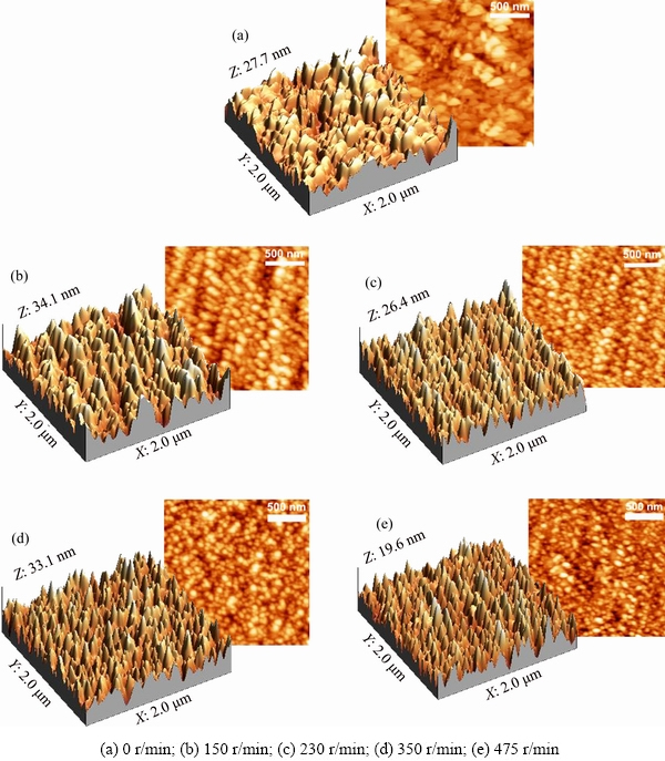
Fig. 2 AFM images of AZO thin films at different ��S
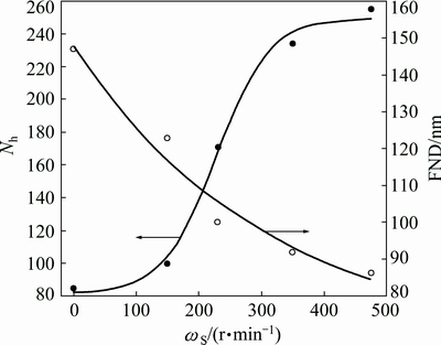
Fig. 3 Number of hills (Nh) and first neighbor distances (FND) at different substrate velocities
Figure 4 shows the XRD spectra for AZO thin films obtained for different ��S. The observed diffraction peaks for all samples correspond to the hexagonal wurtzite ZnO phase [22] with preferential orientation in the (002) plane, with the c-axis oriented preferentially normal to the substrate surface [23]. All peaks are shifted to the left in their (002) peak position with respect to the standard value of 34.467�� [22] which is evidence of tensile strain [24]. The other peak observed in the XRD patterns can be indexed to the (103) planes. In order to determine crystallite size of the AZO thin films, we considered the Scherrer��s formula [23], which is given by
 (1)
(1)
where D is the mean crystallite size, �� is the diffraction angle, �� is the FWHM and �� is the X-ray wavelength (0.15418 nm). The calculated crystallite sizes, D, of the samples were about 24.8, 27.7, 34.7, 31.3 and 29 nm, at ��S=0, 150, 230, 350 and 475 r/min, respectively, and these results are summarized in Table 1. There is clear evidence that all the AZO thin films grown under rotation presented larger crystallite sizes than those films grown on a stationary substrate, meaning that the substrate rotation improves the crystallinity of the thin films. The explanation for this improvement in crystallinity lies in the fact that the species that arrive to a rotating substrate have lower energy than to a stationary one. The time that the substrate spends in front of the target is reduced after increasing the substrate rotation speed. This causes an increasing of the collisions odds between the sputtered particles and the background gas molecules, thus reducing the energy of the sputtered species before reaching the substrate, favoring the energy for film growth, and this produces denser and (002) oriented thin films [18]. The lattice constants were calculated using the following equation [25]:
 (2)
(2)
where a and c are the lattice constants, and dhkl is the crystalline interplanar distance. Using the (002) diffraction peak, this equation becomes c=2dhkl.

Fig. 4 XRD patterns of AZO thin films prepared at different rotation velocities
Furthermore, we calculated the strain �� along the c-axis by [26]
 (3)
(3)
where c0 (0.52069 nm) is the unstrained c lattice parameter of ZnO. Strain and lattice parameter values are given in Table 1. Positive strain values correspond to tensile strain and negative values to compressive strain [26], which agrees with the shifting of the (002) diffraction peaks mentioned before.
Table 1 Characteristics of samples estimated from AFM and XRD data
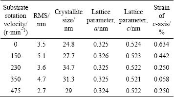
Figure 5 shows the FWHM value and the 2�� position for the (002) planes plotted against the substrate rotation velocity. As the rotation velocity increases, there is a decrement in the value of the FWHM, reaching its minimum for the sample grown at a substrate velocity of 230 r/min, which means that the substrate rotation improves the crystallinity of the thin films. Regarding the 2�� position for the (002) planes, it can be seen that all peak positions are shifted to lower values with respect to the standard value for ZnO and that there is a gradual increasing for the position of the 2�� as the substrate velocity increased, which means that the samples that were rotated had closer values to those of the standard which is 34.42�� [22]. As it was mentioned before, this is evidence of a positive strain, which in turn corresponds to a tensile strain. This suggests that the lattice parameters of the unit cell would show an increasing, which agrees with the reported lattice parameter values summarized in Table 1, in general larger than those of the standard ZnO (c0=0.52069 nm and a0=0.32495 nm). The explanation of this increment in the lattice parameters is as follows. There are two possible ways in which Al atoms are incorporated in the ZnO lattice, either in substitutional or interstitial sites. If Al3+ ions substitute Zn2+ ions, the lattice parameter in AZO samples would decrease and this would correspond to a shifting to the right (higher 2�� values) for the (002) peaks in comparison to the standard reported for the ZnO, due to the smaller radius of the Al3+ (0.054 nm) in comparison of the Zn2+ (0.074 nm). Furthermore, when Al atoms are incorporated into interstitial sites, the lattice parameter increases and this would correspond to a shifting to the left (lower 2�� values) for the (002) peaks [27]. This suggests that the Al atoms might mostly occupy interstitial sites in the case of the AZO thin films grown in this work. The reported �� values in Table 1 show that the samples grown using substrate rotation were under less tensile stress than the samples grown with no substrate rotation. This means that the crystallinity becomes better for thin films under substrate rotation. This is evidence that the crystallinity was greatly influenced by the substrate rotation favoring the formation of larger crystallite sizes which contributes to the reduction of the tensile stress contribution from crystalline boundaries [28]. These results confirm that the substrate rotation was effective in changing the structural properties of the AZO films. Based on the structural and morphological analysis, the optoelectronic performance is expected to be widely influenced by substrate rotation.
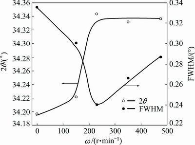
Fig. 5 Position of (002) peak and FWHM value at different substrate speeds
3.2 Optical properties
Figure 6 shows the transmission spectra of the samples obtained at different substrate speeds. It is possible to observe the oscillations in the high wavelength range due to optical interference, typical in very thin films. The average transmittance over the 400-800 nm range exceeds 90% regardless of the substrate rotation speed. We calculated the optical energy gap using the Tauc equations for all samples considering AZO as a direct band gap n-type semiconductor obtained from the (��hv)2 versus hv plot by extrapolating the linear portion of the curve to (hv=0) [29]. The bandgap values were 3.49, 3.67, 3.65, 3.61, 3.49 eV for the samples grown at ��S=0, 150, 230, 350 and 475 r/min, respectively. All bandgap values presented increased values respect of the standard ZnO, which is in the range of 3.20-3.40 eV. The higher band gap of the present AZO thin films compared with the bulk ZnO film could be attributed to the Burstein Moss effect [30]. The widening of the band gap was caused by the increasing of the free electron concentration after the doping with Al3+ ions; in degenerate semiconductors this causes an increasing of Fermi level, therefore optical band gap of doped zinc oxide is broader than that of undoped zinc oxide films [31].
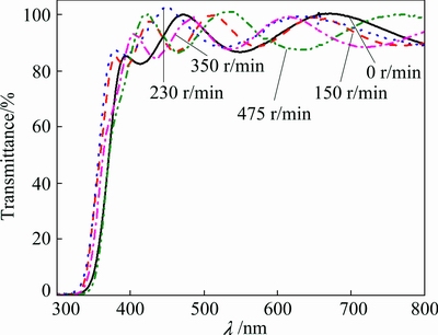
Fig. 6 Optical transmittance of AZO thin films
3.3 Electrical properties
The conduction mechanisms in ZnO are attributed to two main factors: the electrons generated from oxygen vacancies and the interstitial Zn atoms [32]. Due to the incorporation of Al3+ on substitutional sites of Zn2+ or Al atoms into interstitial sites, as well as oxygen vacancies and Zn interstitial atoms, the electrical conductivity in Al-doped ZnO thin films is expected to be higher than that in pure ZnO films [27]. The electrical properties of the deposited AZO thin films as a function of the substrate rotation speed are plotted in Fig. 7. All AZO thin films produced Hall voltages that indicated an n-type behavior. The experimental data revealed that as the substrate speed increases the resistivity also increases. The resistivity was increased from its minimum value of 8.5��10-3 ����cm at ��S=0 r/min to a maximum of 2.7��10-2 ����cm at ��S=350 r/min, while for all remaining samples the resistivity was in the order of 10-2 ����cm. Since �� is proportional to the reciprocal of the product of the carrier concentration ne and mobility ��H, the variations in resistivity with substrate rotation speed are attributed to the change in both ne and ��H. At 0 r/min, ne is about 1.8��1020 cm-3 with a Hall mobility of 4.19 cm2/(V��s) and remains in the order of 1020 cm-3 up to 230 r/min, with a Hall mobility of 3.50 cm2/(V��s). Then, ne rapidly decreases and reaches its lowest carrier value at ��S=350 r/min (1.29��1019 cm-3), with the highest value of Hall mobility (18.1 cm2/(V��s)), and then increases again to a value of 9.1��1019 cm-3, for ��S=475 r/min, with a Hall mobility of 3.23 cm2/(V��s). We speculate that since the grain size in the AZO thin films was decreased, the resistivity increased due to scattering with grain boundaries [33]. Also, the thin films grown under rotation had grains which were more uniform and denser than those presented in the sample grown using a stationary substrate. This type of microstructure contains fewer pores and projections, which act as traps for the free carriers and barriers for transporting the carriers in the films [34]. We suggest that the modification of the morphological and structural properties of the samples by rotating the substrate affected the Hall mobility and carrier concentrations, thus modifying the electrical conductivity. All of these results suggest that the substrate rotation plays an important role in the electrical properties of AZO thin films.
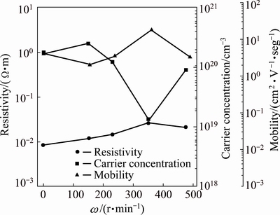
Fig. 7 Electrical properties of AZO thin films deposited at different substrate rotation velocities
4 Conclusions
AZO thin films were deposited at different substrate rotation rates by rf-magnetron sputtering on glass substrates. We applied several techniques such as scanning electron microscopy, X-ray diffraction, UV-Vis and the Van der Pauw technique to analyze the properties of the AZO thin films. Structural properties showed that all samples grew at a preferential orientation in the (002) plane direction and that the substrate rotation increased the crystallinity. Morphology results showed that substrate rotation produced highly defined nanostructures that became denser and sharper with ��S. All films presented a transmittance higher than 90% in the visible range, and the estimated optical energy gaps were in the range of 3.49-3.67 eV. The electrical properties showed that the lowest resistivity was achieved with a static substrate (8.5��10-3 ����cm), and that the substrate rotation induced changes in the carrier concentration and hall mobility which resulted in the increasing of electrical resistivity of the AZO thin films.
Acknowledgments
Authors thank Oswaldo  , Mario Herrera, Daniel Aguilar, Mauricio Romero, Dora Huerta, and Milenis Acosta
  for technical assistance and Lourdes Pinelo for secretary assistance. This work was supported by the Project No. CB/2012/178748 CONACYT/
  . One of the authors (A. IRIBARREN) thanks CONACYT/ under the program No. 260967 for sabbatical stances for Mexican and foreign researchers living abroad.
References
[1] CHANG S Y, HSIAO Y C, HUANG Y C. Preparation and mechanical properties of aluminum-doped zinc oxide transparent conducting films [J]. Surface and Coatings Technology, 2008, 202: 5416-5420.
[2] SHEN Hong-lie, ZHANG Hui, LU Lin-feng, JIANG Feng, YANG Chao. Preparation and properties of AZO thin films on different substrates [J]. Progress in Natural Science: Materials International, 2010, 20: 44-48.
[3] MONDAL S, BHATTACHARYYA S R, MITRA P. Effect of Al doping on microstructure and optical band gap of ZnO thin film synthesized by successive ion layer adsorption and reaction [J]. Pramana �C Journal of Physics, 2013, 80: 315-326.
[4] LEI Po-Hsun, HSU Chia-Ming, FAN Yu-Siang, YE Sheng-Jhang. Improved efficiency of InGaN/GaN light-emitting diodes with Al-doped zinc oxide using dual-plasma-enhanced metal-organic chemical vapour deposition system [J]. International Journal of Nanotechnology, 2014, 11: 359-372.
[5] LIU Chao-ying, XU Zhi-wei, ZHANG Yan-fang, FU Jing, ZANG Shu-guang, ZUO Yan. Effect of annealing temperature on properties of ZnO:Al thin films prepared by pulsed DC reactive magnetron sputtering [J]. Materials Letters, 2015, 139: 279-283.
[6] MORENO L,  C, BIZARRO M. Double-beam pulsed laser deposition for the growth of Al-incorporated ZnO thin films [J]. Applied Surface Science, 2014, 302: 46-51.
[7] MOHANTA A, SIMMONS J G, EVERITT H O, SHEN G, KIM S M, KUNG P. Effect of pressure and Al doping on structural and optical properties of ZnO nanowires synthesized by chemical vapor deposition [J]. Journal of Luminescence, 2014, 146: 470-474.
[8] SILVA T G, SILVEIRA E, RIBEIRO E, MACHADO K D, MATTOSO N,  I A. Structural and optical properties of ZnO films produced by a modified ultrasonic spray pyrolysis technique [J] . Thin Solid Films, 2014, 551: 13-18.
[9] KIM Young-Sung, TAI Weon-Pil. Electrical and optical properties of Al-doped ZnO thin films by sol�Cgel process [J]. Applied Surface Science, 2007, 253: 4911-4916.
[10]  J J, NARANJO F B. Radio frequency sputter deposition of high-quality conductive and transparent ZnO:Al films on polymer substrates for thin film solar cells applications [J].Thin Solid Films, 2009, 517: 3152-3156.
[11] JIANG Jin-long, WANG Qiong, HUANG Hao, WANG Yu-bao, ZHANG Xia, HAO Jun-ying. Microstructure and property changes induced by substrate rotation in titanium/silicon dual-doped a-C:H films deposited by mid-frequency magnetron sputtering [J]. Surface and Coatings Technology, 2014, 240: 419-424.
[12] SIYANAKI F H, DIZAJI H R, EHSANI M H, KHORRAMABADI S. The effect of substrate rotation rate on physical properties of cadmium telluride films prepared by a glancing angle deposition method [J].Thin Solid Films, 2015, 577: 128-133.
[13] CASTRO-RODRIGUEZ R, MENDEZ-GAMBOA J, PEREZ-QUINTANA I, MEDINA-EZQUIVEL R. CdS thin films growth by fast evaporation with substrate rotation [J]. Applied Surface Science, 2011: 9480-9484.
[14] PANICH N, SUN Y. Effect of substrate rotation on structure, hardness and adhesion of magnetron sputtered TiB2 coating on high speed steel [J]. Thin Solid Films, 2006, 500: 190-196.
[15] KIYOTAKA W. Handbook of sputter deposition technology: Principles, technology, and applications, noyes publications [M]. NJ, USA: Park Ridge, 1992.
[16] WADA K, YAMAGUCHI N, MATSUBARA H. Effect of substrate rotation on texture evolution in ZrO2-4 mol.% Y2O3 layers fabricated by EB-PVD [J]. Surface and Coatings Technology, 2005, 191: 367-374.
[17] JAYARAMAN V K, KUWABARA Y M,  de la luz Olvera Amador. Importance of substrate rotation speed on the growth of homogeneous ZnO thin films by reactive sputtering [J]. Materials Letters, 2016, 169: 1-4.
[18] SHI Qian, DAI Ming-jiang, LIN Song-sheng, HOU Hui-jun, WEI Chun-bei, HU Fang. Effect of sputtering conditions on growth and properties of ZnO:Al films [J]. Transactions of Nonferrous Metals Society of China, 2015, 25: 1517-1524.
[19] JUN Yeon-Sik, LEE Dong-Wook, JEON Duk-Young. Influence of dc magnetron sputtering parameters on surface morphology of indium tin oxide thin films [J]. Applied Surface Science, 2004, 221: 136-142.
[20] QIN Hua, WANG Li-gang, LIU Rui-jin, YUAN Wen-feng. Influence of target substrate distance on the properties of transparent conductive Si doped ZnO thin films [J]. Optik, 2014, 125: 3902-3907.
[21]  J M, COLCHERO J,
  J, BARO A M. WSXM: A software for scanning probe microscopy and a tool for nanotechnology [J]. Review of Scientific Instruments, 2007, 78: 013705-1-8.
[22] JCPDS-International Centre for Diffraction Data. PCPDFWIN v. 2.4. Chart No. 36-1451 [S]. 2003.
[23] LEE Ka-Eun, WANG Ming-song, KIM Eui-Jung, HAHN Sung-Hong. Structural, electrical and optical properties of sol�Cgel AZO thin films [J]. Current Applied Physics, 2009, 9: 683-687.
[24] KHORSAND ZAK A, ABD MAJID W H, ABRISHAMI M E, YOUSEFI R. X-ray analysis of ZnO nanoparticles by Williamson-Hall and size-strain plot methods [J]. Solid State Sciences, 2011, 13: 251-256.
[25] FANG G J, LI D J, YAO B L. Effect of vacuum annealing on the properties of transparent conductive AZO thin films prepared by DC magnetron sputtering [J]. Physica Status Solidi (A), 2002, 193: 139-152.
[26] GHOSH R, BASAK D, FUJIHARA S. Effect of substrate-induced strain on the structural, electrical, and optical properties of polycrystalline ZnO thin films [J]. Journal of Applied Physics, 2004, 96: 2689.
[27] PARK Ki-Cheol, MA Dae-Young, KIM Kun-Ho. The physical properties of Al-doped zinc oxide films prepared by RF magnetron sputtering [J]. Thin Solid Films,1997, 305: 201-209.
[28] YILDIZ A, CANSIZOGLU H, TURKOZ M, ABDULRAHMAN R, AL-HILO A, CANSIZOGLU M F, DEMIRKAN T M, KARABACAK T. Glancing angle deposited Al-doped ZnO nanostructures with different structural and optical properties [J]. Thin Solid Films, 2015, 589: 764-769.
[29] Al-GHAMDI A A, ALHUMMINAY H, ABDEL-WAHAB M S, YASHIA I S. Structure, optical constants and non-linear properties of high quality AZO nano-scale thin films [J]. Optik, 2016, 127: 4324-4328.
[30] GRILLI M L, SYTCHKOVA A, BOYCHEVA S, PIEGARI A. Transparent and conductive Al-doped ZnO films for solar cells applications [J]. Physica Status Solidi (A): Applications and Material Science, 2013, 210(4): 748-754.
[31] SUN Yi-hua, WANG Hai-lin, CHEN Jian, FANG Liang, WANG Lei. Structural and optoelectronic properties of AZO thin films prepared by RF magnetron sputtering at room temperature [J]. Transactions of Nonferrous Metals Society of China, 2016, 26: 1655-1662.
[32] IGASAKI Y, SAITO H. Substrate temperature dependence of electrical properties of ZnO:Al epitaxial films on sapphire (1210) [J]. Journal of Applied Physics, 1991, 69: 2190.
[33] MAYADAS A F, SHATZKES M. Electrical-resistivity model for polycrystalline films: The case of arbitrary reflection at external surfaces [J]. Physical Review B, 1970(1): 1382.
[34] LIU Y Y, YANG S Y, WEI G X, SONG H S, CHENG C F, XUE C S, YUAN Y Z. Electrical and optical properties dependence on evolution of roughness and thickness of Ga:ZnO films on rough quartz substrates [J]. Surface Coatings Technology, 2011, 205(11): 3530-3534.
������ת�ٶȶ���Ƶ���䷨�Ʊ�Al����ZnO��Ĥ�ṹ�����ܵ�Ӱ��
E. A. 1, L. G. DAZA1, A. J. R. 2, A. IRIBARREN1,3, R. CASTRO-RODRIGUEZ1
1. Departamento de Aplicada, CINVESTAV-IPN, Unidad , 97310, , ;
2. Institut et de l��Espace (ISAE), 10 Avenue Edouard Belin, 31000 Toulouse, France;
3. Instituto de Ciencia y de Materiales (IMRE), Universidad de La Habana, Zapata y G., Vedado, La Habana 10400, Cuba
ժ Ҫ��������Ƶ���䷨�������ڲ����������Ʊ���������ZnO(AZO)��Ĥ���о��˻�����ת�ٶ�(��S)�Ա�Ĥ��̬���ṹ����ѧ�͵�ѧ���ʵ�Ӱ�졣ɨ�������������ͼƬ��ʾ��ͨ��������ת�ܹ��������ܵ���״�ṹ��ԭ��������ͼ�������������ת״̬���γɵ���Ʒ���������Ȼ��徲ֹ״̬�µĿ���С�����ܣ��Ӷ�����ϸС�ľ����ߴ硣XRD������������б�Ĥ��Ϊ������п��ṹ��c������ȡ���ҷֲ�����Ӧ��������ɼ�����ƽ��������90%���ϡ�����S =0 r/minʱ�������ʴ������ֵ(8.5��10-3 ����cm)��������Ũ��Ϊ1.8��1020 cm-3������Ǩ����Ϊ4.19 cm2/(V��s)������������Ʒ��������ת������������Ũ�Ⱥͻ���Ǩ���ʵı仯���Ӷ����µ��������ӡ����������������ת�ٶȶ�AZO��Ĥ����ò���ṹ����ѧ�͵�ѧ���ܴ��ڽϴ�Ӱ�졣
�ؼ��ʣ�AZO��Ĥ����Ƶ�ſؽ��䣻���ṹ��������ܣ�������ת�ٶ�
(Edited by Bing YANG)
Corresponding author: E. A. ; Tel: +52-19999093681; E-mail: enrique.martin.tovar@gmail.com
DOI: 10.1016/S1003-6326(17)60230-9
Abstract: Al-doped ZnO (AZO) thin films were deposited on glass substrates by rf-sputtering at room temperature. The effects of substrate rotation speed (��S) on the morphological, structural, optical and electrical properties were investigated. SEM transversal images show that the substrate rotation produces dense columnar structures which were found to be better defined under substrate rotation. AFM images show that the surface particles of the samples formed under substrate rotation are smaller and denser than those of a stationary one, leading to smaller grain sizes. XRD results show that all films have hexagonal wurtzite structure and preferred c-axis orientation with a tensile stress along the c-axis. The average optical transmittance was above 90% in UV-Vis region. The lowest resistivity value (8.5��10-3 ����cm) was achieved at ��S=0 r/min, with a carrier concentration of 1.8��1020 cm-3, and a Hall mobility of 4.19 cm2/(V��s). For all other samples, the substrate rotation induced changes in the carrier concentration and Hall mobility which resulted in the increasing of electrical resistivity. These results indicate that the morphology, structure, optical and electrical properties of the AZO thin films are strongly affected by the substrate rotation speed.
