
Trans. Nonferrous Met. Soc. China 25(2015) 1176-1184
Effect of small changes in sintering temperature on varistor properties and degradation behavior of V-Mn-Nb-Gd co-doped zinc oxide ceramics
C. W. NAHM
Semiconductor Ceramics Laboratory, Department of Electrical Engineering, Dongeui University, Busan 614-714, Korea
Received 24 May 2014; accepted 8 October 2014
Abstract: The effect of small changes in sintering temperature on microstructure, electrical properties, dielectric characteristics, and degradation behavior of V-Mn-Nb-Gd co-doped zinc oxide ceramics was investigated. With the increase of sintering temperature, the densities of the sintered pellets decreased from 5.54 to 5.42 g/cm3 and the average grain size increased from 4.1 to 11.7 mm. The breakdown field (E1 mA) decreased noticeably from 7138 to 920 V/cm with the increase of sintering temperature. The varistor ceramics sintered at 900 ��C exhibited excellent nonohmic properties, which were 66 for the nonohmic coefficient and 77 mA/cm2 for the leakage current density. Concerning stability, the varistors sintered at 900 ��C exhibited the strongest accelerated degradation characteristics, with ��E1 mA =-9.2% for DC accelerated degradation stress of 0.85 E1 mA at 85 ��C for 24 h.
Key words: ZnO-V2O5-based ceramics; sintering; electrical properties; degradation behavior; varistor
1 Introduction
Essentially, semiconductor devices and IT systems are very susceptible or vulnerable to transient overvoltages such as electrostatic discharge (ESD), switching of electrical loads, magnetic and inductive coupling. Transient can originate from inside or outside a facility. However, the majority of surges are created within a facility. This is attributed to electrical circumstance that electronic systems are very complex and dense, because of a number of components and extremely narrow space between electric lines.
ZnO varistor ceramics are well known as a surge protection device (SPD) made by sintering ZnO powder modified with subordinate additives such as CoO, Sb2O3, MnO2, Cr2O3, together with Bi2O3 (or Pr6O11) as main additives [1-5]. Electrically, they exhibit symmetric V-I characteristics similar to a back-to-back Zener diode having a single junction [1-3]. Microstructually, they are featured by multi-junctions composed of grain and grain boundaries, which are distributed three-dimensionally through sintered ceramics.
Commercial multilayered chip varistor (MLV) ceramics are based on Bi2O3 and Pr6O11 as a varistor- former. ZnO ceramics added with Bi2O3 and Pr6O11 require a high sintering temperature and consequently have no choice but to use a refractory related to Pd or Pt as an inner-electrode. New ZnO ceramics added with V2O5 as a varistor-former have an important advantage, which can use much cheaper Ag, when compared with Pd or Pt [6,7]. Until now, a study on ZnO-V2O5-based ceramics has been investigated in many points: microstructure, electrical properties, dielectric characteristics, and degradation behavior according to experimental variables such as additives and sintering process [8-18]. However, yet there are many problems to be solved in order to use commercially. The sintering process for specific composition can improve nonohmic properties in the ZnO-V2O5 ceramics [11,12,14-18]. Therefore, it is very interesting to investigate how the sintering process affects varistor properties for specific composition. In this work, sintering temperature dependence on microstructure, nonohmic properties, dielectric characteristics, and DC-degradation behavior of the V-Mn-Nb-Gd co-doped zinc oxide ceramics was investigated at low temperatures of 875, 900, 925, and 950 ��C, respectively. A surprisingly high nonohmic coefficient and high stability were attained by a proper sintering process.
2 Experimental
High-purity (>99.9%) reagent-grade raw materials composed of 97.35% ZnO (mole fraction, Aldrich Chemical Co., USA), 0.5% V2O5 (Kojundo Chemical Laboratory, Japan), 2.0% MnO2 (Kojundo Chemical Laboratory, Japan), 0.1% Nb2O5 (Kojundo Chemical Laboratory, Japan), 0.05% Gd2O3 (Kojundo Chemical Laboratory, Japan) were prepared. Raw materials were mixed by ball milling with zirconia balls and acetone in a polypropylene bottle for 24 h. The mixture was dried at 120 ��C for 12 h. The dried mixture was put into container with acetone and 0.8% polyvinyl butyral (PVB, mass fraction) binder of powder. After drying, the mixture was granulated by sieving through a screen with a pore diameter of 0.15 mm to produce the starting powder. The sieved powder was pressed into disk-shaped pellets of 10 mm in diameter and 1.5 mm in thickness at a pressure of 100 MPa. The pellets were set on MgO plate and sintered at different temperatures (875, 900, 925 and 950 ��C) in air for 3 h, and furnace-cooled to room temperature. The heating and cooling rates were 4 ��C/min. The final pellets were roughly 8 mm in diameter and 1.0 mm in thickness. Conductive silver paste was coated by screen-printing techniques on both faces of the pellets and the electrodes were formed by heating it at 550 ��C for 10 min. The electrodes were 5 mm in diameter. Finally, after soldering the lead wire to both electrodes, the samples were packaged by dipping them into a thermoplastic resin powder.
One side of the samples was lapped and ground with SiC paper, and then polished with 0.3 ��m-Al2O3 powder to a mirror-like surface. The polished samples were chemically etched in HClO4-H2O solution (1:1000, volume ratio) at 25 ��C for 25 s. The surface microstructure was examined by a field emission scanning electron microscope (FESEM, Quanta 200, FEI, Brno, Czech). The average grain size (d) was determined by the linear intercept method [19]. The crystalline phases were identified by X-ray diffractometer (XRD, X'pert-PRO MPD, Panalytical, Almelo, Netherlands) with Cu K�� radiation. The density (r) of the sintered pellet was measured using a density determination kit (238490) attached to balance (AG 245, Mettler Toledo International Inc., Greifensee, Switzerland).
The electric field (E)-current density (J) characteristics were measured using a high voltage source-measure unit (Keithley 237, Keithley Instruments Inc., Cleveland, OH, USA). The breakdown field (E1 mA) was measured at a current density of 1.0 mA/cm2 and the leakage current density (JL) was measured at 0.80E1 mA. The nonohmic coefficient (��) was determined through the expression, ��=(lg J2-lg J1)/(lg E2-lg E1), where E1 and E2 are the electric fields corresponding to J1=1.0 mA/cm2 and J2=10 mA/cm2, respectively. The dielectric behavior in accordance with frequency for the apparent dielectric constant (�š�APP) and dissipation factor (tan ��) of the samples was measured in the range of 100 Hz-2 MHz using an RLC meter (QuadTech 7600, Marlborough, MA, USA).
The DC-accelerated degradation test was performed for stress state of 0.85E1 mA at 85 ��C for 24 h. Simultaneously, the leakage current was monitored at intervals of 1 min during stressing using a high voltage source-measure unit (Keithley 237, Keithley Instruments Inc., Cleveland, OH, USA). The degradation rate coefficient (KT) was calculated through the expression IL=IL0+KTt1/2, where IL is the leakage current at stress time (t) and IL0 is IL at t=0 [20]. After application of a stress, the E-J characteristics were measured at room temperature.
3 Results and discussion
Figure 1 shows the SEM micrographs of the samples sintered at different temperatures. Outwardly, firstly a remarkable difference cannot be found when compared with the surface morphologies of other ZnO-V2O5-based varistor ceramics, and secondarily the grain size changes greatly despite small changes in the sintering temperature, in particular, exceeding 925 ��C. Finally, it can be seen that the pores exist at the grain boundaries. The microstructure characteristic parameters are summarized in Table 1. The average grain size increased remarkably in the range of 4.1-11.7 ��m in spite of small sintering changes with the increase of sintering temperature. The density of sintered pellets decreased from 5.54 to 5.42 g/cm3 corresponding to 95.8%-93.8% of the theoretical density (��TD) (pure ZnO, ��TD=5.78 g/cm3) with the increase of sintering temperature. This is attributed to the volatility of the V-species for V2O5 with low melting point as low as 690 ��C.
The XRD patterns of the samples at different sintering temperatures are shown in Fig. 2. These patterns revealed the presence of Zn3(VO4)2, ZnV2O4, GdVO4, and VO2 as minor secondary phases. Among minor phases, ZnV2O4 (2q=30.0789��, 35.4033��) and VO2 (2q=28.0650��) almost disappeared when the sintering temperature exceeded 925 ��C. It is assumed that this is related to the volatility of liquid phase when the sintering temperature exceeds 925 ��C. The disappearance of ZnV2O4 and VO2 may affect nonohmic properties. In contrast, no GdVO4 was affected by sintering temperature.
Figure 3 shows the electric field-current density (E-J) characteristics of the samples sintered at different temperatures. The varistor properties are featured by the nonohmicity in the E-J relation. The characteristic curves are composed of two states: one is current-off state before breakdown field, the other is current-on state after breakdown field. However, the shape of edge between ohmic region and nonohmic region shows an obvious difference with sintering temperature. The E-J characteristic parameters obtained from E-J curves are summarized in Table 1.
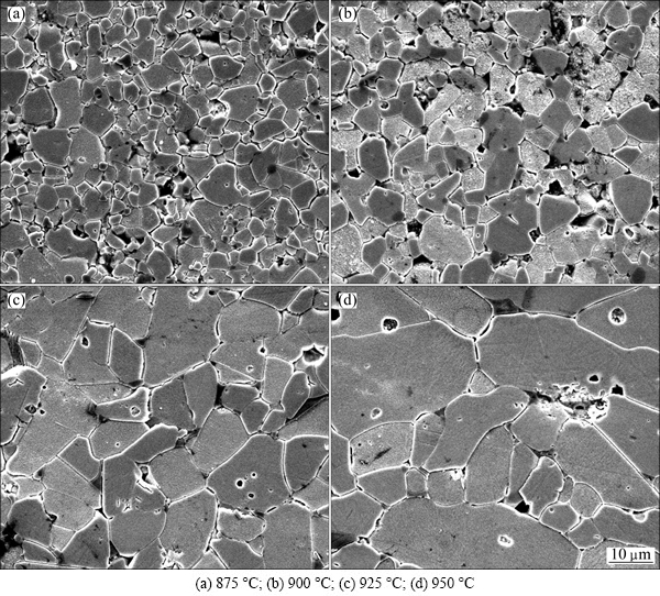
Fig. 1 SEM micrographs of samples sintered at different temperatures
Table 1 Average grain size, sintered density, electrical and dielectric parameters of samples sintered at different temperatures
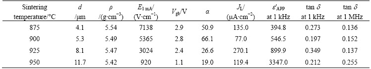
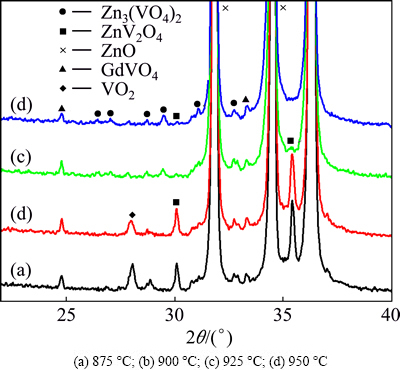
Fig. 2 XRD patterns of samples sintered at different temperatures
Figure 4 shows grain size, sintered density and electrical and dielectric parameters of the samples sintered at different temperatures. The behavior of breakdown field (E1 mA) as a function of sintering temperature is indicated graphically in Fig. 4(c). The E1 mA decreased abruptly from 7138 to 920 V/cm despite small sintering changes with the increase of sintering temperature. The E1 mA is predominantly controlled by the grain size (d), and slightly depends on the breakdown voltage per grain boundaries (Vgb). The breakdown voltage (VB) is indicated as: VB=(D/d)Vgb=nVgb, furthermore, E1 mA is written as E1 mA=Vgb/d, where D is the thickness of sample, and n is the number of grain boundaries [1,3]. Therefore, VB is proportional to n and Vgb. In general, to control the breakdown voltage, one is to control the sample thickness at the fixed grain size, the other is to control the grain size at the constant sample thickness. As a result, the decrease of E1 mA with the increase of sintering temperature is attributed to the increase of the average ZnO grain size and the decrease of breakdown voltage per grain boundary.
Fig. 3 E-J characteristics of samples sintered at different temperatures
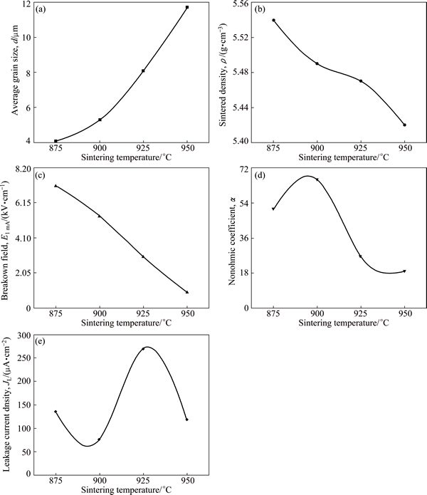
Fig. 4 Average grain size (a), sintered density (b) and E-J parameters (c-e) of samples as function of sintering temperature
The behavior of nonohmic coefficient (��) as a function of sintering temperature is indicated graphically in Fig. 4(d). The �� value increased from 51 to 66 when the sintering temperature was increased from 875 to 900 ��C and then decreased to 19 when the sintering temperature was further increased from 900 to 950 ��C. In the light of changing tendency, it can be seen that the sintering temperature in this system has a strong effect on nonohmic properties in spite of small sintering changes. It should be emphasized that the sample sintered at a temperature as low as 900 ��C exhibited the highest value (��=66), when compared with other varistors reported until now [15-17]. In addition, it is worth noting that the sample sintered at a temperature as low as 875 ��C exhibited a high �� value, reaching ��=51. However, �� value abruptly decreased less than 30 when the sintering temperature exceeded 925 ��C. The behavior of �� with sintering temperature is related to the potential barrier height, which strongly depends on the electronic trap states, such as the zinc vacancies, interstitial zinc, ionized donor-like and oxygen at the grain boundaries. Furthermore, these defects will vary the density of interface states at the grain boundaries. Based on XRD analysis, it is assumed that the disappearance of ZnV2O4 and VO2 will change the density of interface states when the sintering temperature exceeds 925 ��C, in the light of the decrease of nonohmic coefficient.
The behavior of leakage current density (JL) as a function of sintering temperature is indicated graphically in Fig. 4(e). The JL value decreased from 135 to 77 mA/cm2 with the increase of sintering temperature up to 900 ��C. Thereafter it increased up to 925��C and again decreased up to 950 ��C. Therefore, it was found to have a fluctuation with the increase of sintering temperature.
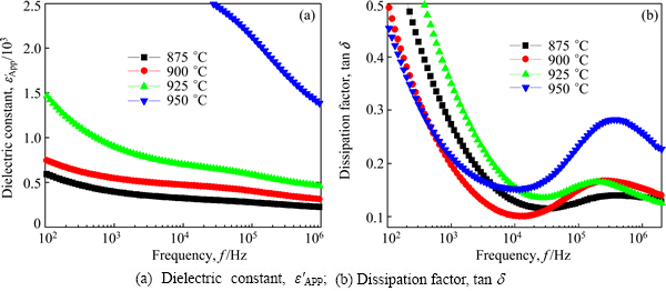
Fig. 5 Dielectric characteristics of samples vs frequency at different sintering temperatures
Figure 5 shows the apparent dielectric constant (�š�APP) and dissipation factor (tan ��) of the samples sintered at different temperatures. The behavior of �š�APP for all samples showed the dielectric dispersion phenomena, which decreased with an increase in the frequency. The decrease of �š�APP with increasing frequency is attributed to the decrease of the number of dipole, which can follow to test frequency. In particular, the dielectric dispersion for all samples in common was large at below 1 kHz and above 100 kHz. In addition, the dielectric dispersion increased with the increase of sintering temperature. The �š�APP increased with the increase of sintering temperature in the range of overall frequency. On the other hand, tan �� decreased abruptly until the vicinity of roughly 10 kHz with increasing frequency and exhibited a dielectric absorption peak in the vicinity of 200-300 kHz, and thereafter again decreased. The detailed dielectric characteristic parameters are summarized in Table 1.
The behavior of �š�APP at 1 kHz as a function of sintering temperature is indicated graphically in Fig. 6(a). The �š�APP increased from 394.8 to 3347.0 with the increase of sintering temperature from 875 to 950 ��C. This is directly related to the average grain size and depletion layer width, as can be seen in the following expression: �š�APP=��g(d/t), where ��g is the dielectric constant of ZnO (8.5), d is the average grain size, and t is the depletion layer width of the both sides at the grain boundaries. The behavior of tan �� at 1 kHz as a function of sintering temperature is indicated graphically in Fig. 6(b). The tan �� at 1 kHz was found to have a fluctuation with the increase of sintering temperature. The sample sintered at 900 ��C exhibited the lowest value (0.197) in the tan �� at 1 kHz. On the whole, the changing tendency of tan �� was similar to that of leakage current in accordance with sintering temperature. However, the behavior of tan �� at 1 MHz is entirely different from that at 1 kHz. At present, it is assumed that this is attributed to the dipolar rotation with frequency.
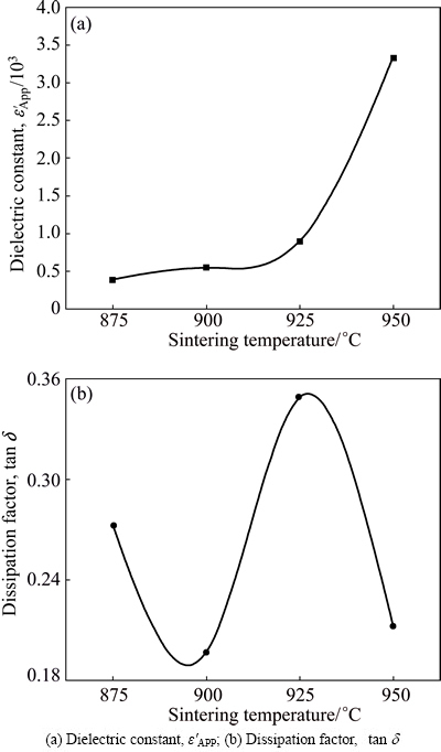
Fig. 6 Dielectric parameters as function of sintering temperature
Figure 7 shows the behavior of leakage current (IL) during DC accelerated degradation stress of 0.85 E1 mA at 85 ��C for 24 h for the samples sintered at different temperatures. Obviously, it can be seen that the sintering temperature has a noticeable effect on the behavior of IL for applying the stress. The sample sintered at 875 ��C exhibited the thermal runaway in a few seconds for applying the stress. In general, the density of the sintered pellet and the leakage current greatly have a significant effect on the stability. The low sintered density decreased the number of conduction path and eventually led to the concentration of current. The high leakage current led to repetition cycle between joule heating and leakage current. Although the samples sintered at 875 ��C exhibited relatively high sintered density, they seemed to exhibit extremely low stability due to much higher leakage current. The sample sintered at 925 ��C exhibited a positive creep of leakage current (PCLC), in which the IL abruptly increased with the increase of the stress time. The stability of the samples can be estimated by the degradation rate coefficient (KT), indicating the degree of degradation. This is the slope of leakage current for the stress time and lower KT leads to higher stability. As a result, the KT value of the samples sintered at 925 ��C was 103.2 ��A��h-1/2. In contrast, the samples sintered at 900 and 950 ��C exhibited weak PCLC, in which IL gradually increased with the increase of the stress time. They showed a good stability, which exhibited 19.6 and 13.3 ��A��h-1/2 in KT, respectively. The behavior of IL with the stress in these samples is obviously different from that of Zn-V-Mn-Nb (ZVMN) varistors modified with Er2O3 and Bi2O3 [16,17].
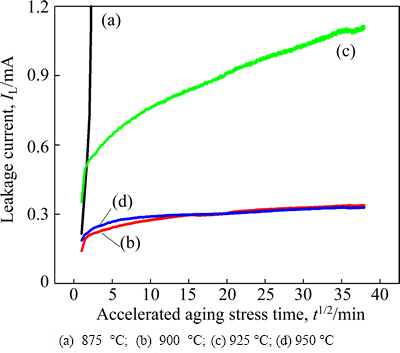
Fig. 7 Leakage current behavior during stress of samples sintered at different temperatures
Figure 8 shows the effect of sintering temperature of E-J characteristics before and after application of a stress of the samples sintered at different temperatures. It can be seen that the sintering temperature has a significant effect on E-J curves after application of a stress. The sample sintered at 875 ��C exhibited a large variation in the E-J characteristics because of thermal runaway after application of a stress. This sample lost almost nonohmic properties. Next, the sample sintered at 925 ��C exhibited a large difference, when compared with initial E-J characteristics curve. Also this sample showed a weak stability against the stress. The sample sintered at 950 ��C exhibited a significant variation in the vicinity of the knee. The sample sintered at 900 ��C exhibited the smallest variation of E-J characteristics, when compared with other samples after application of a stress. However, this sample also accompanied small variation in the vicinity of knee. The variations of E-J characteristic parameters before and after application of a stress of the samples sintered at different temperatures are summarized in Table 2. The behavior of E1 mA and �� after application of a stress with initial E1 mA and �� for the samples sintered at different temperatures is indicated graphically in Fig. 9. The variation rate in E1 mA after application of a stress increased in the order of 900��950��925��950 ��C. Only the sample sintered at 900 ��C exhibited the DE1 mA less than 10% after application of a stress. On the other hand, �� after applying the stress greatly changed unlike E1 mA. All samples except for the sample sintered at 900 ��C decreased considerably less than 10 in the nonohmic coefficient after application of a stress. However, the sample sintered at 900 ��C exhibited the nonohmic coefficient more than 20 after applying the stress. On the whole, also, the JL value increased extremely after application of a stress unlike E1 mA and ��.
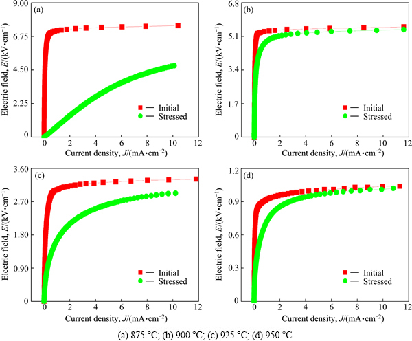
Fig. 8 E-J characteristic behavior before and after application of stress of samples sintered at different temperatures
Table 2 E-J characteristic parameters of samples sintered at different temperatures before and after application of stress
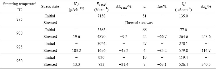
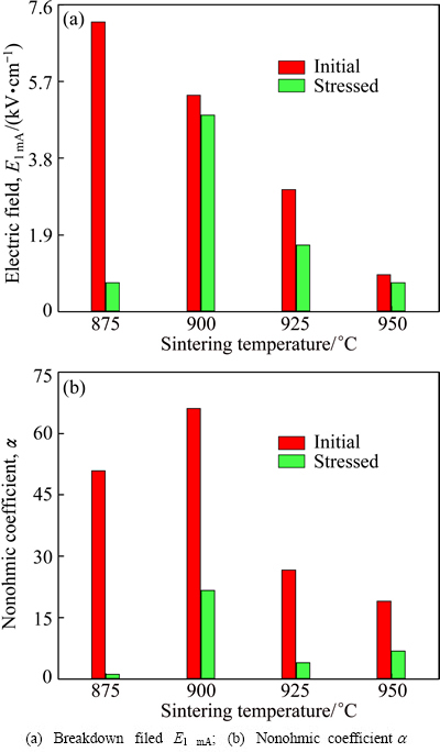
Fig. 9 E-J characteristic parameters before and after application of stress of samples sintered at different temperatures
4 Conclusions
The microstructure, electrical properties, dielectric characteristics, and degradation behavior of V-Mn-Nb- Gd co-doped zinc oxide ceramics were systematically investigated for the samples sintered at different temperatures. Increasing sintering temperature yielded the decrease in the sintered density and the increase in the average grain size. The breakdown field decreased with the increase of sintering temperature. The varistor ceramics sintered at 900 ��C exhibited excellent nonohmic properties, with a high nonohmic coefficient (��=66). Furthermore, the varistor ceramics sintered at 900 ��C exhibited the highest stability, with ��E1 mA= -9.2% for DC accelerated degradation stress of 0.85E1 mA at 85 ��C for 24 h.
References
[1] LEVINSON L M, PILIPP H R. Zinc oxide varistor��A review [J]. American Ceramic Society Bulletin, 1986, 65: 639-646.
[2] MUKAE K. Zinc oxide varistors with praseodymium oxide [J]. American Ceramic Society Bulletin, 1987, 66: 1329-1331.
[3] GUPTA T K. Application of zinc oxide varistor [J]. Journal of the American Ceramic Society 1990, 73: 1817-1840.
[4] CHEN G H, LI J L, YANG Y, YUAN C L, ZHOU C R. Microstructure and electrical properties of Dy2O3-doped ZnO�CBi2O3 based varistor ceramics [J]. Materials Research Bulletin, 2014, 50: 141-147.
[5] NAHM C W. The nonlinear properties and stability of ZnO-Pr6O11-CoO-Cr2O3-Er2O3 ceramic varistors [J]. Materials Letters, 2001, 47: 182-187.
[6] TSAI J K, WU T B. Non-ohmic characteristics of ZnO-V2O5 ceramics [J]. Journal of Applied Physics, 1994, 76: 4817-4822.
[7] TSAI J K, WU T B. Microstructure and nonohmic properties of binary ZnO-V2O5 ceramics sintered at 900 ��C [J]. Materials Letters, 1996, 26: 199-203.
[8] HNG H H, KNOWLES K M. Knowles, microstructure and current�Cvoltage characteristics of multicomponent vanadium-doped zinc oxide varistors [J]. Journal of the American Ceramic Society, 2000, 83: 2455-2462.
[9] HNG H H, CHAN P L. Effects of MnO2 doping in V2O5-doped ZnO varistor system [J]. Materials Chemistry Physics, 2002, 75: 61-66.
[10] CHEN C S. Effect of dopant valence state of Mn-ions on the microstructures and nonlinear properties of microwave sintered ZnO-V2O5 varistors [J]. Journal of Materials Science, 2003, 38: 1033-1038.
[11] NAHM C W. DC accelerated aging behavior of Co-Dy-Nb doped Zn-V-M-based varistors with sintering process [J]. Journal of Materials Science: Materials in Electronics, 2011, 22: 444-451.
[12] NAHM C W. Sintering effect on pulse aging behavior of Zn-V-Mn-Co-Dy-Nb varistors [J]. Journal of the American Ceramic Society, 2011, 94: 2269-2272.
[13] MING Z, YU S, SHENG T C. Grain growth of ZnO-V2O5 based varistor ceramics with different antimony dopants [J]. Journal of the European Ceramic Society, 2011, 31: 2331-2337.
[14] NAHM C W. Effect of sintering process on electrical properties and ageing behavior of ZnO-V2O5-MnO2-Nb2O5 varistor ceramics [J]. Journal of Materials Science: Materials in Electronics, 2012, 23: 457-463.
[15] NAHM C W. Major effects on electrical properties of ZnO-V2O5-MnO2-Nb2O5-Er2O3 ceramics with sintering changes [J]. Ceramics International, 2012, 38: 2593-2596.
[16] NAHM C W. Effect of sintering temperature on electrical properties, dielectric characteristics, and aging behavior of ZnO-V2O5-based varistor ceramics modified with Bi2O3 [J]. Journal of Materials Science: Materials in Electronics, 2013, 24: 118-124.
[17] NAHM C W. Improvement of aging characteristics of (Mn, Nb, Er)-doped ZnO-V2O5-based varistor ceramics by small sintering changes [J]. Journal of Materials Science: Materials in Electronics, 2013, 24: 2228-2233.
[18] MIRZAYI M, HEKMATSHOAR M H. Effect of V2O5 on electrical and microstructural properties of ZnO ceramics [J]. Physica B, 2013, 414: 50-55.
[19] WURST J C, NELSON J A. Lineal intercept technique for measuring grain size in two-phase polycrystalline ceramics [J]. Journal of the American Ceramic Society, 1972, 55: 109-111.
[20] FAN J, FREER R. Deep level transient spectroscopy of zinc oxide varistors doped with aluminum oxide and/or silver oxide [J]. Journal of the American Ceramic Society, 1994, 77: 2663-2668.
�ս��¶ȵ�ϸ�仯��V-Mn-Nb-Gd����������п�մ�ѹ�����Ժ�˥����Ϊ��Ӱ��
C. W. NAHM
Semiconductor Ceramics Laboratory, Department of Electrical Engineering, Dongeui University, Busan 614-714, Korea
ժ Ҫ��
�о��ս��¶ȵ�ϸ�仯��V-Mn-Nb-Gd����������п�մ�����֯�������ܡ�������ܺ�˥����Ϊ��Ӱ�졣�����ս��¶ȵ����ߣ��ս������ܶ���5.54 g/cm3���͵�5.42 g/cm3��ƽ�������ߴ���4.1 ��m������11.7 ��m��������ǿ��7138 V/cm���罵����920 V/cm����900 ��C�ս��ѹ���մɳ��ּ��ѵķ�����(��ŷķ)���ԣ��������ϵ����©�����ܶȷֱ�Ϊ66��77 ��A/cm2���������ȶ��Է��棬��85 ��C��24 h��0.85E1 mA��ֱ������Ӧ���£���900 ��C�ս��ѹ���մɳ�����ǿ�ļ���˥�����ԣ����䦤E1 mA=-9.2%��
�ؼ��ʣ�
ZnO-V2O5���մ����ս�����������˥����Ϊ��ѹ����������
(Edited by Wei-ping CHEN)
Corresponding author: C. W. NAHM; Tel: +82-51-890-1669; Fax: +82-51-890-1664; E-mail: cwnahm@deu.ac.kr
DOI: 10.1016/S1003-6326(15)63713-X
ժ Ҫ���о��ս��¶ȵ�ϸ�仯��V-Mn-Nb-Gd����������п�մ�����֯�������ܡ�������ܺ�˥����Ϊ��Ӱ�졣�����ս��¶ȵ����ߣ��ս������ܶ���5.54 g/cm3���͵�5.42 g/cm3��ƽ�������ߴ���4.1 ��m������11.7 ��m��������ǿ��7138 V/cm���罵����920 V/cm����900 ��C�ս��ѹ���մɳ��ּ��ѵķ�����(��ŷķ)���ԣ��������ϵ����©�����ܶȷֱ�Ϊ66��77 ��A/cm2���������ȶ��Է��棬��85 ��C��24 h��0.85E1 mA��ֱ������Ӧ���£���900 ��C�ս��ѹ���մɳ�����ǿ�ļ���˥�����ԣ����䦤E1 mA=-9.2%��
