
Ge+ע��Si1-xGex/Si���ʽ���˻���Ϊ
������1, ����2, ������3
(1. ���ϴ�ѧ ������ѧ�뼼��ѧԺ,���� ��ɳ,410083;
2. ���ϴ�ѧ ���Ͽ�ѧѧԺ,���� ��ɳ,410082;
3. ���ϴ�ѧ ��ĩұ���о�Ժ,���� ��ɳ,410083)
ժҪ: ��ע������Ϊ100 keVʱ,��ע�����Ϊ5.3��1016/cm2��Ge+ע��(001)SIMOX��Ĥ���Ʊ�Si1-xGex/Si���ʽ�;Ȼ��,����Ʒ���е��ٵƿ������˻�,�˻��¶�Ϊ700~1050 ��,�˻�ʱ��Ϊ5~30 min������Ʒ��(004)��(113)��X�����������ݽ��м���ͷ���,�ó��˻��¶�Ϊ1000 �桢�˻�ʱ��Ϊ30 minΪ����˻��������ڴ��˻�������,���������������Ϊ�;�����,90%��ע��Ge+λ�����λ��,��ͬʱ����Ӧ���ԥ,��λ�����λ�õ�Ge+�ﵽ�������ֵ��82%,��������Ϊ0.438�����ڸ���Ge+ע��������澧�����������Լ�Ӧ���ԥ�ͷŵ�λ����ȱ��,���,����ᾧ������̫���롣
�ؼ���: ����ע��; Si1-xGex/Si���ʽ�; �˻���Ϊ; X��������
��ͼ�����:TN305.3 ���ױ�ʶ��:A ���±��: 1672-7207(2005)04-0560-06
Annealing behavior of Si1-xGex/Si heterostructureformed by Ge+ implantation with X-ray diffraction
LUO Yi-min1, CHEN Zhen-hua2, HUANG Pei-yun3
(1. School of Physics Science and Technology, Central South University, Changsha 410083, China;
2. School of Materials Science, Hunan University, Changsha 410082, China;
3. Institute of Powder Metallurgy, Central South University, Changsha 410083, China)
Abstract: Si1-xGex/Si heterostructure was prepared by implanting 5.3��1016/cm2 of Ge+ into (001) separation by implanted oxygen(SIMOX) wafers of silicon at 100 keV and annealed at 700-1050 �� for 5-30 min. The X-ray diffraction data of crystal planes (004) and (113) of samples show that good annealing effect may be attained at 1000 �� for 30 min. If we assume that solid phase growth epitaxial (SPEG) is pseudomorphic growth, and 90% of implanted Ge+ is situated in the substitution site, this percentage is corrected to 82% of theoretical value when considering strain relaxation, and the coherent factor is 0.438. The quality of crystallized film is not perfect enough owing to the serious damage of crystal lattice produced by a high dose of Ge+ implantation and dislocation and defect released by strain relaxation.
Key words: ion implantation; Si1-xGex/Si heterostructure; annealing behavior; X-ray diffraction
Si1-xGex���ʽ��Լ��ڴ˻����Ϸ�չ������[CM(22] ����������,�ڹ������������������ʮ����Ҫ��Ӧ��[1]��������Si���ϵ�SiGe�Ͻ����������������������������źܴ��Ӧ��DZ��[2-4];SiGe������ЧӦ�������ͬ��Si���������ʾ���ϸߵĿ�ѨǨ���ʺͿ絼[5];��SiGeΪ����˫�������(HBT)���нϸߵĵ������������[2,3,6]����Si1-xGex���ʽ���,���ܴ��Ľ������ȿ���Ge�����ı�[7],�䳬�����ڵij���������Brillouin���۵�ЧӦ������䵼���ܹ��ڲ�ʸ�ռ��ƶ�,ʹ֮��Ϊֱ����϶����[8],�˷����ʰ뵼����ϼ����϶������,ʹ��Si�����ɵ����ġ����ʹ��̡����롰�ܴ����̡��Ρ��ϳ�SiGe���ʽ�ķ����ܶ�,��Ҫ�з��������ӷ�[9,10],������ջ�ѧ���������������ע�뷨[11]�ȡ�����ע�뷨�ǽ�Ge+ע��赥�������ÿ������˻������������(SPEG)�γ�SiGe�Ͻ�㡣�������������,����ע����кܴ����Խ��,��Ϊ����Si���ɵ�·��������,������Լ�,����Ч�ʸ�[12-15]��
X���������ѱ��㷺Ӧ����Si1-xGex���ʽ���о�[16]���ڴ�,��������ͨ���Ը���Ge+ע��Si���������˻��õ�Si1-xGex��Ĥ��X�����������ķ���,�ó�λ�����λ�õ�Ge��������ӳӦ���ԥ���ԵĹ������ӵ���Ҫ����,�����˻���Ʒ�ı���ᾧ�������ж��Է�����
1 ʵ����
��ʵ��������Ʒ��ͼ1��ʾ��363.3 nm���SiO2�����ͨ������SIMOX�����õ����봫ͳ��SOI�������,SIMOX�кܶ��ŵ�[1,17]��Ge+��ֱ�ھ���(001)ע��,ע������Ϊ100 keV,ע�����Ϊ5.3��1016/cm2������TRIM90 Code,ͶӰ���RpΪ71.1 nm,ƽ��������릤Rp=21.2 nm��������÷�ֵGe+Ũ�ȵ�����ֵΪ0.998��1022/cm3,ԭ��������xmΪ19.96%[18]��
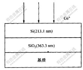
ͼ 1 ע����Ʒʾ��ͼ
Fig. 1 Diagram of implanted sample
��Ʒ����õ��ٵƿ������˻�,�˻��ڼ�䵪������,�˻���������1��
�� 1 ��Ʒ�˻�����
Table 1 Annealing conditions of samples

ͼ2��ͼ3��ʾΪGe+ע����Ʒ����ͬ�¶�,��ͬʱ���˻���X��������ͼ�ס�����,ͼ2��ʾΪ1�š�2�š�3�ź�4����Ʒ��Si������(004)��X��������ͼ��,ͼ3��ʾΪ4�š�5�ź�6����Ʒ��(004)��X��������ͼ�ס�
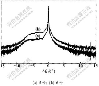
ͼ4��ͼ5��ʾΪ5�ź�6����Ʒ��(113)��X��������ͼ�ס�ͼ6��ʾ��ΪX����С�������С�dz����·ʾ��ͼ������:��Ϊ�������뷴���� [CM(22] (113)�ļн�;��Ϊ������(113)����Ʒƽ��(001)��
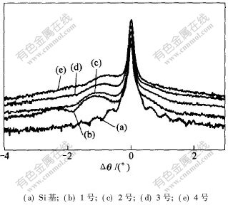
ͼ 2 ��ͬ�˻���������Ʒ��(004)��X��������ͼ��
Fig. 2 X-ray diffraction patterns on plane (004) of samples annealed in different conditions
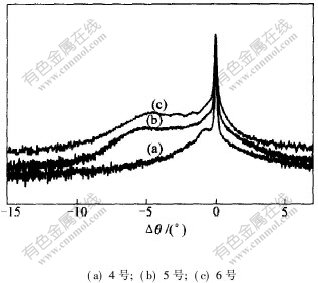
ͼ 3 ��һ���˻����Ʒ��(004)��X��������ͼ��
Fig. 3 X-ray diffraction patterns on plane(004) of samples after further annealing
ͼ 4 ��Ʒ��(113)��С������X��������ͼ��
Fig. 4 X-ray diffraction patterns on plane (113)of samples under small angle incidence
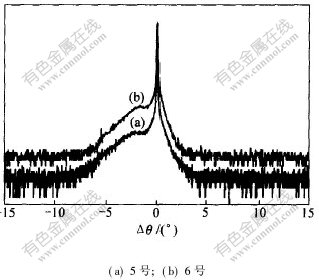
ͼ 5 ��Ʒ��(113)��С�dz���X��������ͼ��
Fig. 5 X-ray diffraction patterns on plane(113) of samples under small angle exit
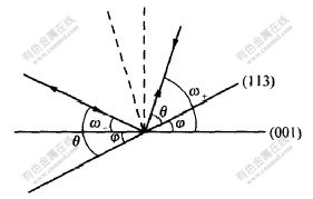
ͼ 6 (113)��С�������С�dz���ʾ��ͼ
Fig. 6 Diagram of small angle incidence and small angle exit on plane (113) of samples under small angle incidence
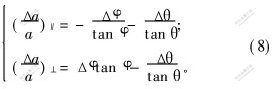
�н�;��-�ͦ�+��ֱ�ΪС�������С�dz���ʱ����������Ʒƽ��ļнǡ���ͼ�ɼ�,�����й�ϵʽ����:
![]()
2 ��������
2.1 Ge+Ũ�ȵļ���
���ݽ���ѧ����,(hkl)����������Ϊ:
![]()
δע��Ge+�ĵ�����,����Ϊ��������,��a=b=c;Ge+ע���,�����������仯,����������������״��
���������X��������ͼ�õ�,���ݲ�����ʽ:
![]()
��֪,����Ge�ľ���������Si�ľ�����,Ge+ע���������Ӧ����,���һ�������(��B)����С,��ӳ��X��������ͼ����,���Ƿ彫����ڳĵ������ƶ�,�ƶ��ľ���������ĸı����й�,���Ҳ��Ge�����йء�
��
![]()
����:��Ϊ������ĵ������ֵ,����Ϊ���Ƿ���ĵ��ľ���,��ͨ�������õ���
��
![]()
��ʽ(6)�ɵ�ע��Ge+��Si1-xGex�Ͻ������dSiGe��
����ʽ(3),(004)����Ϊ![]() ,����(004)��X��������ͼ�ɵ���Ĥ���洹ֱ���������c=4d(004),��c��ֵ�ɵ�Ge+����xΪ[8,18]:
,����(004)��X��������ͼ�ɵ���Ĥ���洹ֱ���������c=4d(004),��c��ֵ�ɵ�Ge+����xΪ[8,18]:
![]()
�����Ƶ�ֻ�漰�ķ�����,���ٶ����˻������Ĺ�����������Ϊ�;�����[8]��ʵ����,�ڴ�ֱ������a�������ı��ͬʱ,ˮƽ���ڵľ�����a�� Ҳ�����仯,���,��ʽ(7)��õ�Ge+����������
��ֱ��������ھ������ĸı�,������������(�˴�Ϊ(113)��)��X��������ͼ�õ�,����Ըı����ɰ���ʽ����[19]:
��ʽ(1)��ʽ(2)��:
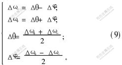
����-�ͦ���+�ɷֱ���ͼ4��ͼ5��ʾ��(113)��X��������ͼ�����Ƿ�ͳĵ��ľ�����,���Ⱥͦյ�����ֵ����ʽ(9)��õĦ��Ⱥͦ��մ���ʽ(8),�����([SX(]��a[]a[SX)])����([SX(]��a[]a[SX)])��,���ɽ�һ���õ�a����a����
��arΪ��ȫ��ԥ״̬Si1-xGexĤ�ľ�����,ar����a����a�����[19]:
![]()
����:![]() ,Ϊ���ɱ�;c11��c12��Ϊ������ģ��;��c11��c12��ֵ[5],����æ�=0.278��
,Ϊ���ɱ�;c11��c12��Ϊ������ģ��;��c11��c12��ֵ[5],����æ�=0.278��
Si1-xGexĤ��Ge+����x��ar��ϵΪ[19]:
![]()
ʽ(11)ͬʱ�����˴�ֱ��������ھ������ı仯,�������������ȷ��
2.2 �������ӵļ���
��Si1-xGex���ʽ���,����SiGeĤ��Ӧ���ԥ���Կ��ù�������f��ʾ,�䶨��Ϊ[20]:
![]()
��f=1,a��=aSi,Si1-xGexĤ���ھ�������ĵ�Si��������ͬʱ,��Ϊ��ȫ����;��f=0,a��=ar,Si1-xGexĤ���ھ���������ȫ��ԥ״̬��ͬʱ,��Ϊ��ȫ��ԥ��
3 �����������
������������,ѡ��ͼ2~5���д����Ե����߽��м���,�������õ����г���:
��=0.15405 nm; aSi=0.5431 nm; aGe=0.5658 nm[21]��
��2��ʾΪ����(004)��X��������ͼ�ļ�������
�� 2 (004)��X����������ļ�����
Table 2 Calculating results of X-ray diffraction patterns on plane (004)
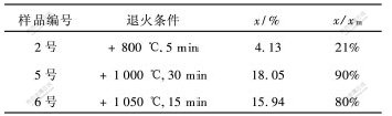
����ͼ2(b)~(e)��4�����ߵ����Ƿ�λ�ýӽ�,���x(Ge)���,���ֻ��ѡ�����е�1�����м��㼴�ɡ�����������:ֱ��1000 ��,5 min�˻��,��ע���Լ80%��Ge+��δ�������λ�á���ͼ3����(b),(c)���м���,�������:��1000 ��,30 min�˻��,Ge+������18.05%,��ע���90%��Ge+�Ѵ������λ�á���������˻��¶Ⱥ��ӳ��˻�ʱ��(+1050 ��,15 min),�˻�Ч����������[18]��
����(004)��X�������������������Ge+Ũ��x�������,������(113)����������,�����ɵõ���Ϊ��ȷ��xֵ,���ɵõ���������f,��Ҫ���㲽������:
a. ��(113)���������ʽ(4),�óĵ��λ�æ�,�����(113)��(001)��нǦյ�����ֵ;
b. ��ͼ4��ͼ5��æ���-�ͦ���+,����ʽ(9)�æ��Ⱥͦ���;
c. ��ʽ(8)����![]() ���
���![]() ,����ʽ(10)����ar��ֵ;
,����ʽ(10)����ar��ֵ;
d. ����ʽ(11)��ʽ(12)�ֱ��Ge+����x����������f��
��(113)���X�������������з���,���������3��ʾ��
�� 3 (113)��X������������ļ�����
Table 3 Calculating results of X-ray diffraction patterns on plane (113)
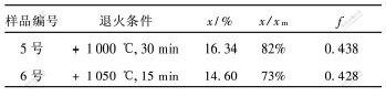
�ɼ�,�������ھ������ĸı��,�õ���Ge+�������н��͡�������������:����˻��¶�,�ӳ��˻�ʱ����ʹ��ռ�����λ�õ�Ge+������������,���Թ�������Ӱ�첻������UVCVD���Ʊ���Si1-xGex���ʽ����[20],fֵ�Ե�,���λ���ȱ���ܶȿ��ܽϴ�
��ͼ2~5���ɿ���,X��������ͼ��SiGe����ȽϿ�,ǿ�Ȳ�̫��,˵������Ge+ע���,����Si1-xGexĤ�Ľᾧ�����д����,��ͱ�ɢ��ķ��������һ�µ�[18]����һ�����������ΪGe+�����ϴ�,������ע��ʱ,�������ؾ�������,�侭��ʱ���˻�,���澧��Ļָ����Dz�̫����;��һ����,Ҳ��Ӧ���ԥ�������ͷŵĴ���λ����ȱ���йء�
4 �� ��
��SIMOX��Ʒ��ע�����Ge+,ע������Ϊ100 keV,ע�����Ϊ5.3��1016/cm2,Ȼ���ע����Ʒ���п������˻�ͨ����(004)��(113)��X�������������ߵķ�����֪,��1000 ��,30 min�˻��������˻�Ч���Ϻá��ڴ�������,��ע���82%��Ge+ռ�����λ��,��������Ϊ0.438�����ڸ���Ge+ע���������ؾ��������Լ�Ӧ���ԥ�����д�����λ����ȱ���ͷŵ�,����ᾧ������̫���롣
��л
����ʵ�鲿�ֵĹ����������ڰµ���Linz��ѧ�뵼���о��������ڼ���ɵġ��ڴ��ڼ�,��ʦLeopold Palmetshofer�����˰�����ָ��;Tanzer Claus��������ע��ʵ��,Heize Ellmer������RBS����;�й���ѧԺ�뵼���о������²�ʿׯ������X���� ���Բ������߽��������������̽��,�ڴ�һ����ʾ��л��
�����:
[1]֣��ֲ. �˹����Լ���[M]. ��ɳ:���ϿƼ�������,1997.
ZHENG Hou-zhi. Artificial cutting to properties of matter[M]. Changsha: Hunan Science and Technology Press, 1997.
[2]Ahaja R,Persson C, Ferreira A, et al. Optical properties of SiGe alloys[J]. J Appl Phys, 2003, 93(7):3832-3836.
[3]Mitchell M J, Ashburn P, Bonar J M, et al. Comparison of arsenic diffusion in Si1-xGex formed by epitaxy and Ge+ implantation[J]. J Appl Phys, 2003, 93(8):4526-4528.
[4]Konig U, Gruhle A. Advanced concepts in high speed semiconductor devices and circuits[A]. Proceeding of the 1997 IEEE/Cornell Conference[C]. Ithaca NY: IEEE, 1997.
[5]LU Xiang, Cheung N W. Synthesis of SiGe and SiGeC alloys formed by Ge and C implantation[J]. Appl Phys Lett, 1996, 69(13): 1915-1917.
[6]Temkin H, Bean J C, Antresyan A, et al. GexSi1-x strained layer heterostructure bipolar transistor[J]. Appl Phys Lett, 1988, 52(13):1089-1091.
[7]����,������. �¶ȡ�Ge�����Ͳ���Ũ�ȶ�Si1-xGex�������ȵ�Ӱ��[J]. �뵼��ѧ��, 2001, 22(9): 1122-1126.
JIN Hai-yan, ZHANG Li-chun. Bandgap narrowing of strained Si1-xGex as a function of Ge fraction, temperature and impurity concentration[J]. Chinese Journal of Semiconductor, 2001, 22(9): 1122-1126.
[8]�����. �����뵼����ϵı����ѧ����[M]. ����:������ѧ������,2002.
XU Zhen-jia. Surface science aspects of current semiconductor materials[M]. Beijing: Peking University Press, 2002.
[9]Yamada A, Tanda M, Kato F, et al. Gas source molecular beam epitaxy of Si and SiGe using Si2H6 and GeH4[J]. J Appl phys, 1991, 69(2): 1008-1012.
[10]Bean J C, Sheng T T, Feldman L C, et al. Pseudmorphic growth of GexSi1-x on silicon by molecular beam epitaxy[J]. Appl phys Lett, 1984, 44(1): 102-104.
[11]Meyerson B S. Low temperature silicon epitaxy by ultrahigh vacuum chemical vopor deposition[J]. Appl phys Lett, 1986, 48(12): 797-799.
[12]Songsiriritthigul P, Holmen G. Thermal solid phase epitaxial growth and ion beam induced crystallisation of Ge+ ion implanted layers in silicon[J]. Nuclear Instruments and Methods in Physics Research B, 1996,120: 207-211.
[13]Corni F, Frabboni S, Ottaviani G, et al. Solid phase epitaxial growth of GeSi alloys made by ion implantation[J]. J Appl Phys, 1992, 71(6): 2644-2649.
[14]Cristiano F, Nejim A, Mauduit DE B, et al. Characterization of extended defects in SiGe alloys formed by high dose Ge+ implantation into Si[J]. Nuclear Instruments and Methods in Physics Research B, 1996, 120: 156 -160.
[15]King A C, Gutierrez A F, Saavedra A F, et al. Defect evolution of low energy, amorphizing germanium implants in silicon[J]. J Appl Phys, 2003, 93(5):2449- 2452.
[16]������,�����,������,��. GexSi1-x/SiӦ��㳬����X-����˫��������˶�ѧ�о�[J].�뵼��ѧ��,1992,13(1): 14-21.
DUAN Xiao-feng, FENG Guo-guang, WANG Yu-tian, et al. Double crystal X-ray diffraction study of GexSi1-x/Si strained layer superlattices by kinematical approach[J]. Chinese Journal of Semiconductors, 1992, 13(1): 14-21.
[17]Ziegler J F. Handbook of ion implantation[R]. North-Holland: Elsevier Science Publishers, 1992.
[18]������,����,������. ���и���������ע��Ŀ������˻��о�[J].���ϵ���, 2004,18(7): 101-103.
LUO Yi-min, CHEN Zhen-hua HUANG Pei-yun. Research on rapid thermal annealing of high dose Ge+ implantation into silicon[J]. Materials Review, 2004, 18(7):101-103.
[19]Pearsall T P, Strained layer superlattices materials science and technology[M]. New York: Academic Press,1995.
[20]��,�����,�ɲ���,��. Annealing behavior of Si1-xGex/Si heterostructures[J]. �뵼��ѧ��,2000, 21(10): 962-965.
YU Zhuo, LI Dai-zong, CHENG Bu-wen, et al. Annealing behavior of Si1-xGex /Si heterostructure[J]. Chinese Journal of Semiconductor, 2000, 21(10): 962-965.
[21]������.�뵼������ѧ[M]. ����:��ѧ������,2000.
LI Ming-fu. Semiconductor physics[M].Beijing: Science Press, 2000.
�ո�����:2004-10-28
������Ŀ:���ϴ�ѧ��������������Ŀ(9809GZ05)
�����:������(1957-),��,���������,������,���°뵼������о�
������ϵ��: ������,��,������;�绰:0731-8877121(H);E-mail:Luoym1957@sina.com
[1]֣��ֲ. �˹����Լ���[M]. ��ɳ:���ϿƼ�������,1997.
[7]����,������. �¶ȡ�Ge�����Ͳ���Ũ�ȶ�Si1-xGex�������ȵ�Ӱ��[J]. �뵼��ѧ��, 2001, 22(9): 1122-1126.
[8]�����. �����뵼����ϵı����ѧ����[M]. ����:������ѧ������,2002.
[16]������,�����,������,��. GexSi1-x/SiӦ��㳬����X-����˫��������˶�ѧ�о�[J].�뵼��ѧ��,1992,13(1): 14-21.
[17]Ziegler J F. Handbook of ion implantation[R]. North-Holland: Elsevier Science Publishers, 1992.
[18]������,����,������. ���и���������ע��Ŀ������˻��о�[J].���ϵ���, 2004,18(7): 101-103.
