Fabrication of grating waveguide using photopolymerization
YAO Shu-shan(Ҧ��ɽ)1, QIN Xiao-yan(������)1, YU Xiao-qiang(����ǿ)1,
ZHANG Qi(�� ��)1, XU Guang-hu(�����)1, WANG Ze-yan(������)1,DONG Yi(�� ��)2,
JING Xiang-yang(������)1, SUN Yu-ming(������)2, HUANG Bai-biao(�ưر�)1
1. State Key Laboratory of Crystal Materials, Shandong University, Ji��nan 250100, China;
2. Department of Optics, Shandong University, Ji��nan 250100, China
Received 10 April 2006; accepted 25 April 2006
Abstract:
Two ternary materials systems, which comprise photoinitiator/two-photon initiators, oligomer and binder were prepared. Polymeric waveguide film was manufactured by spinning the materials on optical glass (refraction index=1.5), the two-photon initiated photopolymerization (TPIP) and single-photon holographic photopolymerization were carried out respectively in the polymer waveguide film. The preparation of these materials was explained and absorption spectra were tested. The experimental results including the micrographs and diffraction patterns verifying the formation of grating waveguide structures were given. The results show that grating waveguide microstructures can be holographically fabricated by single-photon photopolymerization with low-power (tens mW ) continuous-wave (CW) laser at 532 nm successfully. Because the continuous-wave laser at 532 nm is handier than one at 514 nm.
Key words:
two-photon initiated photopolymerization; grating waveguide;
1 Introduction
Integrated optical waveguides and devices have applications in optical sensors and communication systems. Polymers appear to be very suitable for integrated optics applications. They can be deposited directly on any kind of substrates, unlike other optical waveguide materials such as silica (SiO2), lithium niobate (LiNbO3), and III-V compound semiconductor materials. Their low cost and simple processing are much more alluring than SiO2-based materials. They can be processed as multilayer films on semiconductor substrates and patterned via photolithography and oxygen plasma etching in order to define waveguide layouts for integrated optics.
Polymeric waveguide gratings were regarded applicable to industry in the near future, since most of the critical disadvantages of polymeric waveguide gratings are recently overcome. The main problems of polymeric waveguide gratings were a relatively high waveguide loss and a relatively high temperature and polarization dependence.
Since the first waveguide grating was reported in 1970, the researchers have rapidly found its potential in integrated optics. Increasing demands for inexpensive, reliable and efficient waveguide grating lead many researchers to consider polymers [1]. Nowadays, the polymeric waveguide grating has been fabricated by means of various methods, such as holographic setups, e-beam direct writings, UV-photobleaching, laser ablation and photoisomerisation [2-6]. The diverse optical properties of polymeric waveguide grating, for instance, all optical switches, photonic band-gap and resonant grating-waveguide structure [7-9], have been characterized extensively.
So far, most methods to form a grating in polymeric waveguide are physical, while there is no chemical change in polymeric waveguide during the process. In other methods, the process of preparation is very complex. Recently, SUTHERAND et al [10] have fabricated a grating with electrically switchable properties by using TPIP. In this work, a fabrication method of coupling grating is presented by means of TPIP. Compared to those methods above, the TPIP technique possesses some particular advantages, such as convenience, flexibility, cheapness and automatization. Moreover, the microstructure feature of coupling grating, waveguide mode and transmission loss of the polymeric film are investigated, respectively.
In 2000, a microstructure was fabricated by using the holographic technique [11]. However, the 355 nm is too short to allow a deeper penetration. Most recently WANG et al [12] attempted the holographic preparation of microstructures using a continuous-wave (CW) laser at 514 nm.
Because the CW laser at 532 nm is handier than one at 514 nm, it will be beneficial to realize the holographic fabrication of grating waveguides structures by means of a CW laser at 532 nm. In this work, we report the successful use of a low-power ( tens mW) CW laser at 532 nm in making a grating waveguides by single-
photon holographic photopolymerization with our new synthesized photopolymer recording material including a special photoinitiator. We will first explain the preparation of this material and its property of spectral absorption, and then give the experimental results. The diffraction patterns of the resultant structure were also provided to verify the formation of grating waveguide.
2 Material preparation and optical system
2.1 Materials preparation
Two ternary materials systems, which comprise photoinitiator/two-photon initiators, oligomer and binder were prepared in this work.
2.1.1 Synthesis of initiator used for one-photon holographic
To realize the holographic fabrication at 532 nm, an appropriate photoinitiator must be synthesized first. The synthetic path is shown in Fig.1.

Fig.1 Synthesis path of holographic photoinitiator
1.7 g of eosin (0.002 46 mol) is refluxed and dissolved in 120 mL of dichloromethane. To this solution is added a transparent solution of the diaryliodonium hexafluoroantimonate (3.0 g, 0.006 78 mol) and dichlo-romethane (30 mL). After refluxed and stirred at room temperature for 12 h, the solvent is removed by distilling. Then the residue is extracted using absolute ether. After filtrating and washing the filter residue with absolute ether, we can remove the solvent. The final product can be obtained by drying in air.
To prepare the photopolymer for single-photon holographic fabrication, a 5 g urethane acrylate (Sarto-mer Co. Product No: CN 965) and 1 g poly (styrene-co-acrylonitrile) (AlDRICH Co.) are dissolved in 95 g of 1, 2-dichloroethane. The indissoluble impurity in the solution is then filtrated and 0.05 g of photoinitiator is added into the solution. After the 1, 2-dichloroethane is volatilized in air at room temperature, the resulting photopolymer can be used for holographic fabrication.
2.1.2 Liner absorption spectra of photopolymer
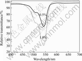
The liner absorption spectra of this photopolymer are tested and the results are shown in Fig.2. Here the solid line and the dashed one represent the absorption of the material with the photoinitiator consistencies 0.5% and 1%. From these curves we can clearly see the absorption peak at 532 nm. Consequently it can be used as a holographic recording material at this wavelength.

Fig.2 Absorption spectra of photopolymer
2.1.3 Synthesis of initiator used to TPIP
The synthesis and characterization a high effective initiator for TPIP were the key work of this paper. E-1,4-bis[4��-(N,N-di-n-butylamino)styryl]benzene Calcd for C38H52N2: C, 85.02; H, 9.76; N, 5.22. Found: C, 84.78; H, 9.92, N, 5.32.��was synthesized which is mentioned in Ref.[13] (as shown in Fig.3). 5 g PMMA(average M.W. 15000, GPC) was dissolved in 95 g 1,2-dichloroethane, a mixture of 2.5 g oligomer (urethane acrylate : Sartomer Product No. CN 965) and 0.01 g initiator was added to 10 mL of the solution.
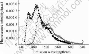
One-photon(400 nm) and two-photon(800 nm) fluo-
rescence spectra of initiator are shown in Fig.4. The liner absorption spectra of this photopolymer are not shown in this paper. We used a mode-locked Ti: sapphire laser

Fig.3 Initiator used to TPIP
(Coherent Mira 900 F) with 76 MHz and -200 fs pulse to test fluorescence spectra.

Fig.4 One- and two-photon Fluorescence spectra
2.2 Preparation of polymeric waveguide film
After ultrasonic shake, the indissoluble impurities in the solutions were filtrated respectively. The films were prepared by spin coating on optical glass with a refractive index of 1.5 under 1 800 r/min and soft-baking procedures, and the thickness of the films was between 1 ��m and 2��m.
2.3 Optical system for grating waveguide fabrication
Generally speaking, the interference of two noncoplanar plane waves can form an 1D periodic microstructure [14]. The optical system will not be mentioned in this paper. We have successfully fabricated a series of grating waveguide microstructures with our photopolymer and an 100 mW CW laser of 532 nm. The actual power for recording the volume holograms is only about 10 mW due to the loss of optical elements used in experiments.
For fabricating the coupling grating in this TPIP polymeric waveguide film, we used a mode-locked Ti: sapphire laser (Coherent Mira 900 F) with 76 MHz and -200 fs pulse and a computer-controlled stepper motor-driven XY stage.
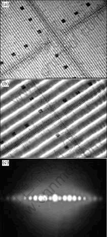
3 ResultsIn the following we provide some microscopic photos and diffraction patterns of the resultant structures. All the diffraction patterns are obtained with a 25 mW He-Ne laser of 633 nm.
Fig.5 shows the photos formed by two beams with intersection angle 10.5? and 2.2? respectively. Their fringe periods are 2.9 mm and 14 mm. Accordingly, Fig.5 (c) shows the diffraction pattern of the microstructure shown in Fig.5(a).
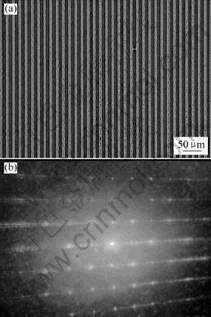
The average power of the laser was kept at 120 mW and radiation wavelength is 800 nm. The laser was focused using a microscope objective lens (100��). The

Fig.5 Experimental results of grating waveguide by one-photon holographic: (a) Photo of microstructure formed with angle 15?; (b) Photo of microstructure formed with angle 2.5?; (c) Diffraction pattern of (a)

Fig.6 Experimental results of TPIP: (a) Microscopic photo; (b) Interference pattern
periods of grating waveguide lines is 20 ��m and the scanning speed is 100 ��m/s. There are 400 exposed lines in the coupling grating. Concentration of initiator, objective lens, scanning speed of stage and energy of laser define the periods of grating waveguide. The least periods is 1.5 ��m under the present conditions of our lab.
4 ConclusionsA new photoinitiator especially for 532 nm was synthesized and then a photopolymer material for holographic recording was developed, and a series of experiments to test its usability in making grating waveguide with a low-power CW 532 nm laser. Compared to other methods with the use of high-power lasers, this technique is much more accessible to most laboratories and researchers. We believe it can have more practical applications.
TPIP will be more convenient to fabricate large scale applications. The microstructures by TPIP are generally fabricated by a time-consuming point-by-point scanning. Polymer gratings are fabricated based on photopolymerization. TPIP was demonstrated for the fabrication of coupling grating in a thin polymeric waveguide film. Our experiments verify the flexibility of microfabrication using TPIP. Moreover, the microstructure feature of the grating was investigated.
References[1] LEE J M, SUNTAK P, KIM M S, et al. Birefringence as a function of upper-cladding layers in polymeric arrayed waveguide gratings[J]. Opt Comm, 2004, 232: 139-144.
[2] MUKHERJEE N, EAPEN B J, KEICHER D M, LUONG S Q, MUKHERJEE A. Direct determination of the band-gap states in hydrogenated amorphous silicon using surface photovoltage spectroscopy[J]. Appl Phys Lett, 1995, 67: 371-373.
[3] OH M C, LEE M H, AHN J H, LEE H J, HAN S G. Polymeric wavelength filters with polymer gratings[J]. Appl Phys Lett, 1998, 72: 1559-1561.
[4] AHN S W, SHIN S Y. Post-fabrication tuning of a polymeric grating-assisted codirectional coupler filter by photobleaching[J]. Opt Commun, 2001, 194: 309-312.
[5] KLEIN J H, BADER M A, BAUEr I et al , Ablation dynamics of periodic nanostructures for polymer-based all-optical devices[J]. Synth Met, 2002, 127: 53-57.
[6] TOUSSAERE E, LABBE P. Linear and non-linear gratings in DR1 side chain polymers[J]. Opt Mater, 1999, 12: 357-362.
[7] BADER M A, KELLER H M, MAROWSKY G. Polymer-based waveguides and optical switching[J]. Opt Mat, 1998, 9: 334-341.
[8] BADER M A, MAROWSKY G. Bragg gratings in planar polydiactylene waveguides and their application in integrated optics[J].Synth Met, 2001, 124: 141-143.
[9] DONVAL A, TOUSSAERE E, ZYSS J, LEVY G, JONSSON E, FRIESEM A A. Novel polymer-based resonant grating-waveguide structures[J]. Synth Met, 2001, 124: 19-21.
[10] SUTHERLAND R L, TONDIGLIA V P, NATARAJAN L V, BUNNING T J. Switchable orthorhombic F photonic crystals formed by holographic polymerization-induced phase separation of liquid crystal[J]. Opt Express, 2002, 10: 1074-1082.
[11] CAMPBELL M, SHARP D N, HARRISON M T, DENNING R G, TURBERFIELD A J. Fabrication of photonic crystals for the visible spectrum by holographic lithography[J]. Nature, 2000, 404: 53-56.
[12] WANG X, XU J F, SU H M, et al. Three-dimensional photonic crystals fabricated by visible light holographic lithography[J]. Appl Phys Lett, 2003, 82: 2212-2214.
[13] BRIAN H, CUMPSTON, SUNDARAVEL P. Two-photon polymerization initiators for three-dimensional optical data storage and microfabrication[J]. Nature, 1999, 398: 51-54.
[14] CAI L Z, YANG X L, WANG Y R. Formation of a microfiber bundle by interference of three noncoplanar beams[J]. Opt Lett, 2001, 26: 1858-1860.
Foundation item: Project (2004CB719803) supported by the National Basic Research Program; Project(60377041) supported by the National Natural Science Foundation of China
Corresponding author: HUANG Bai-biao; Tel:+86-531-88364449; E-mail: bbhuang@sdu.edu.cn


