
���ι����������������ṹ�ݱ�
��ϲ��1, 2, ��С��3, ������4, �ı���1, ������1
(1. ������ѧ ������ѧ�빤�̼���ѧԺ, ���� 530004; 2. ���Ͻ�ͨ��ѧ ���Ͽ�ѧ�빤��ѧԺ, �ɶ� 610031;
3. �й���ѧԺ��ѧ�� ��������ѧ����ʵ����, ���� 100080; 4. �����ѧ ���Ͽ�ѧ�빤��ѧԺ, ���� 300044)
ժ Ҫ��
������羵�����������������ṹ���������ṹ��֯�ݱ������������о��� �������, �������Ʊ��κ�, ������ƽ�������ߴ�Ϊ50~70mm, ������λ���ṹ, ��û�з���λ���ѻ�����; �ھ��紦��������̨����ṹ, �Լ���̨����״���Ӧ��Ӧ�����Ķȡ� �ڱ��κ���, ���Կ����緢�䲻ȫλ���Ӷ���ʹ�������, ����������ߴ糤��(���������λ��)���˶����С� ��������ߴ糤��ʱ, ��ǰ�ؾֲ�����Ӧ�����, ֱ����Ӧ����һ��ֵʱ, λ��ֹͣ�˶�, ����ߴ�Ҳ���ٳ���, ��������̨�ṹ��
�ؼ���: ������; �۽ṹ; ���Ա���; ���; λ�� ��ͼ�����: TG0403
���ױ�ʶ��: A
Microstructure evolution of nanocrystalline nickel after cold-rolled deformation
ZHANG Xi-yan1, 2, WU Xiao-lei, ZUO Ru-lin3, XIA Bao-yu1, ZHOU Ming-zhe1
(1. School of Physical Science and Engineering Technology,Guangxi University, Nanning 530004, China;
2. School of Materials Science & Engineering,Southwest Jiaotong University, Chengdu 610031, China;
3. State Key Laboratory of Nonlinear Mechanics Institute of Mechanics,Chinese Academy of Sciences, Beijing 100080, China;
4. School of Materials Science and Engineering, Chongqing University, Chongqing 300044, China)
Abstract: The microstructures characteristics of the cold-rolled deformed nanocrystalline Nickel metal were studied by transmission electron microscopy (TEM).The results show that, after cold-rolled deformation, the average grain size is about 50-70nm. Few of dislocations are found in the deformed microstructure. There are step structures in the grain boundary (GB) and neighborhood area, and the contrast of stress field ahead of the step corresponds to the step in the shape. In the late stage of the deformation, with the grain size growing up, the grain boundary can emit partial dislocations. The partial dislocations promote the creation of stack faults, and the size of the stack faults grows up with the gliding of the partial dislocation, so, it is easy to realize the deformation. When the size of stack dislocations grows up, the local deformation stress ahead of the step gradually become big. When this stress reaches a critical value, the gliding of the partial dislocations stops, the stack faults will stop growing up and leave the step structure behind.
Key words: nanocrystalline; microstructure; deformation; stack fault; dislocation
Ŀǰ, ����������ı��λ����в������ ��ƽ�������ߴ�С��100nmʱ, ����λ����Ӧ���ӽ����ۼ�Ӧ���� ����������������, ����λ����Ӧ���ӽ����ۼ�Ӧ���ľ����ٽ�ߴ��СΪ20~40nm[1], ���, �ڳ�ϸ���������ʱλ���Ƿ��γɲ��ѻ�, �Լ�λ���Ƿ������Ա��λ������[2]�� �ڽ�����������о���, �������������ṹ����������Al[3], Ni[4], Cu[5]�����������ṹCo[6]�д����Ͼ��Ͳ��ȱ��, ��Cu�������д��ھ��绬��[7, 8]�� Kumar��[9]ͨ������������۲��������ʱ, �����ڽ�������������, λ�������Ա���������Ҫ����, λ�����緢��;��ڻ����Լ���Э������֮��Ļ������ٽ����紦�����澧�羧��֮���϶���γɡ� ��Hugo��[10]��Ϊ, ������羵ԭλ������Ʒ̫��, ���۲쵽��λ��������Դ������λ��Դ, �������ȱ��, ����в���֤��λ���ڱ���������Ҫ���á� Budrovic��[11]�о��˵�����������ι����е�X��������, �����ڱ��κ�ж��ʱ, ���������ǿ����, �Ӷ�Ԥʾ���ι��̲�δ��ɲ���λ���ѻ��Լ��ӹ�Ӳ�����̡�
Ϊ��������������ı��λ���, �ѽ�����һЩ����ģ�͡� Gutkin ��[12, 13]��Ϊ����������ı��λ��������ھ��绬�ƺ�Ťת���εĹ�ͬ���á� ���о���ģ����, ���ƾ���λ�������澧��ֽ�������ھ������Ƶ�λ��, ��������ظ��Ľ��е��¾���λ��ǽ������, �����������������о���������ת����Ťת���Ρ� Yamakov��[14]֤���������ߴ�С��һ��ֵʱ, ���в���λ���ܹ��ھ������γ�, ��Щλ���ܻ���ͨ�����������������Ѷ���, ֱ�����Dz�����澧��, ���Ѷ�������Ϊ��ȱ�ݱ����ھ����С� �������ڲ���һ�������ĶѶ�������ʱ, �Ͳ��ᷢ�������λ����ֳ�� ���, ������״̬�¾����ܴٽ�����, Ҳ������Ϊ���쵽����������λ������Դ�ͽ�����, ʹ��������һ���Ѷ���[15-18]�� ��������Al�ķ��Ӷ���ѧģ����չ����λ��-λ����λ��-�Ͼ���Ӧ, �Ӷ����¸��ӵ��Ͼ�����, �Լ��Ͼ����ͨ����״λ�����ӽṹ���γ�[14, 19]�� Ȼ��, �ڸ����о���, ����100nm���µ���ĥCu-Zr������ȴû�з���λ������[20], �����DZ�Ĥ��Ʒ�ʹ����Ʒ֮��ļ��γߴ���[21, 22], ����[9, 10]�еĽ����û��ȷ��֤������ȡ���ھ��緢��λ��; ��һ����, ֱ��ĿǰΪֹ��û�о��緢�������λ����ֱ��ʵ��֤�ݡ� ����й�����������ı��λ����д���һ���о���
��������������羵���������κ�����ṹ���������ṹ��֯�ݱ������������о�, ����ʵ�������������ۡ�
1 ʵ��
������������Ϊ�������Ʒ, ����������Ĵ���Ϊ99.8%, ���Ϊ0.25 mm�� ƽ�������ߴ�Ϊ20nm�� �������ṹ�˻�״̬�µ�SEM����ͼ1��ʾ�� ����������Ʒ�ߴ�Ϊ12.5mm��12.5mm�� ��Ʒ������������Ϊ35%��ȵ�ѹ������ ���е���Ʒ������Riguta D/max-RC X���������ǽ��з���(Cu ��, 40kV, 200mA; ɨ��, 20.0/70.0/0.2/0.2s). ��羵��Ʒ����˫�繤�ս������ռ�������, ��羵ΪPhilips Tecnai-2000, ���ٵ�ѹΪ200kV��
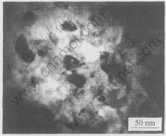
ͼ1 �˻����ṹ�������ľ����۽ṹ
Fig.1 Microstructure of grain of nanocrystalline Nickel annealed
2 ��������
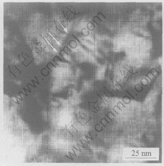
��羵�۲����, �������Ʊ��κ�, �������ľ�����״��δ�����ܴ�ı�, �������ߴ�ȴ�����˽ϴ�仯, �������Ʊ��κ�, ������ƽ�������ߴ�Ϊ50~70nm(��ͼ2)�� ��ͼ2�ɿ���, ���־�����������Կ������ƳĶ�, �������۲����ת����, ����Ī�������� ͬʱ, ���ھ����ߴ�̫С, ʵ�����ڱ����������ྦྷ����ص�, ����ڵ羵�µ������������п��ܲ��ǵ����� ���������ܳĸ���ЧӦ, ������Ī����������(��ͼ3)�� �ڸ�������ȴ�ܷ�����λ���ṹ, �������, ������������������֮��ľ��紦��̨����ṹ(��ͼ4)�� ͼ4�е�̨��ǰ����������̨����״���Ӧ�ijĶ�����Ϊ����Ӧ�����Ķ�(���ͷ��ʾ)�� ͼ5��ʾΪ��һ�ӳ����������侧�紦̨�ס�
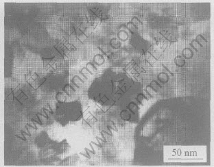
ͼ2 ���ṹ����������۽ṹ
Fig.2 Microstructure of nanocrystalline Nickel after cold-rolled
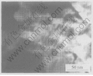
ͼ3 �������ṹ������Ī�����Ƶ�TEM��
Fig.3 TEM image of morie strips for cold rolled nanocrystalline Nickel
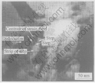
ͼ4 ���ṹ����������̨�ṹ������֯
Fig.4 Microstructure of step for cold-rolled nanocrystalline Nickel
��ͼ4��5�ɿ���, �ڱ��κ���, ���ھ����ߴ�����, λ���ܹ��ھ������γ�, ��ά�ֱ��ι��̽���[12-14], ���������״̬�¾����ܴٽ����Ƶ�����[15-18], �ƺ������þ��緢�䲻ȫλ���ٷ��������ʵ�������������ĺ��ڱ��ι��̡� Muller��Solenthaler[23]����ϸ�����˶ྦྷ���ϵ�λ��-�Ͼ��������õ����⡣ һϵ��Ф������ȫλ�����Ͼ��練Ӧ, �ɽ�����һ��ԭ�Ӳ�ķ��Ͼ��������Ͼ�����ʧ�����Ͼ��ĶϿ�, ������̲�����ԭ�����ھ��緢��λ���� ���ṹ�������������ļ����ģ����ʾ[14], �ھ�����Գ�Ϊλ��Դ�ı���������, �ɾ������ɵ�һϵ�в�ȫλ��, ���������Ͼ���������֮ǰ���˶��н�����һЩ����ṹ�ۼ�, ���Ͼ��������õĽ����ʹ�Ͼ����ȳߴ��խ, �����γ���ν�Ľ����Ͼ�, ������������ߴ�(70~100nm)�Ľ����������Գ��ָ����Ͼ�����ṹ�� ��ͼ4���ɿ���, �Ӷ���ʹ���緢��λ�������ɲ��, ������������ͼ�е�̨�ṹ�� Ȼ��, �þ����в�û���Ͼ�, ȴ��̨��ǰ���������Ӧ�����Ķ�, ˵���ڱ��о�, �Ͼ���λ��(����)�Ľ�������[12, 13, 14, 23] ������ά�ֱ��ι��̵ı�Ҫ������ ���Һ��п���, ����Ʒ���εĺ���, �������ߴ糤�ӽ�100nmʱ, ���ν������緢�䲻ȫλ���Ӷ��ٷ����ɲ��, �������ڲ����ߴ�ij���, �༴��������λ�����˶��͵��Խ��С� ��������ߴ糤��ʱ, ��ǰ�ؾֲ�����Ӧ�����, ֱ����Ӧ����һ��ֵʱ, λ��ֹͣ�˶�, ����ߴ�Ҳ���ٳ���, �Ӷ�������̨�ṹ(��ͼ6)�� ���ھ���λ���Ƿ���������澧��ֽ�������ھ�
ͼ5 ��һ�ӳ��е�̨��
Fig.5 Microstructure of step in another area
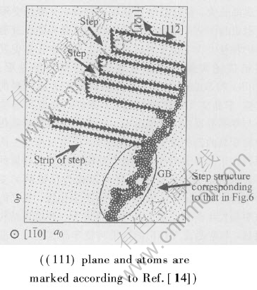
ͼ6 (111)���治ȫλ���ھ��紦�γɵIJ���Ͳ�ȫλ�����ƵIJ���˶�
Fig.6 Stack faults formed by partial dislocations gliding on grain boundaries of (111) crystal plane and movement of partial dislocations gliding corresponding to Figs.5 and 6
�����Ƶ�λ��[12, 13], �Ӷ����¾���λ��ǽ������, �������������������о���������ת���ݱ��λ����һ��ʵ��۲졣
3 ����
�������Ʊ��κ�, ������ƽ�������ߴ�Ϊ50~70mm, ����������λ���ṹ, ��û�з���λ���ѻ����ᡣ �ھ��紦��������̨����ṹ, �Լ���̨����״���Ӧ��Ӧ�����Ķ�, ��ʾ�ڱ��κ���, ���ο��Կ����緢�䲻ȫλ���Ӷ���ʹ����ķ���, �������ڲ���ߴ�ij���, �༴�������λ���˶��Ľ��С� ��������ߴ糤��ʱ, ��ǰ�ؾֲ�����Ӧ�����, ֱ����Ӧ����һ��ֵʱ, λ��ֹͣ�˶�, ����ߴ�Ҳ���ٳ���, �Ӷ�������̨�ṹ��
REFERENCES
[1]Legros M, Elliott B R, Rittner M N, et al. Microsample tensile testing of nanocrystalline metals[J]. Phillos Mag A, 2000, A80: 1017-1026.
[2]van Swygenhoven H, Weertman J R. Preface to the viewpoint set on: mechanical properties of fully dense nanocrystalline metals[J]. Scripta Materialia, 2003, 49: 625-627.
[3]Chen M, Ma E, Hemker K J, et al. Deformation twinning in nanocrystalline aluminum[J]. Science, 2003, 300: 1275-1277.
[4]Kumar K S, Suresh S, Chisholm M F, et al. Defor-mation of electrodeposited nanocrystalline nickel[J]. Acta Mater, 2003, 51: 387-405.
[5]Wang Y, Chen M, Zhou F, et al. High tensile ductility in a nanostructured metal[J]. Nature, 2002, 419: 912-914.
[6]Sort J, Zhilyaev A, Zielinska M, et al. Microstructural effects and large microhardness in cobalt processed by high pressure torsion consolidation of ball milled powders[J]. Acta Mater, 2003, 51: 6385-6393.
[7]Lu L, Sui M L, Lu K. Superplastic extensibility of nanocrystalline copper at room temperature[J]. Science, 2000, 287: 1463-1466.
[8]Cai B, Kong Q P, Cui P, et al. Creep behavior of cold-rolled nanocrystalline pure copper[J]. Scripta Mater, 2001, 45: 1407-1413.
[9]Kumar K S, Suresh S, Chisholm M F, et al. Defor-mation of electrodeposited nanocrystalline nickel[J]. Acta Mater, 2003, 51: 387-405.
[10]Hugo R C, Kung H, Weertman J R, et al. In-situ TEM tensile testing of DC magnetron sputtered and pulsed laser deposited Ni thin films[J]. Acta Mater, 2003, 51: 1937-1943.
[11]Budrovic Z, van Swygenhoven H, Derlet P M, et al. Plastic deformation with reversible peak broadening in nanocrystalline nickel[J]. Science, 2004, 304: 273-276.
[12]Gutkin M Y, Ovid��ko I A, Skiba N V. Crossover from grain boundary sliding to rotational deformation in nanocrystalline materials[J]. Acta Mater, 2003, 51: 4059-4071.
[13]Fedorov A A, Gutkin M Y, Ovid��ko I A. Transformations of grain boundary dislocation pile-ups in nano- and polycrystalline materials[J]. Acta Mater, 2003, 51: 887-898.
[14]Yamakov V, Wolf D, Phillopt S R, et al. Dislocation-dislocation and dislocation-twin reactions in nanocrystalline Al by molecular dynamics simulation[J]. Acta Mater, 2003, 51: 4135-4147.
[15]van Swygenhoven H. Polycrystalline materials[J]. Science, 2002, 296: 66-67.
[16]Schi��tz J, Jacobsen K W. A maximum in the strength of nanocrystalline copper[J]. Science, 2003, 301: 1357-1359.
[17]van Swygenhoven H, Derlet P M, Hasnaoui A. Atomic mechanism for dislocation emission from nanosized grain boundaries[J]. Phys Rev B, 2002, B66: 024101.
[18]Derlet P M, Hasnaoui A, van Swygenhoven H. Atomistic simulations as guidance to experiments[J]. Scripta Mater, 2003, 49: 629-635.
[19]Froeth A, van Swygenhoven H, Derle P M. The influence of twins on the mechanical properties of nc-Al[J]. Acta Mater, 2004, 52: 2259-2268.
[20]Morris D G, Morris M A. Microstructure and strength of nanocrystalline copper alloy prepared by mechanical alloying[J]. Acta Mter, 1991, 39: 1763-1767.
[21]Derlet P M, van Swygenhoven H. Fracture of nanolamellar materials: continuum and atomistic models with application to titanium aluminides[J]. Phillos Mag A, 2002, 82(12): 2397-2417.
[22]Farkas D, van Swygenhoven H, Derle P M. Intergra-nular fracture in nanocrystalline metals[J]. Phys Rev B, 2002, B66: 060101.
[23]Mullner P, Solenthaler C. On the effect of defor-mation twinning on defect densities[J]. Mat Sci Eng A, 1997, 230: 107-115.
������Ŀ: ������Ȼ��ѧ����������Ŀ(50471086, 50461001)
�ո�����: 2005-03-22; ������: 2005-08-08
�����: ��ϲ��(1958-), ��, ����, ��ʿ
ͨѶ����: ��ϲ��, ����; �绰: 0771-3234232; E-mail: kehen888@163.com
