
Trans. Nonferrous Met. Soc. China 27(2017) 722-732
Mechanism of Ag3Sn grain growth in Ag/Sn transient liquid phase soldering
Hua-kai SHAO1,2,3, Ai-ping WU1,2,3, Yu-dian BAO1,2,3, Yue ZHAO1,3, Gui-sheng ZOU1,3
1. Department of Mechanical Engineering, Tsinghua University, Beijing 100084, China;
2. State Key Laboratory of Tribology, Tsinghua University, Beijing 100084, China;
3. Key Laboratory for Advanced Materials Processing Technology, Ministry of Education, Tsinghua University, Beijing 100084, China
Received 6 January 2016; accepted 26 April 2016
Abstract:
Transient liquid phase (TLP) bonding is a potential high-temperature (HT) electron packaging technology that is used in the interconnection of wide band-gap semiconductors. This study focused on the mechanism of intermetallic compounds (IMCs) evolution in Ag/Sn TLP soldering at different temperatures. Experimental results indicated that morphologies of Ag3Sn grains mainly were scallop-type, and some other shapes such as prism, needle, hollow column, sheet and wire of Ag3Sn grains were also observed, which was resulted from their anisotropic growths. However, the scallop-type Ag3Sn layer turned into more planar with prolonging soldering time, due to grain coarsening and anisotropic mass flow of Ag atoms from substrate. Furthermore, a great amount of nano-Ag3Sn particles were found on the surfaces of Ag3Sn grains, which were formed in Ag-rich areas of the molten Sn and adsorbed by the Ag3Sn grains during solidification process. Growth kinetics of the Ag3Sn IMCs in TLP soldering followed a parabolic relationship with soldering time, and the growth rate constants of 250, 280 and 320 ��C were calculated as 5.83��10-15 m2/s, 7.83��10-15 m2/s and 2.83��10-14 m2/s, respectively. Accordingly, the activation energy of the reaction was estimated about 58.89 kJ/mol.
Key words:
transient liquid phase soldering; Ag3Sn; morphologies of grains; growth kinetics; activation energy;
1 Introduction
Wide band-gap semiconductors, including silicon carbide (SiC) and gallium nitride (GaN), are commonly considered as promising electronic materials that are used in high-temperature (HT) applications, such as aerospace, automotive, deep-well drilling and energy production industry [1-3]. This is attributed to their high operation temperature, for example, SiC power devices have been demonstrated to work at 600 ��C [3]. However, lack of qualified HT packaging technologies limits the development and market growth of the wide band-gap semiconductors. In recent years, transient liquid phase (TLP) bonding has been concerned and proven to be a superior candidate, since TLP-bonded joints fully consist of intermetallic compounds (IMCs) and have excellent thermal reliability. For example, �� phase (Ag3Sn) in Ag-Sn binary system can withstand operation temperature approximately 480 ��C according to the phase diagram. Nevertheless, growth process of the IMCs probably affects the mechanical integrity of the TLP-bonded joint, for example, voids were observed between Ag3Sn grain boundaries during Ag/Sn/Ag TLP bonding [4]. Furthermore, the large IMCs are very brittle [5], which may lead to serious problems under stressed conditions in operation. As a matter of fact, both of them depend on the morphology of the IMCs grains to some extent. Therefore, it is quite deserved to research mechanism of the IMCs growth in TLP bonding.
Evolution and morphologies of the IMCs between Sn-based solder and Cu, Ag and Ni substrates during conventional soldering have been extensively studied for many years [6-16]. It is reported that many factors affect the growth of the IMCs. Reactions apparently differ with each other under different soldering temperatures, especially for solid- and liquid-state conditions [6]. The Sn-based solders with different compositions also affect the morphologies of the IMCs [7]. Additions of nano- particles such as nano-TiO2 [8], nano-Al2O3 [9] and nano-ZrO2 [10], or other elements like Cr [11], Ni [12] and RE [13] to prepare composite solders are investigated popularly, and different growth processes of the IMCs are obtained. In addition, effects of the other factors like cooling rate [14], soldering time [15] and crystal orientation [16] on morphologies of the IMCs are also reported.
In this work, silver is chosen for the substrate due to its superior physical properties of ductility, high electrical and thermal conductivity, as well as excellent oxidation resistance [17]. However, there are few reports on the morphologies and growth kinetics of Ag3Sn grains between Sn-based solders and silver substrate [18-20], especially for the pure Sn with plating Ag during TLP soldering. Moreover, it was found that preparation of the substrate had a significant effect on the growth kinetics of the IMCs [21]. Therefore, understanding more about TLP reaction for the electroplated Ag with pure Sn is very important. In the present work, the major objective is concerned about the morphologies and growth kinetics of the IMCs formed in Ag/Sn TLP soldering. Based on soldering temperatures ranging from 250 ��C to 320 ��C for different time, growth mechanism of the Ag3Sn grains and adsorption process of the nano-Ag3Sn particles were deeply discussed.
2 Experimental
2.1 Preparation of samples
Polished pure Cu (99.9%) rod with dimensions of d10 mm �� 5.5 mm was successively electroplated with 2 ��m-thick Ni layer as barrier layer and 35 ��m-thick Ag layer as substrate, followed by washing in 5% nitric acid with an ultrasonic bath for 5 min, and then rinsed with deionized water and anhydrous alcohol. Meanwhile, commercial pure Sn foil (99.9%) with thickness of 50 ��m was used as interlayer, and cut to wafer with diameter of 10 mm, and subsequently cleaned in acetone and anhydrous alcohol. After that, Sn foil was placed on the surface of plating Ag layer, and isothermally heated in a vacuum furnace with vacuum degree of lower than 2��10-3Pa. Soldering process was conducted at temperatures of 250, 280 and 320 ��C for various time ranging from 30 to 300 min, and the soldered samples were naturally cooled to room temperature.
The samples used to observe morphologies of the IMCs on top-view were deeply etched for 2-3 h by a solution of 93% CH3OH, 5% HNO3 and 2% HCl (volume fraction) to resolve away the residual Sn. Other TLP joints were mounted and polished to study evolution process of the IMCs. In addition, morphology analysis was carried out using a scanning electron microscope (SEM), and energy dispersive spectroscopy (EDS) was also utilized to identify compositions of the marked zones.
2.2 Measurement of Ag3Sn grain size
In order to improve the accuracy, two methods were adopted to measure the radius of Ag3Sn grains. The first way was classical linear intercept method referred to GB 6394-2002, and grain size was calculated by the following expression:
 (1)
(1)
where  is the average radius of Ag3Sn grains for one condition,
  is the average intercept, L0 is the length of the calculated line, N is the number of the knots, sp is the plotting scale of the SEM image.
Another way was statistic method introduced in the following. Firstly, the top-view SEM image of the IMCs for one condition was processed to extract grain boundaries with a special software, as shown in Fig. 1. Secondly, Image Pro Plus 6.0 was utilized to calculate the radius of every Ag3 Sn grain. Thirdly, frequencies of the values of grain size in different ranges were satisficed and fitted by Gauss function:
 (2)
(2)
where RC is the calculated radius of the Ag3Sn grains. According to Eq. (2), grain size for Ag3Sn could be obtained. Several SEM images for one condition were processed and used to calculate corresponding grain radius, and these values were averaged as the final result.
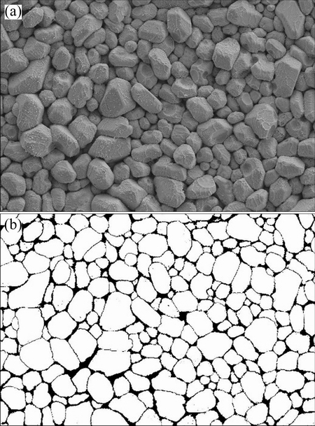
Fig. 1 Images before (a) and after (b) extraction for Ag3Sn grain boundaries
3 Results
3.1 Cross-sections of Ag/Sn TLP joints
Interfacial microstructures of the Ag/Sn TLP joints soldered at 280 ��C for different time were evaluated using SEM, and the residual Sn was mildly etched for about 30 s with corrosion solution before examination. As shown in Fig. 2, scallop-type Ag3Sn grains were observed on the substrate after soldering for 30 min (Fig. 2(a)), and groove-like structure was made up by two neighboring grains, which was so-called molten channel for the diffusion of Ag atoms from substrate [19,22]. In the study of ripening process of scalloped Cu6Sn5, KIM and TU [23] proposed that the selective reaction of Cu with Sn and expelling of the nonreactive Pb, Bi or Ag into the molten solders resulted in formation of the scalloped shape of the IMCs. However, in our work, we considered that grain boundary grooving and anisotropic mass flow were the dominant mechanism for that according to Ghosh��s study [24]. Thickness of the Ag3Sn layer increased with prolonging soldering time, while the number of grains in unit area reduced due to grain coarsening. The scalloped morphology was still stayed with continuing reaction, but curvature of the Ag3Sn grains gradually decreased, especially for that of 90 min (Fig. 2(c)) and 150 min (Fig. 2(d)). This revealed that Ag3Sn scallops would turn into more planar with soldering time, which may be attributed to grain coarsening and anisotropic mass flow of the Ag atoms.
3.2 Morphologies of Ag3Sn grains
Figure 3 showed top-view SEM images of the Ag3Sn grains formed on plating Ag surface after reaction with Sn at 250 ��C. It could be clearly seen that the morphology of Ag3Sn grains mainly was scalloped, which was similar to the Cu6Sn5 scallops formed on polycrystalline Cu surface that reacted with molten Sn-Ag-Cu solder [18]. Grain size increased with the increasing soldering time, and differed with each other though under one condition, which related to different growth velocities of the IMCs grains in different areas. In addition, abundant nano-particles were observed on the surface of the Ag3Sn scallops for 30 min (Fig. 3(a)) and 150 min (Fig. 3(d)), this phenomenon also occurred in Sn-Ag/Cu or Sn-Ag-Cu/Cu system soldering [25-27], all of them had similar shapes and scales but the latter was formed on the Cu-Sn IMCs.
Figure 4 illustrated morphologies of the Ag3Sn grains formed on the substrate after reaction with Sn at 280 ��C for various time. Two different shapes of the Ag3Sn grains, including scallops for 30 min, 60 min and 150 min and few prisms for 90 min, were clearly observed. Interestingly, it was found that grain size of the prism-type Ag3Sn was commonly larger than that of the scallop-type under the same condition, and the former existed lonely on the primary scallops, as shown in Fig. 4(c). Furthermore, amount of nano-particles were also captured by the Ag3Sn grains after soldering for 30 min (Fig. 4(a)).
Figure 5 showed morphologies of the Ag3Sn grains formed on plating Ag surface after reaction with Sn at 320 ��C for different time. It was observed that several types of Ag3Sn grains existed and lots of nano-particles also appeared on the surface of the IMCs. After soldering for 30 min (Fig. 5(a)) and 90 min (Fig. 5(c)), irregular prism was the main shape of the Ag3Sn grains, and this kind of crystals had a remarkable feature of one backbone and two sharp corner. Furthermore, the space between two prism-type Ag3Sn grains was thicker than that of the scallop-type somewhat. It seemed that the number of the prism-type Ag3Sn grains appeared at 320 ��C increased in comparison to that at 280 ��C, which demonstrated that it was inclined to form prism-type IMCs under higher-temperature conditions. However, only scallop-type Ag3Sn grains were found for 60 min (Fig. 5(b)), and surface of the Ag3Sn grain became more discontinuous compared with the previous scallops. When the soldering time prolonged to 150 min, as shown in Fig. 5(d), some large hollow column-type Ag3Sn crystals were formed and distributed at the grain boundaries of the scallops, whose axial direction had an angle of <90�� with the surface of the substrate. LI et al [28] suggested that long Ag3Sn column formed with a screw dislocation mechanism first, and then, the core of the column dissolved into molten Sn due to its higher energy, which led to formation of the hollow column- type grain.
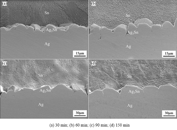
Fig. 2 Interfacial microstructures of Ag/Sn joints soldered at 280 ��C for different time
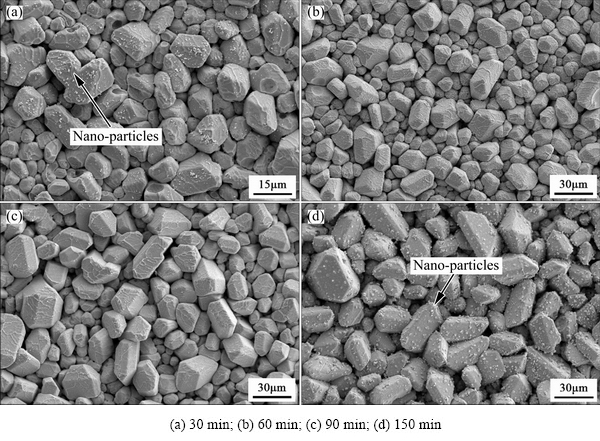
Fig. 3 Morphologies of Ag3Sn grains formed at 250 ��C for different time
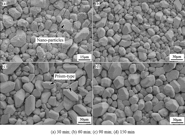
Fig. 4 Morphologies of Ag3Sn grains formed at 280 ��C for different time
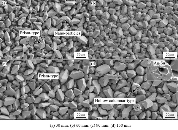
Fig. 5 Morphologies of Ag3Sn grains formed at 320 ��C for different time
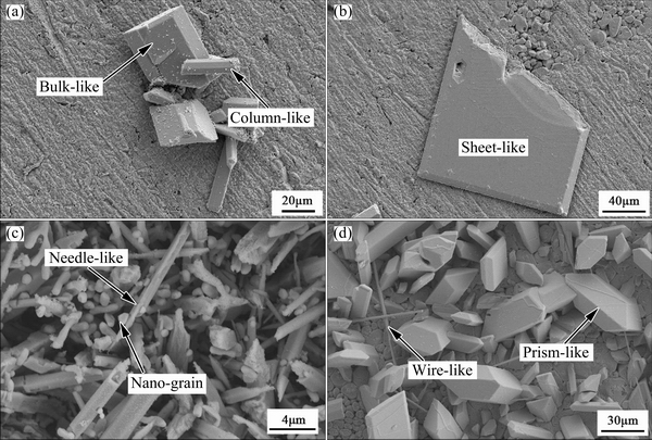
Fig. 6 Non-scallop-like shapes of Ag3Sn grains soldered at 250 ��C for 30 min (a), 250 ��C for 90 min (b), 280 ��C for 90 min (c) and 280 ��C for 300 min (d)
In addition, some other types of the Ag3Sn grains were also observed in Ag/Sn TLP soldering. After soldering at 250 ��C for 30 min (Fig. 6(a)), several large bulk- and column-like Ag3Sn crystals, as identified with EDS, formed on the primary IMCs that had planar and compact surface. As shown in Fig. 6(b), a large Ag3Sn crystal with sheet-shaped feature was found on the surface of the primary IMCs, whose morphology was similar to the above. Lots of slender Ag3Sn grains were observed on the substrate, as shown in Fig. 6(c), and they did not present prominent grain orientations. Meanwhile, many submicron particles were also formed and captured by these Ag3Sn needles. Besides, a few wire- and prism-like Ag3Sn grains appeared on the primary IMCs for the sample soldered at 280 ��C for 300 min.
Abnormal Ag3Sn grain was also found in the cross-sectional microstructure of the Ag/Sn TLP joint (Fig. 7(a)), and it could be seen that a crystal like butterfly was situated on the primary IMCs but not in the grain boundary. It was proposed that basic condition for the formation of the non-scalloped Ag3 Sn grain was that the primary IMCs had turned into planar morphology. Moreover, it was dominantly ascribed to anisotropic growth that Ag3Sn grains presented different shapes. However, how did the primary IMCs plane form? Just a new type of morphology? Or the IMCs evolution for a long time? This answer was found out according to cross-section of the TLP joint soldered at 250 ��C for 30 min. As shown in Fig. 7(b), many planar Ag3Sn grains were observed and made up a large plane, whereas, scalloped grains still existed at the same time. Therefore, it could be deduced that planar Ag3Sn grain represented a new morphology that was formed in a short soldering time.
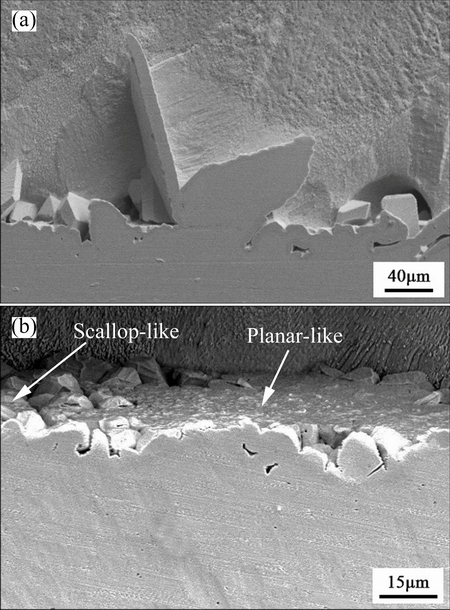
Fig. 7 Cross-sectional microstructures of Ag/Sn joints soldered at 250 ��C for 90 min (a) and 280 ��C for 90 min (b)
3.3 Growth kinetics of IMCs
Grain growth model was developed in Ref. [29], which was found to obey a power-law type t1/n kinetics. Especially, Ag3Sn grain growth was modeled as a diffusion driven process that could be expressed by
 (3)
(3)
 (4)
(4)
where R(t) is the average radius of the Ag3Sn grains under one condition, R0 is the initial radius when t=0, Kgb is the growth rate constant, Dgb is the grain boundary diffusivity, �� is the grain boundary energy, Vm is the molar volume of Ag3Sn, ��gb is the thickness of the grain boundary, R is the mole gas constant, T is the thermodynamic temperature. However, R0 was zero since reaction did not take place at the beginning, and Eq. (3) was simplified as following:
 (5)
(5)
This equation was very common to investigate the growth kinetics of the IMCs in conventional soldering, and mean grain size was generally plotted against the square root of the aging time [16,18].
Radius of Ag3Sn grains for the samples soldered at 250, 280 and 320 ��C for 30, 60, 90 and 150 min, were respectively calculated with linear intercept and statistic methods. As shown in Table 1, the values of grain radius increased with both increasing soldering time and temperature. In addition, it could be seen that the value measured with linear intercept method was slightly larger than that of the statistic method, which was resulted from the ignorance of the space between two grains for the former.
Table 1 Measured radius of Ag3Sn grains with linear intercept and statistic method
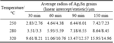
Figure 8(a) showed the IMCs growth changing with soldering time. It was found that measurements with two methods were successfully fitted by Eq. (5), and growth of Ag3Sn grains followed a parabolic law with soldering time. Furthermore, growth rate constants for 250, 280 and 320 ��C were calculated as 5.83��10-15, 7.83��10-15 and 2.83��10-14 m2/s, respectively, which had similar change rule in comparison to the dependence of the grain radius on soldering temperature.
According to the classical kinetics theory, growth rate constant is a function of the absolute temperature, and can be represented by the Arrhenius equation:
 (6)
(6)
where K is the growth rate constant, K0 is the intrinsic diffusion rate, Q is the activation energy of the reaction. The logarithmic form of Eq. (6) was adopted, and Arrhenius plot of Ag3Sn growth was obtained, as shown in Fig. 8(b), the activation energy for Ag3Sn growth during Ag/Sn TLP soldering was estimated to be 58.89 kJ/mol. This value was much larger than the reports in Ref. [19] of 37.17 kJ/mol and Ref. [20] of 30.6 kJ/mol. It was supposed that this phenomenon was related to the substrate with different grain sizes, and preparations for the interlayer. In Ref. [19], pure Ag foil was utilized as substrate, and its grain size (micro scale) was much bigger than that of the plated Ag (submicron scale) [30], which would influence the Ag fluxes along grain boundaries during reaction; in Ref. [20], electro- plated Sn layer on Ag was used as interlayer, interdiffusion process would take place in the Ag/Sn diffusion couple though solid state, while that could not occur under the condition based on Sn foil.
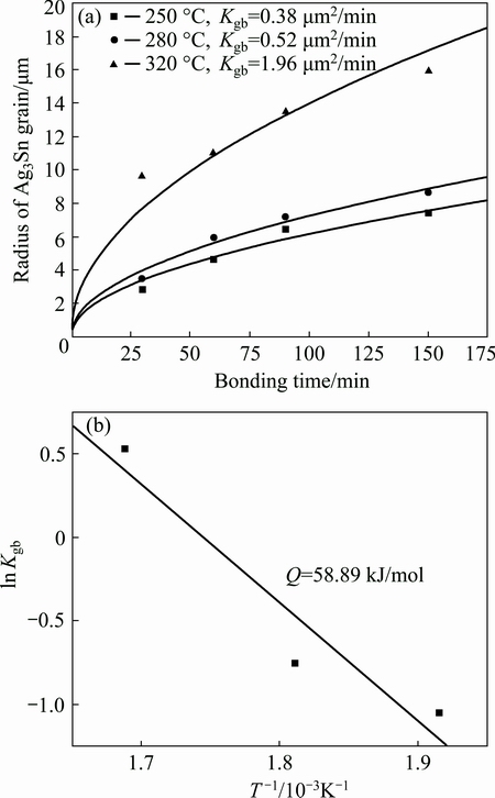
Fig. 8 Growth kinetic plots (a) and Arrhenius plot (b) for Ag/Sn system TLP soldering
4 Discussion
4.1 Mechanism of Ag3Sn growth
As can be seen, the scalloped Ag3Sn grains generally turn into more planar with dwell time, and the Sn/Ag3Sn interface becomes more flat, accordingly. This reveals evolution process in thickness direction of the IMCs during Ag-Sn TLP soldering. It was suggested that two factors influenced the growth rule, including grain coarsening and solid-liquid interfacial reaction. In detail, those Ag3Sn grains with same orientation would merge into a new larger one with the increase of soldering time, which reduced the number of the grain boundaries and changed dominant diffusion path of the Ag atoms from substrate, namely, from grain boundary diffusion to diffusion through the IMCs. Furthermore, different Ag fluxes for different positions on the surface of one Ag3Sn grain induced its anisotropic growth and decreased the curvature of the grain. In order to explain this phenomenon, a model of Ag flow for Ag3Sn grain growth was established (Fig. 9). In this theory, two grains with different sizes were selected, and it was assumed that Ag3Sn grain had a structure of hexagonal base and spherical cap in three dimensions referred to Ref. [31]. On one hand, grain coarsening could be explained by the Gibbs-Thomson effect [23], and the concentration of Ag atoms on the surface of the Ag3Sn grain was
 (7)
(7)
 (8)
(8)
where Cr is the concentration of Ag atoms at the Ag3Sn/Sn interface, C0 is the equilibrium concentration of Ag atoms in the molten Sn, �� is the interfacial energy per unit area between Ag3Sn and Sn, Vm is the molar volume of Ag3Sn compound, and r is the radius of Ag3Sn spherical cap. Due to the curvature difference, the concentration gradient of Ag was set up in the molten Sn between grains with different radii. That caused a flux of Ag atoms from the small-sized grain to the big-sized one, which could be expressed by [23]
 (9)
(9)
where Jr is the Ag flux for grain coarsening, DA is the diffusion coefficient of Ag atoms into molten Sn, ��gb is the space between two Ag3Sn grains,  is the average radius of the small-sized grains neighboring the big-sized one. This ripening flux of Ag atoms made the small grain merge into the larger one until the grain boundary disappeared. It was worth mentioning that grain coarsening process was observed with a top-view SEM image of the IMCs in our work. As shown in Fig. 10, several original Ag3Sn scallops had been swallowed by the larger grain and formed a new bigger irregular- shaped grain; however, their original grain boundaries still remained on the surface of the new one that seemed necking structures. If continued to grow, these structures would gradually vanish and the surface of the new grain turned into smooth.
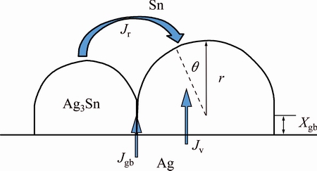
Fig. 9 Schematic diagram of Ag flux for Ag3Sn grain growth
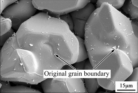

Fig. 10 Grain coarsening by means of merging into bigger grains
On the other hand, Ag flux from the substrate would prompt interfacial reaction and made the layered Ag3Sn turn into more planar. The Ag atoms could pass through the thick laminar IMCs layer with two diffusion channels as mentioned above. When many grains existed in the IMCs layer, grain boundary diffusion was the dominant control mechanism; however, this process declined with soldering time, especially for the thick IMCs layer. The Ag flux diffused along grain boundary could be described as [32]
 (10)
(10)
where Jgb is the Ag flux along grain boundary, xgb is the average diffusion distance along grain boundary, �� is a geometric parameter, ��gb is the average thickness of the grain boundary, Dgb is the diffusion rate of Ag atoms at the grain boundary, ��C is the homogeneity range of Ag3Sn,  is the average height of the Ag3Sn grain, and �� is a geometrical correction factor correlating the and xgb. From this equation, Ag flux controlled by grain boundary diffusion reduced with soldering time due to increase of the thickness of the IMCs layer, and decrease of the number of the grain boundaries caused by grain coarsening also had negative effect on Ag diffusivity along this channel. And then, diffusion through IMCs (volume diffusion) became the dominant mechanism that controlled the Ag3Sn growth. According to the Fick��s first law, Ag flux diffusion through the Ag3Sn grain was estimated as follows:
 (11)
(11)
where Jv is the Ag flux through Ag3Sn grain, D�� is the diffusion coefficient of Ag atoms in Ag3Sn crystal, �� is the angle between radial direction of one position on the spherical cap and vertical direction of the substrate, Cs is the equilibrium concentration of Ag atoms at the Ag/Ag3Sn interface, Cr is the concentration of Ag atoms at the Ag3Sn/Sn interface, and r is the radius of the spherical cap. This equation indicated that Ag flux increased with the increasing �� value. Therefore, growth velocity at root of the Ag3Sn spherical cap was faster than that of the top, which caused that Ag3Sn scallop gradually evolved into more planar.
4.2 Mechanism of nano-particles formation
As mentioned above, abundant nano-particles formed on the surface of Ag3Sn grains. Figure 11 showed the magnified morphology, these nano-particles had slight agglomeration for their quite high surface energy, and were dispersedly distributed on the IMCs surface. According to the EDS results (Table 2), Sn contents of the different particle phases were lower than that of the Ag3Sn with 25% Sn. However, nano-particles grew in the molten Sn in our study, and the concentration of Sn atoms on the surface of particles must be very high even reached the eutectic composition. It was quite difficult that particle phase transformed into �� phase or (Ag) under this condition according to Ag-Sn phase diagram. Therefore, we considered that nano-particle should be Ag3Sn phase. Furthermore, it was clearly found that the interfacial angle between nano-particle and Ag3Sn grain was lower than 90��, which indicated that those particles were not crystal nucleuses based on the IMCs. It was supposed that nano-particles might be formed in molten Sn where Ag atoms had segregation driven by thermodynamics, and process of them attached to Ag3Sn grains possibly occurred in the solidification.
On one hand, Ag-rich areas caused by the segregation of Ag atoms were benefit to the nucleation of nano-Ag3Sn particles. According to the theory of nucleation dynamics, nucleation rate can be described by [33]
 (12)
(12)
where I is the nucleation rate, �� is the vibration frequency of Ag atoms in the liquid, NS is the number of Ag atoms on the surface of the critical nucleus, p is the possibility of Ag atoms accepted by the critical nucleus, NL is the number of Ag atoms in per unit volume of the liquid, ��G is the activation energy for the nucleation of a critical number of the clustered atoms, ��G* is the activation free energy for diffusion through solid/liquid interface, kB is Boltzman��s constant. From Eq. (12), Ag-rich area meant a great deal of Ag atoms in per unit volume of the liquid, which promoted nucleation of the Ag3Sn and amount of nano-particles formed in the molten Sn.
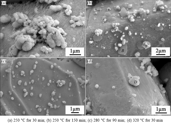
Fig. 11 Nano-particles formed on surface of Ag3Sn scallops
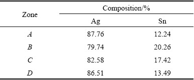
Table 2 EDS analysis results of indicated zone in Fig. 11
On the other hand, the phenomenon that nano- Ag3Sn particles were precipitated on the Ag3Sn grains could be explained by the minimum energy principle. Since nano-Ag3Sn particles located in the liquid were unstable for their quite high surface free energy, agglomeration would take place and adsorption to Ag3Sn grains occurred during solicitation process so as to decrease the surface free energy. If we considered the nano-Ag3Sn particle as active material and the Ag3Sn grain as big plane, Gibbs adsorption theory could be used to describe this phenomenon. The adsorption amount of active material on the crystal plane K can be given by [25-27]
 (13)
(13)
where ��K is the adsorption amount of surface active material at plane K, C is the concentration of surface active material, and ��K is the surface tension of plane K. Furthermore, the surface free energy of the system can be expressed as follows:
GK=��KAK (14)
where AK is the area of the plane K.
According to Eq. (13) and Eq. (14), the change of surface energy with the concentration at a given temperature depends on the adsorption of active material. However, concentration of the interface in a stable system is constant, the minimum the free energy is, the maximum the adsorption amount will be. In other words, adsorption of nano-Ag3Sn particles on the surface of Ag3Sn grains was prone to occurring in this condition. YU et al [27] supposed that this process would decrease the surface free energy of the system and make it more stable.
5 Conclusions
1) Morphologies of Ag3Sn grains majorly were scallop-type, and some other shapes such as prism, needle, hollow column, sheet and wire of Ag3Sn crystals were also observed, which resulted from the anisotropic growth of the IMCs grains. The prism-type Ag3Sn grain was more easily to be formed under higher soldering temperature, and the non-scalloped Ag3Sn generally appeared on the surface of the primary IMCs with large plane.
2) The scalloped Ag3Sn layer usually evolved into more planar with prolonging soldering time, which was attributed to grain coarsening and anisotropic fluxes of Ag atoms from substrate. It was found that grain coarsening took place by a means of boundary migration and disappearance.
3) A great deal of nano-Ag3Sn particles were observed on the surface of the Ag3Sn grains. It was supposed that these particles were nucleated in the Ag-rich areas and adsorbed by the Ag3Sn IMCs in solidification process.
4) Growth kinetics of the Ag3Sn grains in TLP soldering followed a parabolic relationship with soldering time, and the growth rate constants of 250, 280 and 320 ��C were 5.83��10-15, 7.83��10-15 and 2.83��10-14 m2/s, respectively. Accordingly, the activation energy of the reaction was estimated to be about 58.89 kJ/mol.
References
[1] JOHNSON R W, WANG C, LIU Y, SCOFIELD J D. Power device packaging technologies for extreme environments [J]. IEEE Transactions on Electronics Packaging Manufacturing, 2007, 30(3): 182-193.
[2] MANIKAM V R, CHEONG K Y. Die attach materials for high temperature applications: A review [J]. IEEE Transactions on Components Packaging & Manufacturing Technology, 2011, 1(4): 457-478.
[3] NEUDECK P G, OKOJIE R S, CHEN L Y. High-temperature electronics��A role for wide bandgap semiconductors? [J]. Proceedings of the IEEE, 2002, 90(6): 1065-1076.
[4] LIS A, LEINENBACH C. Effect of process and service conditions on TLP-bonded components with (Ag,Ni�C)Sn interlayer combinations [J]. Journal of Electronic Materials, 2015, 44(11): 4576-4588.
[5] BOSCO N S, ZOK F W. Critical interlayer thickness for transient liquid phase bonding in the Cu-Sn system [J]. Acta Materialia, 2004, 52(10): 2965-2972.
[6] SHEN J, CHAN Y C, LIU S Y. Growth mechanism of bulk Ag3Sn intermetallic compounds in Sn-Ag solder during solidification [J]. Intermetallics, 2008, 16(9): 1142-1148.
[7] LU H Y, BALKAN H, NG K Y S. Effect of Ag content on the microstructure development of Sn-Ag-Cu interconnects [J]. Journal of Materials Science: Materials in Electronics, 2006, 17(3): 171-178.
[8] CHANG S Y, JAIN C C, CHUANG T H, FENG L P, TSAO L C. Effect of addition of TiO2 nanoparticles on the microstructure, microhardness and interfacial reactions of Sn3.5AgXCu solder [J]. Materials & Design, 2011, 32(10): 4720-4727.
[9] TSAO L C, CHANG S Y, LEE C I, SUN W H, HUANG C H. Effects of nano-Al2O3 additions on microstructure development and hardness of Sn3.5Ag0.5Cu solder[J]. Materials & Design, 2010, 31(10): 4831-4835.
[10] GAIN A K, FOUZDER T, CHAN Y C, YUNG W K C. Microstructure, kinetic analysis and hardness of Sn-Ag-Cu-1wt% nano-ZrO2 composite solder on OSP-Cu pads [J]. Journal of Alloys and Compounds, 2011, 509(7): 3319-3325.
[11] LIN F, BI W, JU G, WANG W, WEI X. Evolution of Ag3Sn at Sn-3.0Ag-0.3Cu-0.05Cr/Cu joint interfaces during thermal aging [J]. Journal of Alloys and Compounds, 2011, 509(23): 6666-6672.
[12] LEE Y H, LEE H T. Shear strength and interfacial microstructure of Sn-Ag-xNi/Cu single shear lap solder joints [J]. Materials Science and Engineering A, 2007, 444(1-2): 75-83.
[13] LAW C M T, WU C M L, YU D Q, WANG L, LAI J K L. Microstructure, solderability, and growth of intermetallic compounds of Sn-Ag-Cu-RE lead-free solder alloys [J]. Journal of Electronic Materials, 2006, 35(1): 89-93.
[14] CHUANG T H, TSAO L C, CHUNG C H, CHANG S Y. Evolution of Ag3Sn compounds and microhardness of Sn3.5Ag0.5Cu nano-composite solders during different cooling rate and aging [J]. Materials & Design, 2012, 39: 475-483.
[15] LI Q, CHAN Y C. Growth kinetics of the Cu3Sn phase and void formation of sub-micrometre solder layers in Sn-Cu binary and Cu-Sn-Cu sandwich structures [J]. Journal of Alloys and Compounds, 2013, 567: 47-53.
[16] ZOU H F, YANG H J, ZHANG Z F. Morphologies, orientation relationships and evolution of Cu6Sn5 grains formed between molten Sn and Cu single crystals [J]. Acta Materialia, 2008, 56(11): 2649-2662.
[17] WANG P J, SHA C H, LEE C C. Silver microstructure control for fluxless bonding success using Ag-In system [J]. IEEE Transactions on Components & Packaging Technologies, 2010, 33(2): 462-469.
[18] ZOU H, ZHU Q, ZHANG Z. Growth kinetics of intermetallic compounds and tensile properties of Sn-Ag-Cu/Ag single crystal joint [J]. Journal of Alloys and Compounds, 2008, 461(1-2): 410-417.
[19] LI J F, AGYAKWA P A, JOHNSON C M. Kinetics of Ag3Sn growth in Ag-Sn-Ag system during transient liquid phase soldering process [J]. Acta Materialia, 2010, 58(9): 3429-3443.
[20] LIS A, PARK M S, ARROYAVE R, LEINENBACH C. Early stage growth characteristics of Ag3Sn intermetallic compounds during solid�Csolid and solid�Cliquid reactions in the Ag-Sn interlayer system: Experiments and simulations [J]. Journal of Alloys and Compounds, 2014, 617: 763-773.
[21] LIN C, JAO C, LEE C, YEN Y. The effect of non-reactive alloying elements on the growth kinetics of the intermetallic compound between liquid Sn-based eutectic solders and Ni substrates [J]. Journal of Alloys and Compounds, 2007, 440(1-2): 333-340.
[22] LI J F, AGYAKWA P A, JOHNSON C M. Interfacial reaction in Cu/Sn/Cu system during the transient liquid phase soldering process [J]. Acta Materialia, 2011, 59(3): 1198-1211.
[23] KIM H K, TU K N. Kinetic analysis of the soldering reaction between eutectic SnPb alloy and Cu accompanied by ripening [J]. Phys Rev B Condens Matter, 1996, 53(23): 16027-16034.
[24] GHOSH G. Dissolution and interfacial reactions of thin-film Ti/Ni/Ag metallizations in solder joints [J]. Acta Materialia, 2001, 49(14): 2609-2624.
[25] TSAO L C. Evolution of nano-Ag3Sn particle formation on Cu-Sn intermetallic compounds of Sn3.5Ag0.5Cu composite solder/Cu during soldering [J]. Journal of Alloys and Compounds, 2011, 509(5): 2326-2333.
[26] LIU X, HUANG M, ZHAO Y, WU C M L, WANG L. The adsorption of Ag3Sn nano-particles on Cu-Sn intermetallic compounds of Sn-3Ag-0.5Cu/Cu during soldering [J]. Journal of Alloys and Compounds, 2010, 492(1-2): 433-438.
[27] YU D Q, WANG L, WU C M L, LAW C M T. The formation of nano-Ag3Sn particles on the intermetallic compounds during wetting reaction [J]. Journal of Alloys and Compounds, 2005, 389(1-2): 153-158.
[28] LI B, SHI Y, LEI Y, GUO F, XIA Z, ZONG B. Effect of rare earth element addition on the microstructure of Sn-Ag-Cu solder joint [J]. Journal of Electronic Materials, 2005, 34(3): 217-224.
[29] TAIJI N. Thermodynamics of microstructure [M]. Beijing: Chemical Industry Press, 2006.
[30] TAIJIN N. Thermodynamics of microstructure [M]. Beijing. Chemical Industry Press, 2006.
[31] YU C, CHAN J, CHENG Z, HUANG Y, CHEN J, XU J, LU H. Fine grained Cu film promoting Kirkendall voiding at Cu3Sn/Cu interface [J]. Journal of Alloys and Compounds, 2016, 660: 80-84.
[32] SCHAEFER M, FOURNELLE R A, LIANG J. Theory for intermetallic phase growth between Cu and liquid Sn-Pb solder based on grain boundary diffusion control [J]. Journal of Electronic Materials, 1998, 27(11): 1167-1176.
[33] SHEN J, LIU Y C, GAO H X. In situ nanoparticulate-reinforced lead-free Sn-Ag composite prepared by rapid solidification [J]. Journal of Materials Science: Materials in Electronics, 2007, 18(4): 463-468.
Ag-Sn���¹���Һ��������Ag3Sn��������������
�ۻ���1,2,3���ⰮƼ1,2,3��������1,2,3���� �h1,3������1,3
1. �廪��ѧ ��е����ϵ������ 100084��
2. �廪��ѧ Ħ��ѧ�����ص�ʵ���ң����� 100084��
3. �廪��ѧ �Ƚ���������������ص�ʵ���ң����� 100084
ժ Ҫ�����¹���Һ��(TLP)������һ���ڿ������뵼�廥������Ӧ��DZ���ĸ��µ��ӷ�װ�����������о���Ag/Sn��ϵ�ڲ�ͬ�¶��½���TLP����ʱ��������仯����(IMCs)���������������������Ag3Sn������Ҫ���ȱ�״��̬��������״����״���п���״����״����״����̬Ҳ�������Ȼ�������ű���ʱ����ӳ�����״Sn/Ag3Sn���潫��ø���ƽ̹�������������뾧���ֻ�������Agԭ�Ӹ������Ե���ɢ���йأ�ͬʱ����Ag3Sn��������۲쵽��������Ag3Sn�����γɣ������κ˳�����Һ�Ag�����������̹����б�Ag3Sn���������������¡��ڶ���ѧ���棬Ag3Sn����������ѭ�����߹��ɣ���Ҫ�ܵ������ɢ���ƣ���250��280��320 ��C���������ʳ����ֱ�Ϊ5.83��10-15��7.83��10-15��2.83��10-14 m2/s����Ӧ���Ϊ58.89 kJ/mol��
�ؼ��ʣ�����Һ�����ӣ�Ag3Sn��������̬����������ѧ�����
(Edited by Yun-bin HE)
Foundation item: Project (51375260) supported by the National Natural Science Foundation of China
Corresponding author: Hua-kai SHAO; Tel: +86-10-62773859-5; E-mail: shk13@mails.tsinghua.edu.cn
DOI: 10.1016/S1003-6326(17)60080-3
Abstract: Transient liquid phase (TLP) bonding is a potential high-temperature (HT) electron packaging technology that is used in the interconnection of wide band-gap semiconductors. This study focused on the mechanism of intermetallic compounds (IMCs) evolution in Ag/Sn TLP soldering at different temperatures. Experimental results indicated that morphologies of Ag3Sn grains mainly were scallop-type, and some other shapes such as prism, needle, hollow column, sheet and wire of Ag3Sn grains were also observed, which was resulted from their anisotropic growths. However, the scallop-type Ag3Sn layer turned into more planar with prolonging soldering time, due to grain coarsening and anisotropic mass flow of Ag atoms from substrate. Furthermore, a great amount of nano-Ag3Sn particles were found on the surfaces of Ag3Sn grains, which were formed in Ag-rich areas of the molten Sn and adsorbed by the Ag3Sn grains during solidification process. Growth kinetics of the Ag3Sn IMCs in TLP soldering followed a parabolic relationship with soldering time, and the growth rate constants of 250, 280 and 320 ��C were calculated as 5.83��10-15 m2/s, 7.83��10-15 m2/s and 2.83��10-14 m2/s, respectively. Accordingly, the activation energy of the reaction was estimated about 58.89 kJ/mol.
