

Portable nano probe for micro/nano mechanical scratching and measuring
Woo-Park JEONG1, Chang-Choi SOO2, Cho HYUN3, Woo-Lee DEUG3
1. Department of Mechanical Design Engineering, Chosun University, Gwangju 501-759, Korea;
2. Department of Nano Fusion Technology, Pusan National University, Miryang 627-706, Korea;
3. Department of Nano-mechatronics Engineering, Pusan National University, Miryang 627-706, Korea
Received 21 April 2010; accepted 10 September 2010
Abstract:
A nano probe system which can measure precise micro parts or optical parts in nanometer range resolution and scratch contact force in mN scale was demonstrated. The nano probe was originally designed for on-machine measuring applications and one kind of contact type measuring probes was designed for miniaturized or microfactory system. It ideally should be of small size and able to measure surface topography in nanometer scale. A commercial capacitive displacement sensor was proposed. It was a new concept in nano probe systems which can measure the displacement of shaft driven by the variation of surface topography. The nano probe mainly consisted of three parts: a capacitive displacement sensor, a porous type air slide and a contact probe part with various tip radiuses. The porous type air slide assured the shaft slided smoothly with controllable normal force in mN scale and had high positioning accuracy. The probe part which was directly in contact with target surface, can be applied to micro/nanoscale scratching as well as the measurement of sample topography by a simple tip change.
Key words:
nano probe; displacement sensor; air slide; PCD tip;
1 Introduction
According to current industrial trends, an accurate measuring system for fine dimensional metrology in nanometer scale is essential for a miniaturized and highly accurate coordinate measuring machine (CMM), especially in a miniaturized product system. In fine metrology, the miniaturization of these measuring systems is a critical hurdle when considering portable availability for on-machine measurement, high resolution and vibration problems, etc.
The key issues on fine measuring from micro to nano scale are summarized and shown in Fig.1. Basic concepts and research related to the miniaturized metrology system mainly focused on the following parameters: metrology frame design and manufacturing, positioning stage design and feed back control, probe sensor and environmental control for vibration and disturbances.
All the parameters mentioned above are necessary for high-resolution metrology; however, there are some restrictions for choosing specific mechanical elements since the shapes and dimensions of target parts are generally not fixed.
For universal use of a metrology system from micro to nano scale resolutions, CMM may have limitations in dimensional volume. Therefore, recent research focused on a portable nano sensor, which can achieve on-machine measurements on conventional precision machine tools. ENAMI et al[1] and TAKAMASU et al[2] developed a new concept nano probe using metal ball sensing through optical fiber and quadrant photo diode (QPD). OHMORI et al[3] introduced an ultra-precision sensor for 3D measurement system. In order to keep the probe compact, they used a compact laser distance-sensing device, which can be applied to the on-machine measurement on ultra precise machine tools owing to its simple structural design and miniaturized size. In the case of an on-machine measuring sensor, additional design or fabrication such as metrology frame, positioning stage and environmental control for vibration and disturbances are not needed because columns and stages are used on the high precision machine tool as a metrology base. In addition, the fabrication cost and process time can be reduced compared to an ultra precise CMM system. One of the disadvantages, however, is that the measuring resolution worsens regardless of the sensor resolution when the high precision machine tools can not follow up the desired resolution. Therefore, KAWASEGI et al[4] developed a mobile AFM to measure and scratch a sample substrate in nanometer scale with precise control of horizontal stages by PZT actuated movement, and to measure sample surface in nanometer resolution regardless of the spatial resolution of precision machine tools. TASHIRO et al[5] and HAYASHI et al[6] also introduced simple scratch apparatuses using load cell and capacitive displacement sensors, and achieved micro scale measuring and scratching on brittle sample with precise PZT control in plane X, Y direction. Recently, FAN et al[7-8] developed a low-cost micro-CMM for 3D micro/nano measurements using miniaturized displacement spindle system, which consisted of a mini linear diffraction grating interferometer (LDGI) and an optical focus probe. In addition, multiple cantilever sensors or commercial displacement sensors were introduced[9-12] to stabilize and suppress the noise level from outer disturbances on AFM or STM.

Fig.1 Schematic diagram of nano-scale measurement machine
In this work, a portable nano probe with a capacitive displacement sensor was introduced, to measure the longitudinal displacement variation of probe shaft, on which the ball stylus or pinpoint stylus was mounted. Micro scratching in mN order as well as on-machine measuring applications was demonstrated.
2 Design and fabrication
2.1 Concept and mechanism
The measuring mechanism of the nano probe sensor is illustrated in Fig.2. A probe shaft moves upwards or downwards according to the ball probe displacement which is determined by scanning along the sample surface. Then the installed capacitive displacement sensor (Series 2805; ADE technologies, resolution 10 nm, measuring range ��1 000 ?m) measures the transferred gap variation between probe shaft and sensor part. Finally, the topographical data of the sample substrate is visualized via the data acquisition system. Generally, any distance between the point of interest (sample surface) and the sensor introduces a position uncertainty due to the behavior of the ��material path�� or the uneven surface topography[13]. This uncertainty is almost inevitable in general direct distance sensing applications. As a result, the probe shaft is used as an indirect distance transferring unit. The sharp stylus is mounted at the end of the probe shaft to acquire the localized surface information. Hence, the position uncertainty can be minimized from a structural point of view. The sensor only measures the distance from a stable reference plate as illustrated in Fig.2.
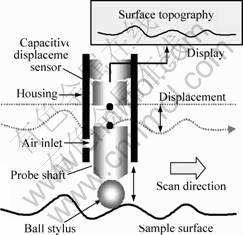
Fig.2 Schematic diagram of nano probe
This nano probe system can be used in scratching as well as measuring application by changing the ball probe for the lab-made diamond stylus probe. In addition, various types of tip radiuses or the material of probe stylus can be applied based on the sample characteristics.
Fig.3 illustrates the structural design and the fabricated nano probe system. To obtain accurate transfer displacement variations from the ball probe stylus, the probe shaft needs to slide in nanometer resolution.
Especially, this nano probe does not rotate or take high lateral forces between probe shaft and housing. In the case of measuring applications, the stylus probe tip should not leave scratch marks on the sample surface. Hence, relatively decreased normal contact force is required. For this reason, the air lubricated hydrostatic sliding mechanism is preferable owing to its negligible friction nature. This air slide provides low contact force to several mN scale, which is about 1/60 of that provided by the ball contact type sliding mechanism. To ensure stable and homogeneous pressure distribution along the radial direction of the probe shaft, a porous type air slide with tens of million submicron pores evenly spaced across the face is preferable. This porous air slide system has 44 N in the maximum radial load and 13 N/?m in radial stiffness.

Fig.3 Schematic diagram (a) and photo (b) of nano probe (Inset shows ball probe stylus for measuring)
2.2 Probe tips
As mentioned above, the nano probe can be applied to micro scratching in mN scale as well as on-machine measurements by changing probe tips. For those applications, the nano probe requires two types of probes: one is for measuring and the other is for scratching. The inset in Fig.3(b) shows the ball probe stylus (Reinshaw) for measuring surface topography, which is 300 ?m in diameter and made of ruby to provide hardness and wear resistance. To scratch or measure microelements, however, a probe tip with a sharp edge radius is preferable.
Previous research on micro/nano scratching called Tribo-Nanolithography (TNL) was based on AFM[14] and nanoindenter[15] which used commercial diamond grits (or tips) on a lab-made micro cantilever fabricated by MEMS process. For scratching applications, a lab-made diamond tip[16] was installed at the end of probe shaft. Fig.4 shows the SEM images of the fabricated silicon mold and diamond probe array. It can be seen from Fig.4(a) that the topography of the silicon mold has a pyramidal shape made by anisotropic etching. As shown in Fig.4(b), the quadrangular pyramid-shape diamond tip with 4 sharp cutting edges was accurately transferred from the silicon mold with dimensions of 100 ?m ��100 ?m��70 ?m[16]. In addition, the dimensions can be changed simply at the oxide patterning stage. The inset of Fig.4(b) shows the fabricated probe tip for scratching experiments or measuring micro elements. Fabricated diamond arrays are mechanically mounted and bonded by micromanipulator.

Fig.4 SEM images of fabricated silicon mold (a) and diamond probe array (b) (Inset shows fabricated probe tip for scratching or measuring micro elements)
3 Experimental
3.1 Analysis of sensing probe dynamics
To define the maximum contact force of probe within preferable lateral resolution, analysis of sensing probe dynamics was conducted as shown in Fig.5. When the stylus probe contacts the sample surface and the sample or nano probe moves along the scan direction, the friction force interacts on the top of the ball probe, which induces the X-directional displacements (L) of probe shaft. Then, the repulsive force (Fx) by the porous type air sliding to the radial direction starts to act on the probe shaft. It is necessary to reduce the X-directional displacement because it may cause a lateral error in measuring or machining. Thus, the contact force limit is calculated as follows:
![]() (1)
(1)
where ![]() .
.
To simplify the analysis in Eq.(1), it is assumed: the maximum sample inclination �� of 30��, friction coefficient ? of 0.3, X-directional displacements of probe shaft L of 10 nm and 50 nm, radial stiffness of 13 N/?m, no mechanical vibration on measuring stages and stable inlet air.

Fig.5 Simulation results of contact force limit according to probe shaft length and probe stylus displacements (Inset shows dynamics of sensing probe)
Assuming the probe shaft length is 50 mm and the acceptable X-directional displacements of the probe shaft are limited under 10 nm, and the maximum contact force Fy is roughly 122.509 mN (as shown in Fig.5) which means that longitudinal resolution can be guaranteed within 10 nm as long as the contact force does not exceed 122.509 mN. This lateral resolution should be precisely controlled due to its direct relationship with position uncertainty.
3.2 Application to micro/nano mechanical (100) silicon surface modification
The nano probe can be applied to studying micro scratching under mN scale normal forces. According to previous study[14], micro/nano scratching in ��N scale can be conducted by modifying the conventional AFM. However, it is known that the normal load is limited to several hundreds of ��N scale due to the cantilever stiffness. Recently, a nanoindenter-based scratch study[15] demonstrated that micromachining in mN scale is possible, while tool change, measuring application and portability are hardly possible.
The experimental set for scratching (100) silicon wafer is shown in Fig.6. All the scratching experiments in ��110? direction were observed by optical microscope. Simply, it can be known that the widths of scratch marks are in proportion with contact force and brittle material can be machined under 30 mN, as shown in Fig.7. It is seen that the micro crack on silicon surface starts at over 40 mN. Then the crack grows along the ��100? direction and finally breaks in bulk scale over 70 mN. Based on these experimental results, it can be concluded that the precise control of contact force has bright potential for the possibility of the mechanical micromachining on brittle materials. Further efforts on this application are underway.
Fig.6 Experimental set for scratching silicon wafer

Fig.7 Width variation of scratch marks on (100) Si wafer in ��110? direction according to contact force from 5 to 80 mN
4 Conclusions
In summary, a nano probe system that can scratch with mN scale normal force and measure precise micro parts in nanometer range vertical and lateral resolutions was introduced. A new concept in the nano probe system by applying a commercial capacitive displacement sensor was proposed, which can measure the displacement of probe shaft driven by the variation of surface topography. From a structural point of view, this minimizes the position uncertainty. To provide fine movement of probe shaft, a porous type air slide with stable pressure distribution was applied. Two types of stylus probes, ruby ball and PCD tip, were employed according to the specific applications. In addition, the precise control of contact force for fine machining and maximum force limit to determine lateral resolution were calculated both experimentally and numerically. From these basic experimental results, it can be concluded that the developed nano probe can be simply applied to both on-machine measurements and micro scratching in nano meter resolution under common environmental conditions.
References
[1] ENAMI K, HIRAKI M, Takamasu K. Nano-probe using optical sensing [C]//IMEKO-XVI World Congress. 2000: 345-348.
[2] Takamasu K, Chih-Che K, Suzuki A, Hiraki M, Furutani R, Ozono S. Development of pneumatic ball probe for measuring small hole [C]//International Conference on Precision Engineering. 1997: 767-771.
[3] Ohmori H, Uehara Y, Watanabe Y, Lin W. Micro-manufacturing system research and micro-sensor for measuring micro-parts [C]//1st Intelligent Microfactory System International Workshop. 2005: 26-32.
[4] Kawasegi N, Morita N, Takano N, Yamada S, Oyama T, Ashida K, Inagaki K, Saito J. Development of 3D nano-machining and measuring system [C]//JAIST International Symposium on Nano Technology. 2003: 38.
[5] Tashiro Y, Morita N, Kawasegi N, Takano N, Yamada S, Oyama T. A study on mirror-like grinding Mechanism for gallium arsenide (GaAs)-3rd report [C]//Conference Proceedings of JSPE. 2004: 145-146.
[6] Hayashi H, Morita N, Kawasegi N, Takano N, Yamada S, Oyama T. Development and applications of diamond array tool using silicon mold (2nd report)��Evaluation of tool performance in various processings[C]//Conference Proceedings of JSPE. 2004: 1091-1092.
[7] Fan K C, Fei Y T, Yu X F, Chen Y J, Wang W, Chen L F, Liu Y S. Development of a low-cost micro-CMM for 3D micro/nano measurements [J]. Measurement Science and Technology, 2006, 17(3): 524-532.
[8] Fan K C, Lai Z F, Wu P, Chen Y C, Chen Y, J?ger G. A displacement spindle in a micro/nano level [J]. Measurement Science and Technology, 2007, 18(6): 1710-1717.
[9] Sparks A W, Manalis S R. Atomic force microscopy with inherent disturbance suppression for nanostructure imaging [J]. Nanotechnology, 2006, 17: 1574-1579.
[10] Sparks A W, Manalis S R. Scanning probe microscopy with inherent disturbance suppression [J]. Applied Physics Letters, 2004, 85(17): 3929-3931.
[11] Altmann S M, Lenne P F, Heinrich H J K. Multiple sensor stabilization system for local probe microscopes [J]. Review of Scientific Instruments, 2001, 72(1): 142-150.
[12] Abe M, Sugimoto Y, Custance O, Morita S. Atom tracking for reproducible force spectroscopy at room temperature with non-contact atomic force microscopy [J]. Nanotechnology, 2005, 16(12): 3029-3034.
[13] Holman A E, Laman C D, Scholte P M L O, Heerens W Chr, Tuinstra F. A calibrated scanning tunneling microscope equipped with capacitive sensors [J]. Review of Scientific Instruments, 1996, 67(6): 2274-2280.
[14] Park J W, Kawasegi N, Lee D W, Morita N. Tribo- nanolithography of silicon in aqueous solution based on atomic force microscope [J]. Applied Physics Letters, 2004, 85(10): 1766-1768.
[15] Park J W, Lee C M, Choi S C, Kim Y W, Lee D W. Surface patterning for brittle amorphous material using nanoindenter-based mechanochemical nanofabrication [J]. Nanotechnology, 2008, 19: 085301.
[16] Park J W, Lee S S, So B S, Jung Y H, Kawasegi N, Morita N, Lee D W. Characteristics of mask layer on (1 0 0) silicon induced by tribo-nanolithography with diamond tip cantilevers based on AFM [J]. Journal of Materials Processing Technology, 2007, 187: 321-325.
Foundation item: Project supported by National Core Research Center (NCRC) and Chosun University, Korea
Corresponding author: Woo-Lee DEUG; E-mail: dwoolee@pusan.ac.kr
