
��ѧ�ƽ�����Ĥ��ſؽ���Ĺ�����
�� ��1 , ������1, ���Ϊ2
(1. ���ӿƼ���ѧ ������������ѧԺ, �ɶ� 610054;
2. ������ͨ��ѧ ��������ǿ�ȹ����ص�ʵ����, ���� 710049)
ժ Ҫ��
����ԭ����������X�����������о���Al2O3�����ϴſؽ���Au/NiCr/Ta������Ĥ�����ϻ�ѧ��AuĤ��������ò�� ����ȡ��Ͳ���Ӧ��, ����ſؽ���AuĤ�����˶Աȡ� �������: ͨ����ѧ�ƹ���������AuĤ�����˴ſؽ��䱡Ĥ��״���ṹ�������ص�, ����Ĥ�����������־ۺ�����, �ſؽ���AuĤ�Ŀ����ߴ�ԼΪ60nm, ��ѧ��AuĤ�ߴ�����ӵ�400nm����; ��ѧ�Ʊ�Ĥ�ڴſؽ��䱡Ĥ�����ϱ���ֲڶ�����, ��ѧ�ƹ��նԴſؽ��������Ĥ�ľ���ȡ����гм���, �������о���ȡ�����������ġ��Ŵ�����, ���Բ���Ӧ������һ���ĵ������á�
�ؼ���: �ſؽ���; ��ѧ��; ������Ĥ ��ͼ�����: TB43.1
���ױ�ʶ��: A
Relationship between plating and magnetron sputtering for metallic films
TANG Wu1, DENG Long-jiang1, XU Ke-wei2
(1. School of Microelectronic and Solid State Electronics,University of Electronic Science and Technology of China, Chengdu 610054, China;
2. State Key Laboratory for Mechanical Behavior of Materials,Xi��an Jiaotong University, Xi��an 710049, China)
Abstract: Au/NiCr/Ta multi-layered metal films were deposited on Al2O3 substrate by magnetron sputtering and then Au film was chemically plated. The crystal orientation, residual stress and surface morphology were investigated, and comparison was made between plating and magnetron sputtering technology by X-ray diffractrometry and atomic force microscopy. Au grain increases from 60 to 400nm after plating. The results indicate that the plating technology can inherit the crystal orientation from magnetron sputtering, enlarge the preferred orientation, and harmonize the residual stress. The surface roughness of Au films increases after plating.
Key words: magnetron sputtering; chemical plating; metallic films
��һЩ������;�ļ��ɵ�·��(�������ɵ�·), ������Ĥ��ʱ����Ҫ����������� ��ն�Ĥ�ĺ�Ƚϱ�, Ϊ���ٵ�������, ����ʹ������ĺ�ȴﵽ������ȵ�3~5���� ���, �轫��̺õĵ�·���ӵذ��û�ѧ�Ʒ����Ӻ�, ʹ������ﵽ����ĺ�ȡ� �����ɵ�·�еı�Ĥ�Ʊ����ո���Ĥ��ѧ���ܺ͵�ѧ���ܵ��о������һ��������, ���ڴſؽ��������Ĥ�������ٻ�ѧ��һ�������Ĥ, ����صı�Ĥ��ѧ���ܻᷢ��ʲô���ı仯?��������ƺ���δ��������ע��, ��Ӧ��ʵ���������ټ������� ���, �������߽���������о�, ���������ֱ�Ĥ�Ʊ����նԱ�Ĥ���ܵ�Ӱ�졣
1 ʵ��
1.1 ��ѧ�ƹ���
��ѧ��Ĥ��ָ����Һ�����û�ѧ��Ӧ���ߵ绯ѧ��Ӧ�ڻ�����ϱ��������Ĥ��һ�ּ����� ������������Һ�л�ԭ��������, ���/Һ��������������ͳ���, �乤��ԭ����ͼ1��ʾ��
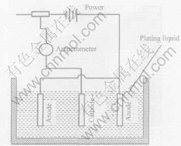
ͼ1 ��ѧ��Ĥ����ԭ��ʾ��ͼ
Fig.1 Schematic diagram of chemical plating
�Ƹ�������, ��Һ�еĽ������ӱ������ŵĶƲ��������, �����ϻ�ԭ��������������档 ��Ȼ, �������Ĵ������൱��Ҫ�� ���ڱ��еĢ������Ԫ�ؾ��л�ѧ������Ҫ�Ĵ�ЧӦ�� ���������IJ���, ������Ϊ�ĸ��Ӵ�����, �����ϡ� �մɡ� �����ȿ���ͨ���������������Ի, �����ڻ�ѧ��ԭ������
��ѧ�����û�ԭ���ĵ�λӦ�Ե��ڳ��������ĵ�λ�� ���õĻ�ԭ���д������κͼ�ȩ, ǰ����������, ����������ͭ�� ����, Ҳ���������⻯���Լ�������������������������������ԭ���� ����ʲô��ԭ��, �������ܹ����Դ����������ṩ�������ӻ�ԭ��Ԫ������Ҫ�ĵ��ӡ� ���ַ�Ӧֻ���ڴ������Ͻ���, ���, һ��������ʼ, ���������Ľ����ͱ����ܹ��������ִ�����, �Ա�������̲�����˶��жϡ� ������������, ��ѧ�Ʊ�Ȼ��һ���ܿص��Դ���ѧ��Ӧ���̡�
1.2 �����Ʊ�
Au/NiCr/Ta��Ĥ������VS-24C�ſؽ���������, �������ΪA99�������մ�Ƭ�� ���ν���Ta(50nm)�� NiCr(50nm)��Au(500nm)�� ϵͳ��ն�����10-4Pa, ��������Ϊ�ߴ������ ��100~250���ڸı�����¶�, ��ü�������, ���ͨ����ѧ�ƹ��ս�AuĤ������7��m��
1.3 ���Է���
��Rigaku/max-3C��X����������(Cu K��)��ⱡĤ������ṹ, ��ѹ40kV, ����35mA, ʯī��ɫ���˲�, ɨ�跶ΧΪ20��~85��; ��ԭ���������о���Ĥ������ò; Rigaku/MSF-2M��Ӧ�������Dz�����Ĥ����Ӧ��, ����sin2��[1], Cr K����, ��ѹ30kV, ����10mA, �˲�ƬΪ��, ���⾧��ΪAu(222)��
2 ���������
2.1 ������ò
ͼ2��ʾΪ�ſؽ���ͻ�ѧ��AuĤ��ԭ��������������ò�� ���Կ���, �ſؽ���Ĥ�Ŀ����ֲ�����, ��ֱ�ڱ������ϳ���״����, ��ѧ��Ĥ��, ���̳�����״�������ص���, �����䷢���˲��־ۺ�, ������С������ ͼ3��ʾ�����ſؽ���AuĤ�Ŀ����ߴ���60nm����, ��ѧ��AuĤ���Է����˿����ۺ�, ��ߴ�����ӵ�400nm���ҡ�
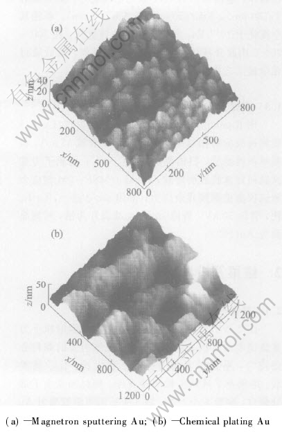
ͼ2 �ſؽ���ͻ�ѧ��AuĤ�������ά������ò
Fig.2 3D morphologies of magnetron sputtering and chemical plating Au film
���������Ĥ�����������뱡Ĥ���Ʊ����������й�ϵ[2-5]�� ����[6-9]�������������Ĥ�д�����״���ṹ�� ��״���ṹ����״�൱����, ����Ĥ�ܲ�������ѹ��Ӱ��, ����Ĥ�ܷŵ�����ѹ��Ӱ��, ��ѧ�Ʊ�Ĥ���ܻ��徧��ȡ��Ӱ�졣 �������Ʊ�Ĥ����״���ṹ�ڸ���ն��²�������[10], ��ʵ���н���ϵͳ��ն�����10-4Pa, ��ò�п��Թ۲쵽��״���ṹ, ���Ļ�ѧ��Ĥ�ڴ˻���������, �ṹδ�������仯��
ͼ4�Ƚ��˴ſؽ���ͻ�ѧ��Ĥ�ı���������, ���Կ���, ����Ĥ�Ŀ��������100~175nm֮��; ��ѧ��Ĥ�Ŀ��������80~200nm֮��, ˵����ѧ��Ĥ�ı���ֲڶ���Խϴ� ��Ȼ, ���뻯ѧ��Ĥ�ĺ��Զ���ڽ���Ĥ�кܴ��ϵ��
2.2 ����ȡ��
ͼ5��ʾΪ���ֹ����Ʊ���Ĥ��X���������ס� ��ͼ5��֪, �����Ǵſؽ��䱡Ĥ, �����ڴ˻����ϵĻ�ѧ�Ʊ�Ĥ, ��ֻ�۲쵽Au������塣 �����м�������������: Au(111)ȡ�����Au(111)��Au(200)ȡ���ǿ, Au(220)��Au(311)�����, ˵����Ĥ����֯��, ����ΪAu(111)����Au(111)��Au(200)���ȡ��
Au(111)��(200)ǿ�ȱ�ֵ��ͼ6��ʾ�� �ɼ�, ��ѧ�Ʊ�Ĥ��Ȼ����Au(111)����ȡ�� ��Ҫ�ر�ָ������, ����AuĤֻ��0.5��m��, ʣ������6.5��m��AuĤ��Ϊ��ѧ��, ����ѧ�ƹ��ն�4����Ʒ�Ǻ㶨�ġ� �������Ʋ�, 4�ֱ�Ĥ�ƺ���Ӧ���ھ���ȡ�����������졣 ��ʵ��, ͼ6�������, ��ѧ��AuĤ (111)��(200)���侧���ǿ�ȱ�ֵǿ�ҵ������ڡ���ס����������AuĤ�� �����¶ȴ�100�����ߵ�200���, ��ѧ��AuĤ����ǿ�ȱ�ֵ�ɴ�11.1�䵽3.6, ���������AuĤ(111)��(200)ǿ�ȱ�ֵԽ��, �ڴ˻����ϵĻ�ѧ��AuĤ(111)��������Խ������ �ɴ˿�֪��ѧ��Ĥ�ľ���ȡ��ǿ��������Ԥ�ȵĽ��乤��, ����ȡ���Ա����˴�ǰ����ʱ�����¶ȵ�Ӱ��, ��������������
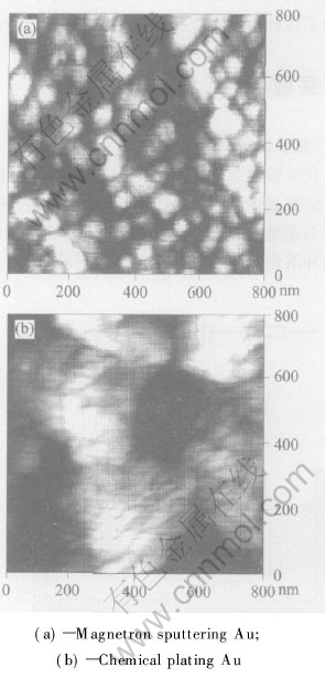
ͼ3 �ſؽ���ͻ�ѧ��AuĤ�Ķ�άƽ����ò
Fig.3 2D morphologies of magnetron sputtering and chemical plating Au film
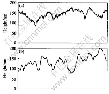
ͼ4 �ſؽ���AuĤ�ͻ�ѧ��AuĤ�ı������״̬�ֲ�ͼ
Fig.4 Grain height distribution curves of Au film by magnetron sputtering(a) and chemical plating(b)

ͼ5 �ſؽ���ͻ�ѧ��Au/NiCr/Ta��Ĥ��X����������
Fig.5 XRD patterns of Au/NiCr/Ta film by magnetron sputtering(a) and chemical plating(b)
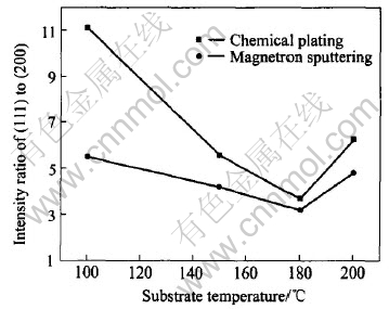
ͼ6 ��ͬ�����¶ȵ�Au(111)/(200)ǿ�ȱ�ֵ
Fig.6 Intensity ratio of Au(111) to (200) at different substrate temperatures
���ġ��Ŵ����á� ���������Ĥ�����ϵĻ�ѧ��Ĥ���к�ǿ����֯(��֯��)�м���, ������֯�м��ԶԱ�����Ϻϳ��������Ӱ��ֵ�ø����ر��ע��
2.3 ����Ӧ��
�ſؽ���ʹ˻����Ļ�ѧ��AuĤ����Ӧ���ֲ���ͼ7��ʾ��
ͼ7 �ſؽ���ͻ�ѧ��AuĤ�IJ���Ӧ��
Fig.7 Residual stress of Au film by magnetron sputtering and plating
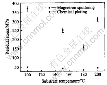
��ͼ7�ɼ�, �ſؽ��䱡Ĥ�IJ���Ӧ����150~400MPa��, ��ѧ�Ʊ�Ĥ�IJ���Ӧ��ά����40MPa����, ��������¶ȱ仯���� �����϶Դſؽ��������Ĥ�IJ���Ӧ��Ҳ����ر���[11-15], ������һ���ڼ���MPa�� ��ѧ�Ʊ�Ĥ����Ӧ��������¶ȱ仯����, ����������Ϊ��ԭ����ܲ�����Ϊ�¶ȷ�Χ�仯����, �Ͼ�����ȡ���Ѿ������˼���ı仯, ���ܵ������ǻ�ѧ�ƹ����б�Ĥ�����ϴſؽ����º�, �Ӷ��ı�������������ϵ�ƽ��Ӧ��״̬�� �ԱȲ���Ӧ���;���ȡ��Ľ��������Ϊ, ��ѧ�ƶԽ��䱡Ĥ�ľ���ȡ���н�ǿ�ijм���, ����Ӧ������һ���ĵ�������, ��Ϊ��Ӧ������������Ĥ/����ϵ�ϴﵽƽ�⡣ ��ʵ��, �������;���, �����ôſؽ����ȡ7��m��AuĤ��������, ��ʱ��Ĥ����Ӧ����ԶԶ�������в���ֵ, ���Ʊ������в��п���ʹ��Ĥ����������ѡ�
3 ����
1) ��ѧ��AuĤ�ڴſؽ�����״�������Ļ�������ṹδ�������仯��
2) ��ѧ�ƹ��նԴſؽ��������Ĥ�ľ���ȡ����гм���, �������������С��Ŵ����á�
3) ��ѧ�ƹ��նԴſؽ��䱡Ĥ����Ӧ����һ���ĵ������á�
REFERENCES
[1]Cullity B D. Elements of X-ray Diffraction[M]. Reagin: Addison-Wesley, 1978. 456-468.
[2]Mitsui A, Masumo K. Effect of a zirconium oxide undercoat on microstructure and properties of tin-doped indium oxide films for organic light emitting devices[J]. Thin Solid Films, 2003, 442(1-2): 140-144.
[3]Laha A, Bhattacharyya S, Krupanidhi S B. Impact of microstructure on dielectric properties of Pb(Mg1/3-Nb2/3)O3-PbTiO3 thin films[J]. Mater Sci Eng B, 2004, B106: 111-119.
[4]Cheng H E, Wen Y W. Correlation between process parameters, microstructure and hardness of titanium nitride films by chemical vapor deposition[J]. Surf Coat Technol, 2004, 179: 103-109.
[5]Brinkiene K, Kezelis R. Correlations between processing parameters and microstructure for YSZ films produced by plasma spray technique[J]. Journal of the European Ceramic Society, 2004, 24: 1095-1099.
[6]W��jcik W, Janczuk B, Bruque J M, The destruction time of the sediment column structure as a method for studying the dispersion system[J]. Powder Technol, 2000, 113: 1-8.
[7]Jobin M, Burdet B, Escudeiro S A, et al. AFM of ion-etched cross-sections: a method for analyzing the morphology of dense hard coatings[J]. Thin Solid Films, 2004, 469-470: 398-403.
[8]Santana A E, Karimi A, Derflinger V H, et al. Microstructure and mechanical behavior of TiAlCrN multilayer thin films[J]. Surf Coat Technol, 2004, 177-178: 334-340.
[9]Kim G, Lee S, Hahn J. Properties of TiAlN coatings synthesized by closed-field unbalanced magnetron sputtering[J]. Surf Coat Technol, 2005, 193: 213-218.
[10]Mayadas A F, Shatzkes M. Electrical resistivity model for polycrystalline films: the case of arbitrary reflection at external surface[J]. Phys Rev B, 1970, B1: 1382-1387.
[11]Nix W D. Mechanical properties of thin films[J]. Metal Trans A, 1989, A20: 2217-2249.
[12]Koski K, Holsa J, Juliet P. Properties of zirconium oxide thin films deposited by pulsed reactive magnetron sputtering[J]. Surf Coat Technol, 1999, 120-121: 303-312.
[13]Gillet M, Assaban A, Mikaelian G. Stress in thin Au films on �� alumina[J]. Vacuum, 1998, 50: 73-78.
[14]Pauleau Y. Generation and evolution of residual stresses in physical vapor-deposited thin films[J]. Vacuum, 2001, 61: 175-181.
[15]Tang W, Xu K, Wang P, et al. Residual stress and crystal orientation in magnetron sputtering Au films[J]. Mater Lett, 2003, 57: 3101-3106.
������Ŀ: ������Ȼ��ѧ�����ص�������Ŀ(59931010); �Ƽ����з��Ƚ��о��ƻ�������Ŀ(PRA MX9906)
�ո�����: 2005-07-15; ������: 2005-08-20
�����: �� ��(1975-), ��, ������, ��ʿ
ͨѶ����: �� ��; �绰: 028-83204938; E-mail: tangwu@mailst.xjtu.edu.cn
