
J. Cent. South Univ. (2012) 19: 2425-2433
DOI: 10.1007/s11771-012-1292-y![]()
Spectra analysis and O2 evolution for TiO2 photocatalyst compounded with indirect transition semiconductors
TONG Hai-xia(ͯ��ϼ)1,2, CHAI Li-yuan(����Ԫ)1, ZHANG Xin-rui(��ܰ�)2
1. School of Metallurgical Science and Engineering, Central South University, Changsha 410083, China;
2. College of Chemistry and Biology Engineering, Changsha University of Science and Technology, Changsha 410114, China
? Central South University Press and Springer-Verlag Berlin Heidelberg 2012
Abstract:
The photo absorbing, photo transmitting and photoluminescence performances of TiO2 photocatalysts compounded with V2O5 or WO3 were investigated by UV-Vis spectra, transmitting spectra, and PL spectra, respectively. The energy band structures of TiO2 photocatalysts were analyzed. The photocatalytic activities of the TiO2 photocatalysts were investigated by splitting of water for O2 evolution. The results indicate that the band gaps of WO3 and V2O5 are about 2.8 and 2.14 eV, respectively, and the band gap of rutile TiO2 is about 3.08 eV. Speeds of water splitting for 2%WO3-TiO2 and 8%V2O5-TiO2 photocatalysts are 420 and 110 ��mol/(L��h), respectively, under UV light irradiation. V2O5 and WO3 compounded with suitable concentration can improve the photocatalytic activity of TiO2 with Fe3+ as electron acceptor.
Key words:
1 Introduction
Low photoactivity and slow photolysis speed make TiO2 photocatalysts very difficult to be practically used. There are various methods for improving the efficiency of separation between photoelectrons and holes. However, at present, semiconductor compounding is considered as one of the most effective ways. For example, the band gap of CdS is about 2.4 eV, and it has high photocatalytic activity when being compounded with TiO2. The reactions are as follows [1]:
CdS+h�ԡ�![]() +
+![]() (1)
(1)
![]() +OH-��1/2
+OH-��1/2![]() +H+ (2)
+H+ (2)
![]() +H+��1/2H2 (3)
+H+��1/2H2 (3)
Regrettably, reaction (4) often takes the place of reaction (2), which leads to the light corrosion:
2![]() +CdS��Cd2++S (4)
+CdS��Cd2++S (4)
Therefore, besides considering the high photocatalytic activities and matched band structure of the semiconductor photocatalyst, other factors should be taken into account, such as the light corrosion in the process of photoreaction, and the stabilization (the pH range of its existence) in photocatalytic system. Nowadays, many studies have been focused on the study of the theory of the indirect transition semiconductor [2-5], and electronic, optical adsorption and magnetic properties [6-7]. However, the application of indirect transition semiconductor compounded with TiO2 has seldom been reported. Considering the band structure, photocatalytic activities and chemistry stabilization, WO3 and V2O5 were chosen to compound with rutile TiO2. WO3 and V2O5 are indirect band gap semiconductors. In order to investigate methods of improving the photocatalytic performance of semiconductors, TiO2 photocatalysts compounded with different amounts of WO3 and V2O5 were employed to split water for O2 evolution with Fe3+ as electron acceptor.
2 Experimental
2.1 Preparation of compounded TiO2 photocatalysts
Rutile TiO2 photocatalysts compounded with different amounts of WO3 and V2O5 were prepared according to our previous works [8-9]. A series of WO3-TiO2 catalysts were obtained with 1.33%, 2%, 2.67%, 5.33% and 10% (molar fraction) of WO3, and titled by T1, T2, T3, T4 and T5, respectively. Similarly, a series of V2O5-TiO2 catalysts with different V2O5 contents (molar fraction) of 5%, 8%, 10%, 20% and 40% were titled by V1, V2, V3, V4 and V5, respectively. Pure rutile TiO2 is titled by T0.
2.2 Characterization of compounded TiO2 photocatalysts
Diffusion reflectance UV-Vis spectra (UV-DRS) measurements were carried out on a Beijing Purkinje TU-1901 UV/Vis spectrophotometer equipped by a diffuse reflectance accessory with an IS19-1 integrating sphere, and BaSO4 powder was used as reference.
Transmissivity spectra measurements were carried out on a HITACHI-U4500 spectrophotometer, and the catalysts kept suspension in water with the mass fraction of about 1.7%.
To reveal the influence of the separation of charge carriers and surface structure, the photoluminescence measurements were carried on a HITACHI-F4500 fluorescent spectrometer, and the width of the slit is 5 ��m. The voltage of the photomultiplier tube is 700 V. The scanning-velocity is 1 200 nm/min.
The O2 evolution was detected by HATCHI SP-2305 gas chromatography equipped with a thermal conductivity detector. The argon was used as the carrier gas and the fixed phase is molecule sieve (5 ?).
2.3 Photoactivity tests
The photocatalytic reaction was performed using a closed gas-circulating system with an inner irradiation reactor. A light source (250 W high-pressure Hg lamp) was covered with a glass jacket made of quartz (cut-off wave length <200 nm). The reactor temperature was kept constant at 293 K using cooling water. A mixture of catalyst (2 g), distilled water (640 mL) and a required amount of Fe2(SO4)3 in the reactor was completely degassed, and then argon gas was introduced into the system. The catalyst powder was suspended by using a magnetic stirrer. The product gas oppressed the liquid in the reactor into the graduated cylinder through the outlet. So the volume of product gas can be read through the graduated cylinder indirectly. The evolution of O2 was detected by gas chromatography.
3 Results and discussion
3.1 UV-Vis absorption performance of compounded TiO2 photocatalysts
The UV-Vis diffuse reflectance spectra of T1, T2, T3, T4 and T5 are shown in Fig. 1. From Fig. 1, the reflectance of each TiO2 photocatalyst is basically similar in the wavelength range of 200-420 nm, which indicates that the difference of light absorption performance is minute in UV region. In the wavelength range of 420-700 nm, the reflectances of samples T1, T2, T3 and T4 also have no obvious difference. Contents of compounding WO3 are similar, so the diffuse reflectance UV-Vis spectra have little difference. When the content increases to 10% (T5), the absorption threshold expands to around 440 nm. Therefore, WO3 compounding can expand the wavelength range of TiO2 photocatalyst limitedly. According to ��g=1 240/Eg [10], the band gap of T5 is about 2.8 eV. The diffuse reflection spectra of compounding V2O5-TiO2 photocatalysts are shown in Fig. 2. From Fig. 2, an obvious absorption band can be seen in the wavelength range of 200-380 nm. It is the characteristic absorption of the charge transfer of O 2p��Ti 3d, and the charge is from oxygen atom coordinated with titanium to the empty orbit of the center titanium atom [11]. The absorption band in the wavelength range of 200-600 nm results from electron transition of O 2p��V 3d, the absorption band in the wavelength range of 400-480 nm results from electron transition of octahedron coordinate vanadium, and the absorption band in the wavelength range of 300-350 nm results from electron transition of tetrahedron coordinate vanadium. But the absorption band in the wavelength range of 200-300 nm is from utterly isolated octahedron vanadium. Therefore, the absorption band in the wavelength range of 200-350 nm should be attributed to the charges transition interaction between O 2p��Ti 3d and O 2p��V 3d [12]. According to Fig. 2, the absorption of visible light for V2O5-TiO2 catalysts is enhanced obviously. So V2O5 compounding can improve the absorption of visible light for TiO2 photocatalyst markedly.
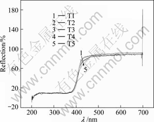
Fig. 1 Diffuse reflection spectra of compounded WO3-TiO2 photocatalysts

Fig. 2 Diffuse reflection spectra of compounded V2O5-TiO2 photocatalysts
3.2 UV-Vis transmittance performance of compounded TiO2 photocatalysts
Figure 3 shows the transmittance spectra of the suspending liquid of WO3-TiO2 photocatalyst powders. In the wavelength range of 200-410 nm, the transmittance of WO3-TiO2 increases gradually, it keeps constant in the range of 410-540 nm, and then decreases gradually after 540 nm. When the content of the compounded WO3 is 2%, it reaches the peak, where the transmittance is more than 50%. What��s more, the transmittances of other four samples reduce slowly with the increase of the content of the compounded WO3.
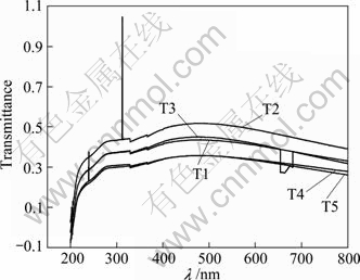
Fig. 3 Uv-Vis transmissivity of compounded WO3-TiO2 catalysts
Figure 4 shows the transmittance spectra of the suspending liquid of TiO2 powder with different V2O5 compounding. It is clear from the transmittance curves that with the increase of the content of compounded V2O5, the optical transmittance gradually decreases. The average transmittance in the visible region is larger than that in the UV-light region for all samples, and the transmission in the UV-light region is less than 5%. This means that all catalysts can absorb almost all the UV-light in the photocatalytic reactions according to UV-DRS in Fig. 2 and the transmitted spectra of the suspending liquid of V2O5-TiO2 catalysts in Fig. 4. In the wavelength region of 400-580 nm, for all the samples, the refraction and the transmittance increase gradually. This indicates that the catalysts can absorb visible light. But obviously, when the red shift of the wavelength occurs, the absorption will decrease. That is to say, the catalysts have a good absorption to UV-light and can also absorb visible light. But the transmittance does not change obviously with the increase of compounded V2O5.
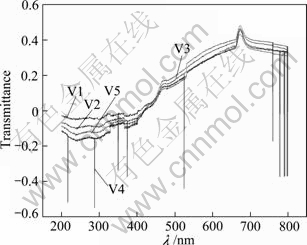
Fig. 4 Uv-Vis transmissivity of compounded V2O5-TiO2 catalysts
Under the illumination, the transition for electrons absorbing photons must keep conservation of momentum besides conservation of energy, which satisfies the selection rule. It is assumed that the primary wave vector of the electron is K, which will transit to the state with wave vector of K��. As for electrons in the energy band, hK is similar to the property of momentum, so during the process of transition, K and K�� must satisfy the conditions as follows [11]:
hK��-hK=M (5)
where M denotes the momentum of photons.
Generally, as the momentum of photons resulting from semiconductor absorbing is less than that of the electrons, the momentum of photons can be ignored. So Eq. (5) can be written as
K��=K (6)
This shows that the wave vector of electrons keeps equal after absorbing photon and the energy of electrons increases, which is the selection rule of electrons. In order to satisfy the selection rule and keep the wave vector constant during the transition, electrons in valence band in excited state A can only transit to state B in the conduction band. Because of states A and B on the same droop line in one-dimensional energy curve, this kind of transition is called direct transition. The intrinsic absorption of semiconductor forms a continuous absorption band, and has a long wave absorption edge ��0=Eg/h. So the band gap of semiconductor (Eg) can be extracted from the measurement of absorption.
The common semiconductors such as GaAs and InSb in III-V and II-VI subgroups are called direct gap band semiconductors because their minimum conduct band and maximum valence band are corresponding to the same wave vector. Theoretical calculation of electrons of this kind of semiconductors from their intrinsic absorption shows that if the transition for any K is permitted in the direct transition, the relationship between the absorption coefficient and photon energy can be denoted as [13]
![]() (7)
(7)
where �� is the absorption coefficient, and the relationship between �� and transmissivity T is ��=��-lnT; hv is the energy of photon with 1 240/��; A is a constant.
But both theory and experiment prove that the conduct bands and valence bands for many semiconductors such as Ge and Si are not corresponding to the same wave vector, which are called indirect gap semiconductors. For indirect semiconductors, the relationship between the absorption coefficient and photon energy is
![]() (8)
(8)
WO3 is an indirect gap semiconductor [14], so it can be calculated according to Eq. (8). The curves of (��hv)1/2 vs hv are shown in Fig. 5(a). The linear parts of the curves are extended to the point of ��=0, and the intercept on abscissa is the band gap (Eg). From Fig. 5(a), the band gap of the catalysts of 2%WO3-TiO2 is about 2.78 eV, which is in a good agreement with UV-Vis absorption spectrum. Rutile TiO2 is a direct gap semiconductor, and according to Eq. (7) and Fig. 5(b), the optical energy band gap of rutile TiO2 is about 3.08 eV.
V2O5 is an indirect gap semiconductor [15]. According to Eq. (8) and Fig. 6, the optical energy band gap of 8%V2O5-TiO2 is 2.14 eV.
3.3 Photoluminescence performance of compounded TiO2 photocatalysts
3.3.1 Photoluminescence performance of WO3-TiO2 photocatalysts
Figure 7 shows the FL spectra of WO3-TiO2 photocatalysts excited by 300 nm light, and the lights whose wavelength is lower than 350 nm are cut off. From Fig. 7, it can be seen that WO3 compounding has not led to the generation of a new photoluminescence peak. And along with the change of the content of the compounded WO3, the intensities of FL spectra have changed. In the FL spectra, TiO2 shows a strong and wide luminous signal in the wavelength range of 400-600 nm, and the positions of the peaks are near to 421, 470 and 536 nm, respectively. The luminescence band near 421 nm is probably attributed to free excitons emission [16], and bands near 470 and 536 nm may result from bound excitons emission [17], which may root in the imperfection of particle crystallization, such as the bound state from the distortion of crystal lattice. Because TiO2 catalysts have been treated at high temperature, which can result in many oxygen vacancies in the interface, the formation probability of the exciton bound by the hole is larger than that of normal materials. Thus, the exciton energy level will be formed near the bottom of the conduction band, and the exciton luminous band is formed too. Other fine structures of the luminous band may correspond to the interaction of electrons and phonons caused by multi-phonon optical transition [18]. The order of luminous intensity of WO3-TiO2 photocatalysts is 1.33%WO3-TiO2��2%WO3-TiO2>
2.67%WO3-TiO2>5.33%WO3-TiO2>10%WO3-TiO2, because of the decrease of the illuminated area of TiO2 with the increase of the compounded WO3 content. On the other hand, WO3 compounding may lead to the decrease of the concentration of oxygen vacancies on the surface of TiO2.
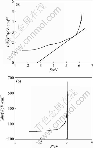
Fig. 5 Absorption coefficients as function of incident photo energy of catalysts: (a) 2%WO3-TiO2; (b) Rutile TiO2
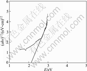
Fig. 6 Absorption coefficient as function of incident photo energy of 8%V2O5-TiO2 catalysts
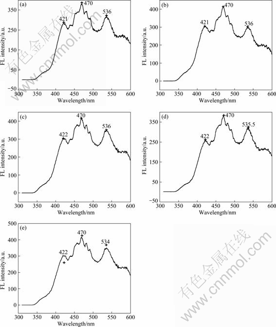
Fig. 7 Fluorescence spectra of compounded WO3-TiO2 photo catalysts excited by 300 nm light: (a) 1.33% WO3-TiO2; (b) 2% WO3-TiO2; (c) 2.67% WO3-TiO2; (d) 5.33% WO3-TiO2; (e) 10% WO3-TiO2
The photoluminescence spectra of TiO2 are related with the preparation conditions. That is to say, TiO2 may have various luminescence bands when using different preparation methods. This is because different preparation environment, such as temperature, pressure, purity of dopant, and growth methods, may affect the crystal structure, defects, shape of TiO2 greatly, which will influence the photoluminescence performance of TiO2 directly or indirectly [19-21].
3.3.2 Photoluminescence performance of V2O5-TiO2 photocatalysts
Figure 8 shows the photoluminescence spectra of compounded V2O5-TiO2 photocatalysts excited by 300 nm light. Compounded V2O5-TiO2 photocatalysts show strong and wide luminous signals in the wavelength range of 400-600 nm. The positions of peaks are 422, 471 and 537 nm, respectively. The order of luminous intensity of V2O5-TiO2 photocatalysts is 5%V2O5-TiO2 > 8%V2O5-TiO2 > 10%V2O5-TiO2 > 20% V2O5-TiO2 > 40%V2O5-TiO2.
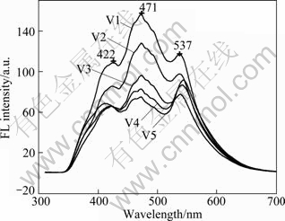
Fig. 8 Fluorescence spectra of compounded V2O5-TiO2 photocatalysts excited by 300 nm light
3.3.3 Comparison of photoluminescence performance among TiO2, 2%WO3-TiO2 and 8%V2O5- TiO2
Figure 9 shows the fluorescence spectra of TiO2, 2%WO3-TiO2 and 8%V2O5-TiO2 excited by 300 nm light. The order of FL intensity is TiO2 > 2%WO3-TiO2 > 8%V2O5-TiO2. Compared with pure TiO2, there is no new FL peak with WO3 and V2O5 compounding. But the peak shape of 8%V2O5-TiO2 is quite different from others. This is because the peak positions of TiO2 are near to 470 and 536 nm, which are similar to those of WO3 (474 and 535.5 nm), so the peak shape remains unchanged after being stacked. Overall, there are different discrete energy levels existing in conduction band of semiconductor, and different exciting energies can excite electrons to different levels. Electrons with different energies will emit fluorescence in different ways. As shown in Fig. 10 [22]. The mechanism of photoluminescence of semiconductors is very complex and needs further study. However, there is no change in peak position on FL spectra, which indicates that there are some relatively stable excitons or surface energy state in the surface of the semiconductor particles. Excitons are generated by the bound electrons, and there are oxygen vacancies in the surface of TiO2. At the same time, the particle size is small, and the average-free-paths of electrons are short. So oxygen vacancies are easier to change into excitons than bound electrons. As a result, it can form exciton energy levels in the band gap near the bottom of conduction band, and generate an exciton emission band, as shown in Fig. 10. Generally speaking, the higher the content of oxygen vacancies, the greater the probability of excitons generated by the bound photoelectrons, and the stronger the luminous signal of excitons [22]. Of course, not all oxygen vacancies can trigger excitons to illuminate. Oxygen vacancies, which can trigger luminescence, can inevitably influence the process of separation and recombination of photo-carriers strongly. After investigating the relationship between photoluminescence performance and photoactivity of ZnO and TiO2, JING et al [23] concluded that the stronger the fluorescence signal, the higher the concentration of surface oxygen vacancies and the higher the activities of photocatalytic oxidation of organic pollutants. But the conclusion is not suited for the compounding WO3-TiO2 and V2O5-TiO2 catalyst photolysis of water system in this work. So there are many factors that can influence the rate of O2 evolution of TiO2 catalyst and the photoluminescence performance is not the decisive one.
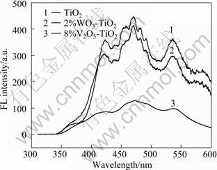
Fig. 9 Fluorescence spectra of TiO2, 2%WO3-TiO2 and 8%V2O5-TiO2 excited by 300 nm light
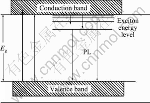
Fig. 10 Schematic diagram of occurrence of exciton luminescence band of semi-conductor nanoparticles
3.4 Splitting water for O2 evolution of compounded TiO2 photocatalysts
3.4.1 Splitting of water for O2 evolution of compounded WO3-TiO2 photocatalysts
Figure 11 shows the dependence of O2 evolution and the time of photo irradiation for the compounded WO3-TiO2 photocatalysts. The results show that the rate of O2 evolution of TiO2 compounded with WO3 is larger than that of the pure rutile TiO2 during 12 h. With the increase of the content of compounded WO3, the rate of O2 evolution also increases, and it reaches the maximum of 420 ��mol/(L��h) when the content of compounded WO3 is 2%. The rate of O2 evolution declines when the content of compounded WO3 is more than 2.67%.
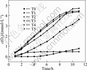
Fig. 11 Dependence of O2 evolution on time of photo irradiation for compounded WO3-TiO2 photocatalysts
3.4.2 Splitting of water for O2 evolution of compounded V2O5-TiO2 photocatalysts
From Fig. 12, the rate of O2 evolution of TiO2 compounded with V2O5 is larger than that of the pure rutile TiO2 during 12 h. With the increase of the content of compounded V2O5, the rate of O2 evolution increases, which reaches the maximum rate of 110 ��mol/(L��h) when the content of compounded V2O5 is 8%. The rate of O2 evolution declines when the content of compounded V2O5 is more than 10%.
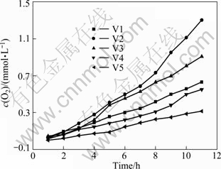
Fig. 12 Dependence of O2 evolution on time of photo reactions for compounded V2O5-TiO2 photocatalysts irradiated by UV-light
Therefore, TiO2 compounded with V2O5 and WO3 in a suitable amount can improve the photocatalytic activity of TiO2. It can be explained by the theory of direct band gap transition and indirect band gap transition.
Different semiconductors have different band structures. Electron transitions happen between the minimum of the conduct band and the maximum of valence band. If the electron keeps the same wave vector k in the same Brillouin zone during the transition, it shows vertical transition in the energy band diagram. This is the so-called vertical transition. As shown in Fig. 13(a) [24], electrons locating on the top of the valence band absorb a certain wavelength of light, then are excited, and transit from position O to O��. Because there are only electrons, holes and photoelectrons in the process of vertical transition, the energy and momentum conservation is a direct, sustained balance among these three quanta. The vertical transition is also named as direct band gap transition or direct transition, and the corresponding semiconductors are called direct gap semiconductors. On the contrary, if electrons don��t keep the wave vector k constant during the transition, its difference is greater than the reciprocal of lattice constant, and then electron transition between their minimum of conduct band and maximum of valence band is non-vertical. So it is called non-vertical transition. As shown in Fig. 13(b), electrons locating on the top of the valence band absorb a certain wavelength of light, then are excited, and transit from position O to O��. Since O�� is not the location of minimum energy in the conduction band, under the role of phonons, electrons continue to transit to the location O���, which is the minimum energy in the conduction band. Compared with the vertical transition, in addition to electrons, holes and photoelectrons, phonons must participate in order to meet the quasi-momentum conservation. So the non-vertical transition is also named as indirect band gap transition or indirect transition, and the corresponding semiconductors are called indirect gap semiconductors. The role of phonons is shown in Fig. 14 [13].
Rutile TiO2 is a direct gap semiconductor. When the surface of the semiconductor is irradiated by the light whose energy is high enough to excite its valence electrons, valence electrons will obtain much energy to jump onto the bottom of conduction band from the top of valence band, and the whole process keeps in the same vertical line. There are only electronics, holes and photoelectrons in entire transition process. It is a direct transition. However, both WO3 and V2O5 are indirect gap semiconductors, and valence electrons locating on the top of the valence band absorb a certain wavelength of light, then are excited, and transit from position O to O��. Under the role of phonons, electrons continue to transit to the location O���, which is the minimum energy in the conduction band. There are electrons, holes and photons, photoelectrons in entire transition process. It is indirect transition. Usually, the probability of indirect transition is much less than that of the direct transition. But for the indirect transition involving phonons, as long as the incident photon energy is equal to or greater than the band gap of semiconductor materials, i.e.![]() ��Eg, then electrons locating in the valence band with the energy difference from its position to the top of valence band within the range of
��Eg, then electrons locating in the valence band with the energy difference from its position to the top of valence band within the range of![]() and electrons locating in the conduction band with the energy different from its position to the bottom of conduction band within the range of
and electrons locating in the conduction band with the energy different from its position to the bottom of conduction band within the range of ![]() can participate in the transition process. So it expands the transition scope, to some extent, it also makes up for the probability in indirect transition. So the total probability of transition is not too small.
can participate in the transition process. So it expands the transition scope, to some extent, it also makes up for the probability in indirect transition. So the total probability of transition is not too small.
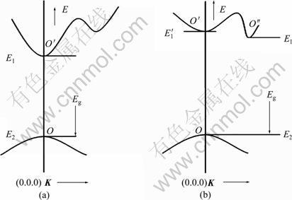
Fig. 13 Sketch of transition of direct and indirect band gap: (a) Transition of direct band gap; (b) Transition of indirect band gap
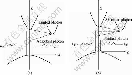
Fig. 14 Transition in indirect band gap: (a) Absorb photon; (b) Emit photon
Rutile TiO2 is a direct gap semiconductor. It is easy for electrons locating in valence band to have a direct transition, and the probability of the combination of photo electrons and holes is large in the direct transition if there is no impurity levels and defect levels. So the separation efficiency of photo electrons and holes is low, which leads to a low photoactivity. After being compounded with V2O5 and WO3, with the minimum of energy level whose conduction band is higher than that of TiO2, driven by the potential difference, photoelectrons can be gathered in conduction band of V2O5 and WO3, respectively. However, both WO3 and V2O5 are indirect gap semiconductors, and both of their minimum of conduct band and maximum of valence band are non-vertical, which means that they are in different wave vector k. It is reported that the theoretical combination probability of direct gap semiconductors is at least 103 times more than that of indirect gap semiconductors under 300 K [24]. So V2O5 and WO3 compounding in a suitable amount can improve the photocatalytic activity of rutile TiO2 obviously. Since the position of the minimum of conduct band of WO3 is lower than that of V2O5, the photoelectrons are easier to gather in the conduction band of WO3 than in that of V2O5, which in turn increases the separation efficiency of photo electrons and holes. Therefore, suitable WO3 compounding can improve the photoactivity of TiO2 more largely than that of V2O5. However, when TiO2 is compounded by WO3 or V2O5 to overdose, holes locating in valence band can hardly be captured by the OH- and the efficiency of O2 evolution is reduced.
4 Conclusions
1) According to the transmitting spectra, by extrapolation method, the band gap of WO3 and V2O5 are about 2.8 eV and 2.14 eV, respectively, and the band gap of rutile TiO2 is about 3.08 eV.
2) The speeds of water splitting for 2%WO3-TiO2 and 8%V2O5-TiO2 photocatalysts are 420 ��mol/(L��h) and 110 ��mol/(L��h), respectively, under UV irradiation.
3) The photoluminescence performance is not a decisive factor for the photoactivities of TiO2 photocatalysts compounded with V2O5 and WO3.
References
[1] OHSAKA T, YAMAOKA S, SHIMOMURA O. Effect of hydrostatic pressure on the Raman spectrum of anatase (TiO2) [J]. Solid State Communications, 1979, 30(6): 345-347.
[2] JOS? M E F, ALEJANDRO M A. Theoretical study of the emission of light stimulated by phonons in indirect bandgap semiconductor [J]. Procedia Computer Science, 2011, 7: 231-232.
[3] JOS? M E F, ALEJANDRO M A, Theoretical Study about the gain in indirect bandgap semiconductor optical cavities [J]. Physica B: Condensed Matter, 2012, 407: 2044-2049.
[4] YIN J L, HU M L, YU Z Z, ZHANG C, SUN L Z, ZHONG J X, Direct or indirect semiconductor: The role of stacking fault in h-BN [J]. Physica B, 2011, 406: 2293-2297.
[5] WANG Ya-chun, YAO Tian-kai, LI Hui, LIAN Jie, LI Ji-hui, LI Zhi-ping, ZHANG Jing-wu, GOU Hui-yang. Structural stability, phase transition, and mechanical and electronic properties of transition metal nitrides MN(M=Tc, Re, Os, and Ir): First-principles calculations [J]. Computational Materials Science, 2012, 56: 116-121.
[6] FARAG A A M, MANSOUR A M, AMMAR A H, RAFEA M A. Characterization of electrical and optical absorption of organic based methyl orange for photovoltaic application [J]. Synthetic Metals, 2011, 161: 2135-2143.
[7] MEILIKHOV E Z, FARZETDINOVA R M. Metal�Cinsulator transition induced by ?uctuations of the magnetic potential in the quantum well of the semiconductor structure with magnetic impurities�� ��-layer [J]. Physics Letters A, 2011, 375: 3731-3738.
[8] TONG Hai-xia, CHEN Qi-yuan, YIN Zhou-lan, HU Hui-ping, LI Jie, ZHAO Li. Preparation and photocatalytic activity of TiO2 photocatalyst coated with WO3 [J]. The Chinese Journal of Nonferrous Metals, 2008, 4(18): 682-687. (in Chinese)
[9] GAO You-liang, CHEN Qi-yuan, TONG Hai-xia, HU Hui-ping, QIAN Dong1, YANG Ya-hui, ZHOU Jian-liang. Preparation of TiO2 photocatalyst loaded with V2O5 for O2 evolution [J]. Journal of Central South University of Technology, 2009, 16: 919-925.
[10] MORRISON S R. Electrochemistry at semiconductor and oxidized metal electrodes [J]. Beijing: Science Press, 1988, 199. (in Chinese)
[11] XU Lian-bo, FAN Yi-ning, LIU Liu, LIN Ming, CHEN Yi. The dispersion state and catalytic performance of vanadium-oxygen species on the surface of V2O5/TiO2 catalyst [J]. Science in China (Series B), 2002, 32(3): 235-242.
[12] HU Rong-rong, ZHONG Shun-he. Mutual modification of V2O5 and TiO2 on the surface of supported coupled-semiconductor V2O5-TiO2/ SiO2 [J]. Chinese Journal of Catalysis, 2005, 16(1): 32-36.
[13] LIU En-ke, ZHU Bing-sheng, LUO Jin-sheng. Semiconductor physics [M]. Beijing: National Defence Industry Press, 1994: 25. (in Chinese)
[14] LETHY K J, BEENA D, VINOD K R, MAHADEVAN P V P, GANESAN V, SATHE V. Structural, optical and morphological studies on laser ablated nanostructured WO3 thin films [J]. Applied Surface Science, 2008, 254: 2369�C2376.
[15] XU Min, QIU Jia-wen, HE De-yan. Microstructures and electrical and optical properties of vanadium pentoxide films [J]. Vacuum Science and Technology, 2003, 25(6): 373-376. (in Chinese)
[16] IKARI H, OKANISHI K, TOMITA M. Fluorescence MDR features of Eu3+ doped sol�Cgel TiO2 hydrate microspheres [J]. Opt Mater, 2008, 30(8): 1323-1326.
[17] WANG Yan-qin, ZHANG Li, CHENG Hu-min, MA Ji-ming. The photocatalytic properties of transition metal ion-doped TiO2 nanoparticles-Photocatalytic degradation of rhodamine B [J]. Chemical Journal of Chinese Universities, 2000, 6(21): 958-960. (in Chinese)
[18] LI Dan-zhen, ZHEN Yi, FU Zhi-xian. Photoluminescence of nano-TiO2 [J]. Chinese Journal of Materials Research, 2000, 14(6): 639-642. (in Chinese)
[19] LI D, OHASHI N, HISHITA S, KOLODIAZHNYI T, HANEDA H. Origin of visible-light-driven photocatalysis: A comparative study on N/F-doped and N-F-codoped TiO2 powders by means of experimental characterizations and theoretical calculations [J]. J Solid State Chem, 2005, 178(11): 3293-3302.
[20] SERPONE N, LAWLESS D, KHAIRUTDINOV R. Size effects on the photophysical properties of colloidal anatase TiO2 Particles: Size quantization or direct transitions in this indirect semiconductor [J]. J Phys Chem, 1995, 99, 16646-16654.
[21] EMELINE A V, SERPONE N. Photo-induced processes in heterogeneous nanosystems from photoexcitation to interfacial chemical transformations [J]. Chem Phys Lett, 2001, 345(54): 105-110.
[22] HUANG De-xiu. Semiconductor optoelectronics [M]. Chengdu: Electronic Science and Technology University Press, 1994: 4. (in Chinese)
[23] JING Li-qiang, XIN Bai-fu, WANG De-jun, YUAN Fu-long. Relationships between photoluminescence performance and photocatalytic activity of ZnO and TiO2 nanoparticles [J]. Chemical Journal of Chinese Universities, 2005, 26(1): 111-115. (in Chinese)
[24] FANG Zhi-lie. Semiconductor luminescent materials and devices [M]. Shanghai: Fudan University Press, 1992: 92. (in Chinese)
(Edited by YANG Bing)
Foundation item: Project(11JJ5010) supported by the Natural Science Foundation of Hunan Province, China; Project(2011RS4069) supported by the Planned Science and Technology Program of Hunan Province, China; Project supported by the Postdoctoral Science Foundation of Central South University, China
Received date: 2011-09-26; Accepted date: 2012-04-16
Corresponding author: TONG Hai-xia, PhD; Tel: +86-731-85258733; E-mail: tonghaixia@126.com
Abstract: The photo absorbing, photo transmitting and photoluminescence performances of TiO2 photocatalysts compounded with V2O5 or WO3 were investigated by UV-Vis spectra, transmitting spectra, and PL spectra, respectively. The energy band structures of TiO2 photocatalysts were analyzed. The photocatalytic activities of the TiO2 photocatalysts were investigated by splitting of water for O2 evolution. The results indicate that the band gaps of WO3 and V2O5 are about 2.8 and 2.14 eV, respectively, and the band gap of rutile TiO2 is about 3.08 eV. Speeds of water splitting for 2%WO3-TiO2 and 8%V2O5-TiO2 photocatalysts are 420 and 110 ��mol/(L��h), respectively, under UV light irradiation. V2O5 and WO3 compounded with suitable concentration can improve the photocatalytic activity of TiO2 with Fe3+ as electron acceptor.
