
J. Cent. South Univ. Technol. (2009) 16: 0621-0628
DOI: 10.1007/s11771-009-0103-6
![]()
Power management unit chip design for automobile active-matrix organic light-emitting diode display module
KIM J H1, PARK J H1, KIM J H1, CAO T V1, LEE T Y1, BAN H J2, YANG K2, KIM H G2, HA P B1, KIM Y H1
(1. Department of Electronic Engineering, Changwon National University, 9 Sarim-Dong,
Changwon 641-773, Korea;
2. Denso PS Electronics Corporation, 47 Seongsan-Dong, Changwon 641-315, Korea)
Abstract:
A power management unit (PMU) chip supplying dual panel supply voltage, which has a low electro-magnetic interference (EMI) characteristic and is favorable for miniaturization, is designed. A two-phase charge pump circuit using external pumping capacitor increases its pumping current and works out the charge-loss problem by using bulk-potential biasing circuit. A low-power start-up circuit is also proposed to reduce the power consumption of the band-gap reference voltage generator. And the ring oscillator used in the ELVSS power circuit is designed with logic devices by supplying the logic power supply to reduce the layout area. The PMU chip is designed with MagnaChip��s 0.25 mm high-voltage process. The driving currents of ELVDD and ELVSS are more than 50 mA when a SPICE simulation is done.
Key words:
DC-DC converter; AMOLED; charge pumping; power management unit (PMU); dual panel supply voltage��
1 Introduction
The flat-panel display (FPD) is used in hand-held devices like PDAs (personal digital assistant), cellular phones, digital cameras and media players, as well as automobile clusters [1]. TFT-LCD (thin film transistor-liquid crystal display) is used widely as automobile clusters. Recently, the OLED (organic light-emitting diode) display has been expanded incessantly. AMOLED (active-matrix OLED) is favorable for making it ultrathin and low-mass with advantages of wide viewing angle, excellent luminance, high power efficiency, and paper-thin thickness [2]. AMOLED display module consists of display panel, display driver IC (integrated circuit), and PMU (power management unit) supplying power supplies for the panel and the display driver IC. The PMU chips are classified into PMU chips with single panel supply voltage and PMU chips with dual panel supply voltage. The PMU chip with single panel supply voltage of 10 V has been already developed [3]. And the research on the PMU chip with dual panel supply voltage is going on nowadays.
VBP (9-16 V) and VCC (5 V) are used as input voltages, and ELVDD (5 V) and ELVSS (-6 V) are used as panel driving voltages. VCI (2.8 V) is used for the supply voltage of driver IC, and VDDI (1.8 V) is used for the interface as output voltages. There are four voltage regulators for VCI, VDDI, VLP (2.8 V), and ELVDD that generate internal supply voltages used in the chip from VBP of 9 to 16 V. VLP is used for a supply voltage to the level detector and the ring oscillator and ELVDD for a supply voltage to the AMOLED panel. And the reference bias generator generates reference voltages for VLP, ELVDD, ELVSS, VCI, and VDDI. Signals such as REF_ON, VLP_ON, ELVDD_ON, ELVSS_ON, VCI_ON, and VDDI_ON are used for turning on sequentially the reference bias generator, the voltage regulators, and the ELVSS generator. ELVDD of 5 V can be generated either by linearly-regulating the VBP voltage [4-5] or by using a buck converter [6-8] that is a type of switching regulator. On the other hand, ELVSS can be generated either by using a buck-boost converter supplying a negative voltage [9] or by using a DC-DC converter of charge-pumping type. Switching regulators of PWM (pulse width modulation) type using inductors are vulnerable to EMI (electro-magnetic interference) radiation and noise, and realize the limitations in miniaturization due to the use of discrete devices including the inductors. And many researches on the DC-DC converter of pumping type have been done for mobile devices using a battery voltage of 3.7 V [10-11]. For an automobile cluster with a battery voltage of 12 V, just a research on a positive charge pump boosting VDD of 10 V has been done. There is, however, no research on a PMU chip supplying dual panel supply voltage including a negative voltage of -6 V, and being designed as one chip.
A PMU chip supplying ELVDD, ELVSS, VCI, and VDDI for an 8.382 cm AMOLED panel used as an automobile cluster is designed as one chip to minimize
the power module of the cluster. A two-phase charge pump circuit using external pumping capacitor is proposed to increase its pumping current. A body-potential bias circuit [12] is used to eliminate the charge-loss problem springing up in pumping [13], and a simplified control clock switching between 0 V and VPP is used in the proposed charge pump circuit. A low- power start-up circuit used in the band-gap reference (BGR) voltage generator is proposed. A method with the logic power voltage VLP is used in the ELVSS power circuit to reduce the layout size of the ring oscillator. A PMU chip supplying dual panel power voltage is designed with MagnaChip��s 0.25 mm high-voltage process.
2 Circuit design
The designed PMU chip consists of reference bias generator and voltage regulator that supplies voltages VPP, VCI, ELVDD, VLP, and VDDI, and DC-DC converter that supplies voltage ELVSS, as shown in Fig.1. VBP and VCC are used as input voltages, and ELVDD, ELVSS, VCI, and VDDI are used as output voltages. There are four voltage regulators of VCI, VDDI, VLP, and ELVDD, which generate internal supply voltages used in the chip from VBP of 9 to 16 V. VLP is used as the supply voltage for the level detector and the ring oscillator in the ELVSS power circuit. And the reference bias generator generates reference voltages for VLP, ELVDD, ELVSS, VCI, and VDDI. Signals such as REF_ON, VLP_ON, ELVDD_ON, ELVSS_ON, VCI_ON, and VDDI_ON are used for turning on sequentially the reference bias generator, the voltage regulators, and the ELVSS generator.
Driving voltage ELVSS of an 8.382 cm AMOLED display panel requires a driving voltage of -6 V and a maximum driving current of over 50 mA. Fig.2 shows a
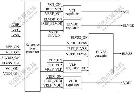
Fig.1 Block diagram of PMU chip
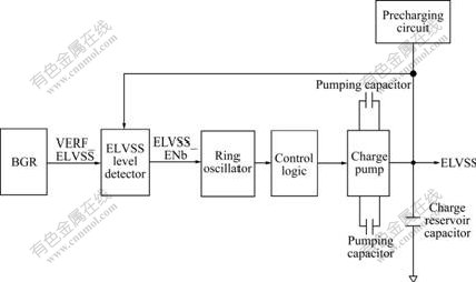
Fig.2 Simplified block diagram of DC-DC converter of charge pump type
DC-DC converter meeting the requirement, which consists of the BGR voltage generator, the ELVSS level detector, the ring oscillator, the control clock logic, the precharge circuit, and the single-stage charge pump. It is operated so that the output voltage ELVSS reaches the target value by using the negative feedback mechanism.
Charge pumps with an external pumping capacitor are usually based on H-tree charge pumps [14], as shown in Fig.3. Conventional negative charge pump circuit consists of external pumping capacitor CP of 1 ��F, charge reservoir capacitor CR, NMOS (N-channel metal oxide semiconductor) transistor MN1 that precharges node N1 to GND (ground), inverter INV that makes node N2 of the pumping capacitor switch between GND and VIN, and charge transfer switch MN2 that transfers negative charge to VOUT when node N2 switches from VBP to GND and voltage of node N1 becomes -VBP by capacitive coupling of capacitor CP. When CLK0 is VBP,
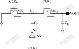
Fig.3 Conventional H-tree negative charge pump circuit
precharging transistor MN1 turns on, and voltage of node N1 precharges to GND. After this, voltage of node N1 precharges to GND. After this, CLK0 switches from VBP to VOUT and so MN1 turns off. After this, CLK1 switches from VOUT to VBP and voltage of node N2 switches from VBP to GND, so voltage of node N1 becomes -VBP from GND. Then, transistor MN2 turns on and negative charge of transistor N1 is transferred to node VOUT.
In case of the conventional charge pump circuit, the charge-loss problem that part of pumped charge drains off to deep N-well occurs since NPN BJT (bipolar junction transistor) parasitic to transistor MN2 is in the active region when voltage of node N1 switches from GND to -VBP. And CLK0 and CLK1 that turn on/off transistors MN1 and MN2 are clock signals switching between VBP and VOUT (=ELVSS). MN1 and MN2 securely turn off when the levels of these clocks are VOUT.
The proposed ELVSS charge pump circuit uses four clock signals shown in Fig.4 and consists of precharge control circuit (MP1, MN1, MN2, MP2, MN3 and MN4) to precharge node N1 to GND, cross-coupled NMOS charge transfer switches (MN5 and MN6), body potential biasing circuit, external pumping capacitors (C1 and C2), and external charge reservoir capacitor CR. The timing diagram of the ELVSS charge pump in the steady state is shown in Fig.5. At t4 when CLK0 is 0 V, voltage of node G2 becomes VBP, MN1 turns on and voltage of node ND1 precharges to 0 V for the circuit consisting of MP1, MN1,
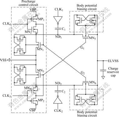
Fig.4 Proposed two-phase ELVSS charge pump circuit
and MN2 of the precharge control circuit. When CLK1 switches from 0 V to VBP, voltages of nodes ND1 and G2 are all -VBP by capacitive coupling of C1. At t0 when CLK3 is 0 V, voltage of node G1 becomes VBP, MN3 turns on, and voltage of node ND2 precharges to 0 V. When CLK3 is VBP, voltages of nodes ND2 and G1 become -VBP by capacitive coupling of C2 with MN4 turned on, as shown in Fig.5. When voltages of nodes ND1 and ND2 switch to -VBP and 0 V by capacitive coupling of C1 and C2, respectively, MN5 turns on and MN6 turns off. Thus, negative charge transfers to node ELVSS through MN5. When voltages of nodes ND2 and ND1 switch to -VBP and 0 V, respectively, MN6 turns on and MN5 turns off. Thus, negative charge of node N2 transfers to node ELVSS through MN6, and negative charge pumping occurs twice per cycle, as shown in Fig.5. And the pumping current of ELVSS charge pump is increased by proposing a two-phase charge pump of Fig.4 instead of a single-phase charge pump of Fig.3.
Fig.6 shows the BGR voltage generator circuit. As
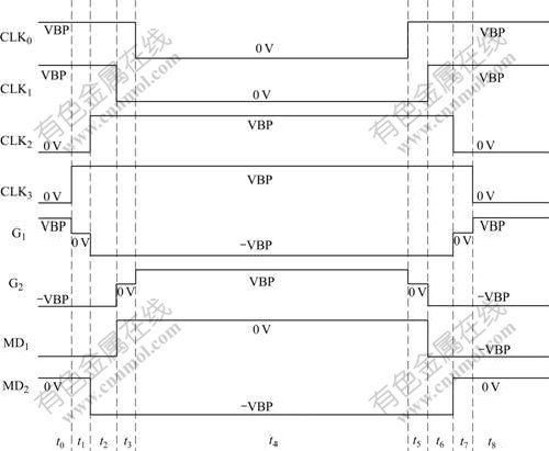
Fig.5 Timing diagram of ELVSS charge pump in steady state
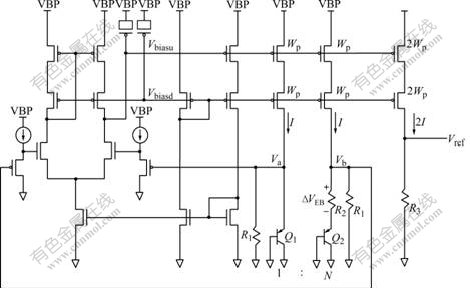
Fig.6 Band-gap reference (BGR) voltage generator circuit
can be seen in Eqn.(1), reference current Iref (=2I) consists of two terms. One term with VT (thermal voltage) increases with the increase of temperature and the other term with VEB (emitter-base voltage) decreases with the increase of temperature. Thus, the reference current is insensitive to PVT variations [15] and the reference voltage Vref on R3 is also insensitive to PVT (process voltage temperature) variations.
![]() (1)
(1)
![]() (2)
(2)
where N (=10) is the ratio of area of PNP BJT emitter Q1 to that of Q2.
As can be seen in Fig.7, voltage of node N1 is VBP-2(|VTP|+|VDSAT|) in the conventional start-up circuit. Since voltage of node N1 increases with the increase of the battery supply voltage VBP, current flowing through MN3 also increases. And the current flowing through MP3 also increases since the voltage difference between the source and the gate increases. New start-up circuit of Fig.8 is proposed to enhance this kind of current increase at high-voltage VBP. In case of the proposed start-up circuit, the current flowing through MN3 decreases since the drain node voltage of MN3 decreases by inserting N PMOS (P-channel metal oxide semiconductor) diodes between node N1 and drain node of MN3. And the current flowing through MP3 decreases since the current flowing through MN3 decreases, and |VDSAT| decreases. So the voltage difference between the source and the gate of MP3 decreases.
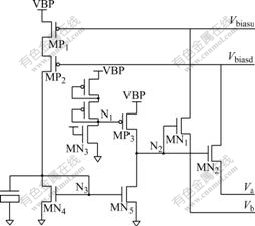
Fig.7 Conventional start-up circuit
Fig.9 shows a proposed ELVSS level detector outputting OSC_ENb of 0 V that enables the ring oscillator of Fig.2 and the negative charge pumps if |ELVSS/3| is lower than VREF_ELVSS. Thus, voltage ELVSS falls in the negative direction. The ELVSS level detector uses logic supply voltage VLP and PMOS differential pair of the comparator uses logic transistors. Reliability of the logic devices used in the comparator is secured by discharging node N1 to 0 V with signals ELVSS_EN and ELVSS_ENb in entering stand-by mode.
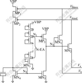
Fig.8 Proposed start-up circuit
The ring oscillator either oscillates if the ELVSS_ENb signal from the level detector of Fig.9 is 0 V or stops if the ELVSS_ENb signal from the level detector of Fig.9 is VLP. If voltage VBP is used as the supply voltage to the ring oscillator, the ring oscillator should be designed with high-voltage devices and its layout area should be increased to meet a long oscillation period of 100 ms. Fig.10 shows a proposed ring oscillator of which layout area is decreased since it is designed with logic devices by supplying the logic power supply VLP to the ring oscillator. Fig.10 shows a VLP-to-VBP level translator of which the purpose is to translate the switching voltage VLP, that is, output signal OSC_ELVSS from the ring oscillator to VBP.
Fig.11 shows the voltage regulator circuit that supplies logic supply voltage VLP of the proposed DC-DC converter. VBP is used as input voltage of the charge pump, driving voltage ELVDD of the AMOLED panel, input voltage VCI of the OLED display driver IC, and voltage VDDI of the interface. Voltage regulator circuit regulates in the steady state such that Vref is equal to Vreg/(N+1). Therefore, Vreg becomes (1+N)Vref.
3 Simulation results
Fig.12 shows the simulation results of on-current of the BGR circuit with respect to battery power supply VBP when simulation is performed under the condition

Fig.9 Proposed ELVSS level detector circuit
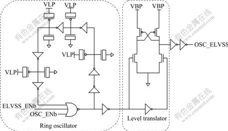
Fig.10 Proposed ring oscillator circuit
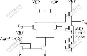
Fig.11 Proposed voltage regulator circuit
of fast transistor model and temperature of -40 ��. This shows that the on-current of the proposed BGR is 42% lower than that of the conventional counterpart.
Fig.13 shows the simulation results of pumping current with respect to the oscillation period for the designed ELVSS charge pump when SPICE simulation is
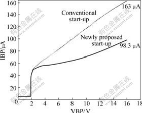
Fig.12 On-current IBP vs VBP of BGR
done under the condition of slow transistor model, VBP=9 V and temperature of 90 ��. As shown in Fig.13, the pumping current IELVSS of the ELVSS charge pump is 52.11 mA at the oscillation period of 100 ms as a simula-
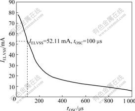
Fig.13 Pumping current of designed ELVSS charge pump with respect to oscillation period
tion result, which almost approaches 60 mA that is IELVSS under the ideal condition and is larger than the loading current of 50 mA at the panel. The capacitances of the external pumping capacitors C1 and C2 of the ELVSS charge pump in Fig.4 are 1 mF. The oscillation period of the ring oscillator is designed to be 100 ms. IELVSS under the ideal condition is calculated according to Eqn.(3) and the pumping current of the two-phase charge pumping scheme is twice larger than that of the single-phase counterpart.
![]() ��2=
��2=![]() ��2=60 mA (3)
��2=60 mA (3)
where Cp is the capacitance of the external pumping capacitors C1 and C2, here it equals 1 ��F.
Fig.14 shows simulation results of power-on
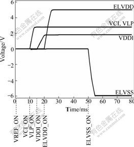
Fig.14 Output voltage sequence of designed DC-DC converter
sequence for the designed DC-DC converter when simulation is done under the condition of slow transistor model, VBP=9 V and temperature of 90 ��.
A PMU chip supplying dual panel supply voltage for an 8.382 cm AMOLED display module is designed with MagnaChip��s 0.25 mm high-voltage process. The layout area is 460 mm ��840 mm.
4 Conclusions
(1) A PMU chip supplying dual panel supply voltage for an 8.382 cm OLED display module is designed with MagnaChip��s 0.25 mm high-voltage process. The designed PMU chip supplies ELVDD, ELVSS, VCI, and VDDI.
(2) The designed two-phase charge pump circuit using external charge pumping capacitor can drive a current of more than 50 mA required for the AMOLED panel.
(3) The power consumption of the start-up circuit is 42% smaller since a low-power technique is applied to the start-up circuit of the band-gap reference voltage generator.
(4) The layout size is reduced since logic supply voltage is used for the ring oscillator instead of the battery power supply. The layout size of the designed PMU chip is 477 mm��653 mm.
(5) The PMU chip with dual panel supply voltage is the best solution for the AMOLED display module requiring both low EMI characteristic and miniaturization.
References
[1] KIMURA N, FURUICHI S. Development of organic light emitting diode (OLED) driver for automotive component [J]. Oki Technical Review, 2007, 74(3): 10-13.
[2] UCHIKOGA S. Future trend of flat panel displays and comparison of its driving methods [C]// Proceedings of IEEE International Symposium on Power Semiconductor Devices and IC��s. Naples, 2006: 1-5.
[3] LEE T Y, PARK J H, KIM J H, KIM T H, CAO T V, KIM J H, BAN H J, YANG K, KIM H G, HA P B, KIM Y H. A DC-DC converter design for OLED display module [J]. The Korean Institute of Maritime Information and Communication Sciences, 2008, 12(3): 518-526.
[4] HORIGUCHI M, AOKI M, ETOH J, TANAKA H, IKENAGA S, ITOH K, KAJIGAYA K, KOTANI H, OHSHIMA K, MATSUMOTO T. A tunable CMOS DRAM voltage limiter with stabilized feedback amplifier [J]. IEEE Journal of Solid-State Circuits, 1990, 25(10): 1129-1135.
[5] JOU S J, CHEN T L. On-chip voltage down converter for low-power digital system [J]. IEEE Transactions on Circuits and System II: Analog and Digital Signal Processing, 1998, 45(5): 617-625.
[6] STRATAKOS A J, SANDERS S R, BRODERSEN R W. High-efficiency low-voltage DC-DC conversion for portable applications [C]// Proceedings of International Workshop on Low Power Design. Napa Valley, California, 1994: 105-110.
[7] JUNG S H, JUNG N S, HWANG J T, CHO G H. An integrated CMOS DC-DC converter for battery-operated systems [C]// Proceedings of IEEE Power Electronics Specialists Conference. Lausanne, 1999: 43-47.
[8] XIAO J W, PETERCHEV A, ZHANG J H, SANDERS S. An ultra-low-power digitally controlled buck converter IC for cellular phone applications [C]// Proceedings of Applied Power Electronics Conference and Exposition. Anaheim, California, 2004: 383-391.
[9] ZHAO Ling-yin, QIAN Jin-rong. DC-DC power conversions and system design considerations for battery operated system [R]. Texas Instruments, USA. 2006.
[10] YING T R, KI W H, CHAN M S. Area-efficient CMOS charge pumps for LCD drivers[J]. IEEE Journal of Solid-State Circuits, 2003, 38(10): 1721-1725.
[11] LIM G H, SONG S Y, PARK J H, LEE L Z, LEE C H, LEE T Y, CHO G S, PARK M H, HA P B, KIM Y H. Charge pump design for TFT-LCD driver IC using stack MIM capacitor [J]. IEICE Transactions on Electronics, 2008, 91(6): 928-935.
[12] CHO S I, HEO J S, MIN K S, KIM Y H. A boosted voltage generator for low-voltage DRAMs [J]. Current Applied Physics, 2003, 3(6): 501-505.
[13] FAVRAT P, DEVAL P, DECLERCQ M J. A high-efficiency CMOS voltage doubler [J]. IEEE Journal of Solid-State Circuits, 1998, 33(3): 410-416.
[14] BAYER E, SCHMELLER H. A high efficiency single-cell cascaded charge pump topology [C]// Proceedings of IEEE Power Electronics Specialists Conference. Vancouver, 2001: 290-295.
[15] CHO S I, JEONG H G, SHIN H G, KIM Y H. A CMOS bandgap reference voltage generator with reduced voltage variation and BJT area [J]. Current Applied Physics, 2007, 7(1): 92-95.
(Edited by CHEN Wei-ping)
Received date: 2008-10-20; Accepted date: 2009-03-02
Corresponding author: KIM Y H, Professor, PhD; Tel: +82-55-285-1023; E-mail: youngkim@changwon.ac.kr
