
Microstructure of ternary Zn1-xCdxO films on silicon substrate
LU Huan-ming(¬����), YE Zhi-zhen(Ҷ־��), MA De-wei(����ΰ), HUANG Jing-yun(�ƾ���),
ZHU Li-ping(����Ƽ), ZHAO Bing-hui(�Ա���)
(State Key Laboratory of Silicon Materials, Zhejiang University, Hangzhou 310027, China)
Abstract:
Ternary Zn1-xCdxO alloying films were deposited on silicon substrates by a reactive magnetron sputtering method. The structures of the films were characterized by transmission electron microscopy(TEM) and X-ray diffraction(XRD) analysis, respectively. The XRD measurement shows that the wurtzite-type structure of Zn1-xCdxO can be stabilized up to Cd content of x=0.53 without a cubic CdO phase separation. The TEM measurement shows that the films have a columnar structure and the grains are highly c-axis oriented perpendicularly on silicon substrate although some grain boundaries are slightly tilted. High resolution TEM observation indicates that a native layer of amorphous SiO2 exists at the ZnCdO/Si interface and that ZnCdO grains with c-axis preferred orientation nucleate directly on substrate surface.
Key words:
ZnCdO; microstructure; sputtering CLC number: TG304;
Document code: A
1 INTRODUCTION
Wide and direct band gap semiconductors have gained substantial attentions due to their potential applications in short wavelength optoelectronic devices[1-4]. ZnO is a ��-�� semiconductor of a hexagonal wurtzite-type structure and exhibits attractive properties with a direct band-gap of 3.3eV and a large excitonic binding energy of 60meV. Therefore, ZnO is considered as an important luminescent material. Furthermore, the band-gap of ZnO can be modulated by means of alloying with CdO to widen the useable wavelength range[5-8]. CdO has a cubic structure with a narrower direct band-gap of 2.3eV. Therefore, the luminescence of ZnCdO alloys can cover green, blue to ultraviolet light spectra.
Several techniques were attempted to deposit ZnCdO alloying films, such as sol-gel[6], spray pyrolysis[7, 8], molecular beam epitaxy[9] and pulsed laser deposition methods[2, 10]. However, the crystalline quality of reported ZnCdO alloying was not satisfying due to the fine crystalline without preferred orientation. Since the optical and electrical properties in the device applications essentially depend on the quality of the films, detailed knowledge of the microstructure of ZnCdO film is required for improvement in crystal quality and for device applications.
We have successfully deposited ternary Zn1-x- CdxO(0��x��0.53) alloy films by reactive magnetron sputtering method[11]. In this paper, we focus on the microstructure of ZnCdO films on silicon substrates.
2 EXPERIMENTAL
Ternary Zn1-xCdxO(0��x��0.53) alloying films have been prepared by reactive magnetron sputtering method on Si(111) in argon and oxygen mixture gas. Zinc-cadmium metals with varied ratios were used as sputtering targets. The sputtering current and sputtering voltage were 0.2A and 200V, respectively. The specific flux of argon and oxygen was controlled at a ratio of Ar to O2 of 1��4, and the total pressure were maintained at 4.0Pa. The substrate temperature was 450��. The deposition time was 30min for each sample. Details of the growth processing have been described elsewhere[12, 13].
The crystal structures of the samples were investigated by X-ray diffraction(XRD), where a CuK��(��=0.154056nm) source was used. Microscopic characterizations were performed by transmission electron microscopy(TEM) in cross-section and plan-view geometry using a PHILIPS CM200 microscope operated at 200kV. TEM specimens were prepared by standard ion-beam thinning procedures with a precision ion polishing system at an ion acceleration energy of 4keV. For plan-view observations, the silicon substrate was milled by Ar ions mainly from the backside and then the top surface of ZnCdO was slightly milled so that the observed ZnCdO region of TEM sample was near interface.
3 RESULTS AND DISCUSSION
The XRD patterns of Zn1-xCdxO(0��x��1.0) films are shown in Fig.1. For x��0.53,the film exhibits only (002) Bragg peaks from hexagonal wurtzite ZnCdO without CdO phase, which indicates that wurtzite structure of the grown films is stabilized and that the ZnCdO films are of nearly complete c-axis orientations. For further increasing the Cd content up to x=0.77, the film shows two Bragg peaks. One is the (002) reflection from hexagonal wurtzite ZnCdO phase and the other is the (200) reflection from cubic CdO phase. Due to the coexistence of hexagonal ZnCdO and cubic CdO, the intensities of the Bragg peaks decrease greatly with broadening full width at half maximum (FWHM), which suggests that the crystallinity is reduced dramatically for film with the Cd content of x=0.77. For the pure CdO film, only the (200) peak is observed. For the samples with x=0 to x=0.77, the corresponding lattice parameters c calculated from the (002) peaks are 5.229�@, 5.235�@, 5.244�@, 5.247�@ and 5.253�@, respectively. The lattice parameters increase when Cd content increases in hexagonal wurtzite structure. It is contributed to that smaller Zn(with ionic radius of 0.74�@) is substituted by larger Cd(with ionic radius of 0.97�@).
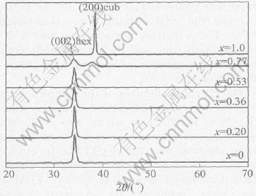
Fig.1 XRD patterns of Zn1-xCdxO(0��x��1.0) films deposited on Si(111) substrates at 450��
Typical bright-field TEM image in plan-view geometry from ZnCdO samples on silicon substrate, shown in Fig.2(a), indicates that the diameter of grains is about 100nm in lateral dimension. Fig.2(b) shows its corresponding SAD pattern. The diffraction spots of Si[111] zone axis and diffraction rings of ZnCdO, {100}, {110}, {200}, {210} and {300} planes etc, which all belong to [001] zone axis of ZnCdO, are observed. But other low index planes of ZnCdO, such as {002}, {101}, {102}, {103} and {112}, are absent, suggesting that all grains of film have a preferred c-axis orientation perpendicular to substrate surface. This is in agreement with the results of XRD pattern.
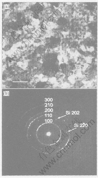
Fig.2 Plan-view bright-field TEM image(a) and corresponding SAD pattern(b) of ZnCdO film on Si(111)
Fig.3 shows a plan-view high-resolution trans-mission electron microscopy(HRTEM) image of ZnCdO film. It shows that three grains, A, B and C, are all in a projection near [001] orientation and rotate each other around c-axis. The Moire fringe between grains indicates that adjacent grains are overlapped, so that some boundaries are slightly tilted although the grains are all c-axis oriented.
Fig.4 shows the cross-section bright field TEM image observed along the [110] zone axis of silicon substrate. It shows that the film is columnar structure. The cross-section HRTEM micrograph, shown in Fig.5, reveals an about 5nm thick amorphous SiO2 interface layer which is a random pattern typical for the amorphous phase. It also indicates that gains with c-axis preferred ori- entation nucleate directly on substrate surface and there is no small crystallite layer of other orientation near interface. Therefore, a highly c-axis orientation is generated from the initial stage of growth. However, some planar defects are observed in as-deposited film in Fig.5.

Fig.3 Plan-view HRTEM image around grain boundary taken in projection near [001] zone axis of ZnCdO
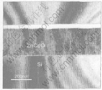
Fig.4 Cross-section bright-field TEM image taken in projection near [110] axis of silicon substrate

Fig.5 Cross-section HRTEM image taken in projection near [110] axis of silicon substrate
In general, ZnO textured film can be grown by an evolution of competition process of the statistically oriented grains. In some depositing condition, small crystallites layer of ZnO with random orientation grows at the beginning on substrate[14]. It can be expected that [001] orientation of ZnO is the fastest crystal growth direction since (001) plane is densest. Therefore only c-axis oriented grains can survive while other grains will be suppressed. Then c-axis oriented grains become dominant at top region of films. As a result, a small crystallites region is formed before columnar grains grow, which is not of good quality.
But in our work, all initial grains of films are c-axis oriented and there is no layer of small crystallites with random orientation and the films are of good quality. The c-axis oriented ZnO film formation from the initial stage of growth can be analyzed from the surface energy minimization considerations. The ZnO has a wurtzite structure and the (001) plane of ZnO has the lowest surface energy[15]. According to the Wulff theorem, the (001) plane will try to grow parallelly to the silicon surface at thermodynamic equilibrium[16]. Therefore only grains with c-axis preferred orientation can nucleate on substrate surface. However, the ZnO film with completely c-axis preferred orientation is formed at the initial stage only if the deposition condition is in optimum range of thermodynamic equilibrium.
The crystal quality of ZnO films with a small crystallites layer is deteriorated and the inhomogeneities in small crystallites layer can strongly affect the heterojunction properties[14]. Therefore, it is important to prepare ZnO films with good crystalline quality that the process parameters during depositing are adjusted in optimum range to achieve the thermodynamic equilibrium condition, so that only c-axis oriented ZnO films grow directly on silicon surface to prevent the formation of small crystallite region. As a result, the better crystalline quality with completely c-axis preferred orientation can be expected.
4 SUMMARY
In summary, ZnCdO films have been prepared on silicon substrates by a reactive magnetron sputtering method. The films have a columnar structure and the grains are highly c-axis oriented. The grains with c-axis preferred orientation nucleate directly on substrate surface due to the minimization of the surface energy and the crystalline quality of film is of good quality. The results show that it is important to control the process parameters in optimum range to avoid small crystallite layer in order to deposit films of high quality.
REFERENCES
[1]Huang M H, Mao S, Feick H, et al. Room-temperature ultraviolet nanowire nanolasers [J]. Science, 2001, 292: 1897-1899.
[2]Misra P, Bhattacharya P, Mallik K, et al. Variation of bandgap with oxygen ambient pressure in MgxZn1-xO thin films grown by pulsed laser deposition [J]. Solid State Commun, 2001, 117: 673-677.
[3]Gao X P, Wang Z L. Nanopropeller arrays of zinc oxide [J]. Appl Phys Lett, 2004, 84: 2883-2885.
[4]CHEN Jian-xun, HUANG Bai-yun, ZHAO Rui-rong, et al. Preparation of ZnO crystal by sol-gel method [J]. Trans Nonferrous Met Soc China, 2001, 11(1): 154-156.
[5]Lee S Y, Li Y, Lee J S, et al. Effects of chemical composition on the optical properties of Zn1-xCdxO thin films [J]. Appl Phys Lett, 2004, 85: 218-220.
[6]Choi Y S, Lee C G, Cho S M. Transparent conducting Zn1-xCdxO thin films prepared by the sol-gel process [J]. Thin Solid Films, 1996, 289: 153-158.
[7]Tabet-Derraz H, Benramdance N, Nacer D, et al. Investigations on Zn1-xCdxO thin films obtained by spray pyrolysis [J]. Solar Energy Materials & Solar Cells, 2002, 73: 249-253.
[8]Vigil O, Vaillant L, F Cruz, et al. Spray pyrolysis deposition of cadmium-zinc oxide thin films [J]. Thin Solid Films, 2000, 361-362: 53-55.
[9]Sakurai K, Takagi T, Kubo T, et al. Spatial composition fluctuations in blue-luminescent ZnCdO semiconductor films grown by molecular beam epitaxy [J]. J Cryst Growth, 2002, 237-239: 514-517.
[10]Makino T, Segawa Y, Kawasaki M, et al. Band gap engineering based on MgxZn1-xO and CdyZn1-yO ternary alloy films [J]. Appl Phys Lett, 2001, 78: 1237-1239.
[11]MA De-wei, Ye Zhi-zhen, HUANG Jing-yun, et al. Structural and optical characterization of Zn1-x CdxO thin films deposited by dc reactive magnetron sputtering [J]. Chin Phys Lett, 2003, 20: 942-943.
[12]MA De-wei, Ye Zhi-zhen, HUANG Jing-yun, et al. Study on Zn1-xCdxO thin films prepared by DC reactive magnetron sputtering [J]. Chinese Journal of Semiconductor, 2003, 24(10): 1053-1056. (in Chinese)
[13]MA D W, YE Z Z, LU H M, et al. Sputtering deposited ternary Zn1-xCdxO crystal films on Si(111) substrates [J]. Thin Solid Films, 2004, 461: 250-255.
[14]Sieber I, Wanderka N, Urban I, et al. Electron microscopic characterization of reactively sputtered ZnO films with different Al-doping levels [J]. Thin Solid Films, 1998, 330: 108-113.
[15]Fujimura N, Nishihara T, Goto S, et al. Control of preferred orientation for ZnOx films: control of self-texture [J]. J Cryst Growth, 1993, 130: 269-279.
[16]Jiang X, Jia C L, Szyszka B. Manufacture of specific structure of aluminum-doped zinc oxide films by patterning the substrate surface [J]. Appl Phys Lett, 2002, 80: 3090-3092.
Foundation item: Project(G2000068306) supported by the National Basic Research Program of China; Project(00085) supported by Test and Analysis Foundation of Zhejiang Province
Received date: 2004-07-11; Accepted date: 2004-11-10
Correspondence: YE Zhi-zhen, Professor, PhD; Tel: +86-571-87952625; E-mail: yezz@zju.edu.cn
