

9R structure in drawn industrial single crystal copper wires
CHEN Jian(�� ��)1, 2, YAN Wen(�� ��)1, 2, FAN Xin-hui(���»�)2
1. School of Materials Science and Chemical Engineering, Xi��an Technological University, Xi��an 710032, China;
2. Department of Applied Physics, Northwestern Polytechical University, Xi��an 710072, China
Received 25 March 2008; accepted 16 September 2008
Abstract:
By using transmission electron microscopy, the microstructures of drawn industrial single crystal copper wires produced by Ohno Continuous Casting(OCC) process were analyzed. The results show that the typical microstructures in the wires mainly include extended planar dislocation boundaries, a small fraction of twins and some dislocation cells sharing boundaries parallel to drawn direction. Besides the typical microstructures, 9R structure configurations were observed in the wires. The formation of 9R polytypes may be caused by the coupled emission of Shockley dislocations from a boundary.
Key words:
industrial single crystal copper wires; 9R structure; cold drawing;
1 Introduction
By use of Ohno Continuous Casting(OCC)[1] process, it is possible to obtain the long and thin industrial single crystal copper wires. Since there is almost no grain boundary (GB) in the copper wires, the quality of electronic signal transmission will be excellent [2-6]. For example, the resistivity of industrial single crystal copper wires is about 15.57% lower than that of ploycrystal wires[4]. Thus, the single crystal copper wires produced by OCC have become very attractive. Up to now, technological parameters for preparing single crystal copper wires by OCC have been identified[5]. However, since the diameter of such wires is too large for some commercial copper cables, they have to be heavily cold drawn to very fine wires. Cold-drawing process makes the microstructures heavily deformed, thus affecting the properties of the wires. For a satisfactory explanation of properties of drawn single crystal copper wires produced by OCC process, it is necessary to systematically investigate the deformation microstructures.
It is commonly accepted that Cu maintains its face centered cubic (FCC) crystal structure. However, specific internal constraints imposed on the Cu crystal may induce polytypic forms. In <110> tilt boundaries slabs of a rhombohedral structure of ��-Sm-type have been found in Cu[7-8]. The ��-Sm-type structure can be derived from FCC structure by a particular stacking of close-packed planes and it can be considered as a Cu polytype. Also, the occurrence of thin atomic layers in copper exhibiting a body-centered cubic(BCC) crystal structure has been theoretically predicted and then found in <211> tilt boundaries of Cu bicrystals[8-9]. Although the occurrence of polytypes is well known in FCC crystals [7-13], the occurrence of polytypes in drawn single crystal copper wires has not been reported yet. In the present work, the microstructures of drawn single crystal copper wires are studied by use of transmission electron microscopy(TEM). Besides the typical microstructures, such as extended planar dislocation boundaries, twins and dislocation cells, the occurrence of 9R polytypes has been found, which can shed a new light on the deformation mechanism of industrial single crystal copper wires drawn at room temperature.
2 Experimental
Single crystal copper wires with 8 mm in diameter were produced by OCC technique. The wires were drawn at room temperature to different diameters. The drawing directions were kept the same in every time of drawing to exclude the influence of drawing direction on deformation microstructure. The true strain of drawn single crystal copper wires is calculated by the following equation:
��=ln(A0/A)=2ln(d0/d) (1)
where �� indicates the true strain of drawn single crystal copper wires. A0 and d0 denote the initial cross-section area and diameter respectively. A and d are those of the drawn single crystal copper wires.
In order to analyze the crystal defects by TEM, the thin foils have been cut from the longitudinal section of the drawn single crystal copper wires. The samples were electropolished in a solution of 500 mL distilled water, 250 mL HPO3, 250 mL ethanol, 50 mL propanal and 5 g carbamide at 4 V and -15 �� using standard methods. TEM observations have been carried out in a JEM-2010 or a Tecnai 20 with acceleration voltage of 200 kV. The drawn direction of the wires was made coincident with the longitudinal axis of the double-tilt specimen holder during the microstructure analysis.
3 Results
Fig.1(a) shows the optical microstructure of the wires produced by OCC process. From Fig.1(a), it can be seen that there are still very few GBs in the wires, but the number of GBs in the wires is much less than that of common copper wires. Then, the copper wires produced by OCC process can be considered as the industrial single crystal copper wires. In some other literatures [3-4], such kind of copper wires are also considered as the single crystal copper wires. Although there are still few grain boundaries, the axial direction of grains in the wires is almost along <100>[3]. Fig.1(b) shows the optical microstructure of drawn wires with a true strain of 0.94, indicating that besides few GBs in the wires, deformation bands resulting from grain subdivision can be observed.
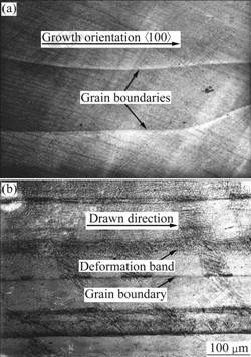
Fig.1 Optical microstructures of single crystal copper wires produced by OCC method: (a) Without deformation; (b) With true strain of 0.94
Fig.2 shows the typical microstructures of deformed industrial single crystal copper wires under TEM observation. Fig.2(b) shows the microstructure of regions denoted by the letter ��A�� in Fig.2(a). From Fig.2, it can be seen that there are three kinds of typical microstructure: 1) a large number of extended planar dislocation boundaries, not parallel to the drawn direction, as shown in Fig.2(a); 2) a small fraction of twins, as shown in Fig.2(b); and 3) some dislocation cells and some boundaries parallel to drawn direction shared by some dislocation cells, as shown in Fig.2(c).
Besides these three kinds of typical microstructures mentioned above, other unexpected structural configurations are also observed in the drawn industrial single crystal copper wires. Fig.3 shows the unexpected structural configurations with the corresponding selected area diffraction pattern and a dark-field image taken from the bright spot arrowed in Fig.3(c). From Figs.3(a) and 3(b), the unexpected microstructures consist of some extremely thin (about 10 nm) plates. The diffraction pattern (Fig.3(c)) is obtained from regions with thin plates and these thin plates can be discerned only when a given plate is in exact Bragg position. For other positions the plates are invisible. Those configurations are likely the deformation twin or stacking fault. However, deformation twin or stacking fault should not change crystal structure and the diffraction pattern in Fig.3(c) definitely does not correspond to that of FCC crystal structure, indicating that there is a polytype phenomenon. According to the indexing result of the diffraction pattern in Fig.3(c), the regions with thin plates are of 9R crystal structure, which is exactly the same as the results reported by DYMEK et al[13].
4 Discussion
4.1 Formation of typical microstructures
In the present work, three kinds of typical microstructures, twins, extended planar dislocation boundaries not parallel to drawn direction and a large number of dislocation cells sharing boundaries parallel to the drawn direction, are found, as shown in Fig.2. Regarding the small fraction of twins, they may be formed in solidification process of producing the wires [3]. For extended planar dislocation boundaries not parallel to drawn direction, as shown in Fig.2(a), many researches[13-19] proved that the formation of these boundaries are resulted from dislocation tangles. In deformed metals with medium or high stacking fault energy, if there are dislocation tangles, the value of the dislocation so-called upper cut-off radius will be reduced, and then the stored energy of the system will be lowered. The dislocation boundaries resulting from tangling dislocations are mainly composed of incidental dislocation boundaries and geometrically necessary boundaries[13-19]. When the strains are small, these geometrically necessary boundaries mainly include microbands and dense dislocation walls, as shown in Fig.2(a). When the industrial single crystal copper wires are subjected to a large strain, S-bands and lamellar boundaries parallel to drawn direction can form[3]. Because the strain of the wires with a strain of 0.94 is not large, S-bands and lamellar boundaries almost cannot be found.
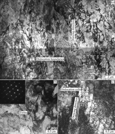
Fig.2 Microstructures of deformed single crystal copper wires: (a) Extended planar dislocation boundaries; (b) Twins; (c) Some dislocation cells and some boundaries parallel to drawn direction shared by some dislocation cells
For the regions with a large number of dislocation cells sharing boundaries parallel to drawn direction, as shown in Fig.2(c), WR?BEL et al[19] also observed them in the cold rolled single crystal copper in cubic orientation. They proved that in these regions with the boundaries shared by some dislocation cells, the orientation does not change with the larger strains. In the drawn industrial copper wires, the results obtained by electron backscattering diffraction show that[3] if the drawn direction of deformation bands evolves from <100> to <111> during drawing process, the micro- structures in the deformation bands are characterized as boundaries like Fig.2(a). If the drawn direction of deformation bands is <100> and the orientation does not change with strain increasing, the microstructures are characterized as some dislocation cells sharing boundaries parallel to drawn direction like Fig.2(c), which is in good agreement with that found by WR?BEL et al[19].
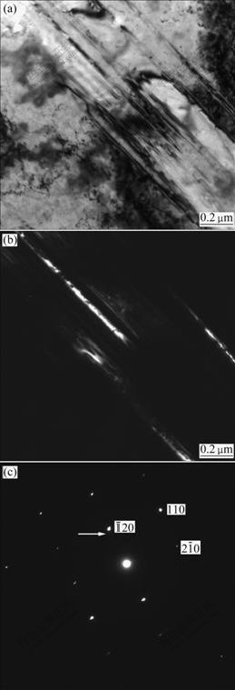
Fig.3 Regions with 9R crystal structure in drawn single crystal copper wires: (a) Bright-field image; (b) Dark-field image; (c) Diffraction pattern obtained from regions with thin plates
4.2 Polytypism of drawn single copper wires
Polytypism can be considered as a specific type of polymorphism in one dimension. The term ��polytypism�� refers to a part of a crystal exhibiting a close-packed structure (or other structure that is composed of a successive stacking of atomic layers) which results from different stacking sequences of the constituent atomic layers. To reflect different translations of close-packed plane with respect to an adjacent plane, a kind of symbol is proposed[13], where the digit expresses the number of close packed layers in the smallest repeated unit and the letter specifies the unit cell symmetry: C for cubic, H for hexagonal, R for rhombohedral. Then, FCC structure is represented by 3C, stacking sequence of close-packed layers in 3C corresponds to ����abc���� and the stacking sequence of close-packed layers in 9R corresponds to ����abcbcacab����. In copper, the polytypes reported are 12R, 4H, 9R[7,10] structures. The diffraction pattern in Fig.3(c) only corresponds to that of 9R type.
Crystal structure transformation may take place only when the energy difference of the two crystal structures is not too large[8]. In fact, the energy difference between FCC and 9R type structure is rather small and is about 0.50 mRy/atom from ab initio calculations on copper[7]. Thus, 9R phase of copper is frequently observed at tilt sub-boundaries in annealed polycrystalline Cu reported by ERNST et al[7-8], in pure Cu in form of precipitates in Fe-Cu and Fe-Cu-Ni alloys by OTHEN et al[11]. Recently, 9R structure has also been observed by DYMEK et al[13] in deformation single crystal copper bar that is uniformly rolled to 50% reduction in thickness and compressed in a channel die to a further 30% reduction. This study is the first time to show that 9R structure can also be presented in the drawn single crystal copper wires.
In the cold drawn wires, 9R-type polytypes have the plate-like features, as shown in Figs.3(a) and 3(b), which is very similar to twins. Although deformation twins were also observed in deformed copper recently[20], the formation mechanism of 9R-type polytypes should not be a pole mechanism. If the formation of a polytype forms in the pole mechanism, Shockley dislocations on parallel slip planes should introduce a stacking fault on two consecutive {111} planes, but not on the third one. This would require the Burgers vector of the pole dislocation to alter during the course of 9R formation, which is impossible. Actually, 9R phase of copper is frequently observed in samples with martensitic transformation, for example, in Cu-Zn and Cu-Al alloys [12]. An alternative mechanism, which was proposed for the explanation of FCC-hexagonal close-packed (HCP) phase transformation or martensitic transformation, is based on a coupled emission of dislocations from a boundary in order to form the nucleus of a new plate-like phase. Contrary to the pole mechanism, the mechanism of the coupled emission of Shockley dislocations from boundaries resulting from deformation may be more reasonable to explain the formation of 9R polytypes in the cold drawn industrial single copper wires.
5 Conclusions
1) The typical microstructures in drawn industrial single copper wires mainly include extended planar dislocation boundaries, a small fraction of twins and regions with a small fraction of dense dislocation and some dislocation cells sharing boundaries parallel to drawn direction.
2) Besides the typical microstructures, 9R structure configurations have also been observed in the wires.
3) The formation of 9R-type polytypes in the wires is based on the coupled emission of Shockley dislocations from boundaries.
References
[1] OHNO A. Continuous casting of single crystal ingots by the O.C.C. process [J]. Journals of Metals, 1986, 38: 14-16.
[2] YAN Wen, CHEN Jian, FAN Xin-hui. Effects of grain boundaries on electrical property of copper wires [J]. Trans Nonferrous Met China, 2003, 13(5): 1075-1079.
[3] CHEN Jian, YAN Wen, WANG Xue-yan, FAN Xin-hui. Microstructure evolution of single crystal copper wires in cold drawing [J]. Science in China (Series E), 2007, 50(11): 736-748. (in Chinese)
[4] XU Zhen-ming, LI Jian-guo, LI Jin-shan, FU Heng-zhi. Mechanical properties and electrical resistivity of continuous casting single crystal copper [J]. The Chinese Journal of Nonferrous Metals, 1999, 9(3): 577-581. (in Chinese).
[5] FAN Xin-hui, WEI Peng-yi, LI Jian-guo, FU Heng-zhi. Effects of technological parameters on surface quality of single crystal Al wire made by continuous casting [J]. The Chinese Journal of Nonferrous Metals, 1997, 7(1): 134-137. (in Chinese)
[6] FAN Xin-hui, LI Jian-guo, FU Heng-zhi. Electrical property of CCSC aluminum wire [J]. The Chinese Journal of Nonferrous Metals, 1999, 9: 87-90. (in Chinese)
[7] WOLF U, ERNST F, MUSCHIK T, FINNIS M W, FISCHMEISTER H F. The influence of grain boundary inclination on the structure and energy of sigma-3 grain boundaries in copper [J]. Philos Mag A, 1992, 66: 991-1016.
[8] ERNST F, FINNIS M W, KOCH A, SCHMIDT C, STRAUMAL B, GUST W. Structure and energy of twin boundaries in copper [J]. Z Metallkd, 1996, 87: 911-922.
[9] SCHMIDT C, ERNST F, FINNIS M W, VITEK V. Prediction and observation of the bcc structure in pure copper at a sigma-3 grain boundary [J]. Phys Rev Lett, 1995, 75: 2160-2163.
[10] ERNST F, FINNIS M W, HOFMANN D, MUSCHIK T, SCONBERGER U, WOLF U. Theoretical prediction and direct observation of the 9R structure in Ag [J]. Phys Rev Lett, 1992, 69: 620-623.
[11] OTHEN P J, KENKINS M L, SMITH G D W, DHYTHIAN W J. Transmission electron microscope investigations of the structure of copper precipitates in thermally-aged Fe-Cu and Fe-Cu-Ni [J]. Philosophical Magazine Letters, 1991, 64: 383-391.
[12] CORNELIS I, WAYMAN S M. Phase transformations in metastable �¡� Cu-Zn alloys (I): Martensitic transformations [J]. Acta Metal, 1974, 22: 291-301.
[13] DYMEK S, WR?BEL M. Polytypism in copper single crystals deformed at room temperature [J]. Mater Chem and Phys, 2003, 81: 552-554.
[14] HANSEN N. Cold deformation microstructure [J]. Mater Sci Techn, 1990, 6: 1039-1047.
[15] KUHLMANN-WILSDORF D. Theory of plastic deformation: Properties of low energy dislocation structure [J]. Mater Sci Eng A, 1989, 113: 1-41.
[16] HANSEN N, HUANG X, PANTLEON W, WINTHER G. Grain orientation and dislocation patterns [J]. Philosophical Magazine, 2006, 86: 3981-3994
[17] HUANG X. Characterization of nanostructured metals produced by plastic deformation [J]. J Mater Sci, 2007, 42: 1577-1583.
[18] JAKOBSEN B, POULSEN H F, LIENERT U, ALMER J, SHASTRI S D, S?RENSEN H O, GUNDLACH C, PANTLEON W. Formation and subdivision of deformation structures during plastic deformation [J]. Science, 2006, 312: 889-892.
[19] WR?BEL M, DYMEK S, BLICHARSKI M, GORCZYCA S. Dislocation microstructure and texture development in rolled copper single crystals [J]. Z Metallkd, 1994, 85: 415-425.
[20] HUANG C X, WANG K, WU S D, ZHANG Z F, LI G Y, LI S X. Deformation twinning in polycrystalline copper at room temperature and low strain rate [J]. Acta Materialia, 2006, 54: 655-665.
Foundation item: Project(50771076) supported by the National Natural Science Foundation of China; Project(07JK274) supported by the Education Department of Shaanxi Province, China
Corresponding author: YAN Wen; Tel: +86-29-83208009; E-mail: yanwen@xatu.edu.cn
DOI: 10.1016/S1003-6326(08)60236-8
(Edited by YANG Bing)
Abstract: By using transmission electron microscopy, the microstructures of drawn industrial single crystal copper wires produced by Ohno Continuous Casting(OCC) process were analyzed. The results show that the typical microstructures in the wires mainly include extended planar dislocation boundaries, a small fraction of twins and some dislocation cells sharing boundaries parallel to drawn direction. Besides the typical microstructures, 9R structure configurations were observed in the wires. The formation of 9R polytypes may be caused by the coupled emission of Shockley dislocations from a boundary.
