
J. Cent. South Univ. (2017) 24: 912-920
DOI: 10.1007/s11771-017-3493-x

A new multilevel voltage source inverter configuration with minimum number of circuit elements
Mohammad Reza Jannati Oskuee1, Masoumeh Karimi1, Yahya Naderi2,
Sajad Najafi Ravadanegh2, Seyyed Hossein Hosseini2
1. Smart Distribution Grid Research Lab., Electrical Engineering Department, Azarbaijan
Shahid Madani University, Tabriz, Iran;
2. Faculty of Electrical and Computer Engineering, University of Tabriz, Tabriz, Iran
 Central South University Press and Springer-Verlag Berlin Heidelberg 2017
Abstract:
An advanced configuration for multilevel voltage source converters is proposed. The proposed converter is able to apply asymmetrical DC sources. The configuration of the proposed inverter is well designed in order to provide the maximum number of voltage levels in output terminals using lower number of circuit devices. The authority of the proposed inverter versus the conventional H-bridge cascaded inverter and the most recently introduced ones, is verified with a provided comparison study. The proposed inverter is able to generate the desired voltage levels using a lower number of circuit devices including power semi-conductor switches, IGBTs, diodes, related gate driver circuits of switches and DC voltage sources. As a result, the total cost and installation area are considerably reduced and the control scheme gets simpler. To confirm the feasibility of the proposed multilevel structure, both the simulation and experimental results are provided and compared which shows good agreements.
Key words:
1 Introduction
Multilevel inverter was introduced in early 1980s by NABAE et al [1]. It has attracted attentions of many researchers so far. Multilevel inverters can synthesize several DC voltage sources to create a semi sundial AC voltage and they are the preferred options in many industrial applications and academic research fields in the process of DC/AC power conversion. Multilevel inverter has been absorbed a great deal of ever increasing attention. As a resulting, many new contributions and new commercial topologies have been reported in the last few years and this is still a technology under improvement. An array of power semiconductor switches, diodes and DC power supplies has formed the fundamentals of the multilevel inverter. Multilevel voltage source inverter (MVSI) is to generate the stepwise output voltage waveform by synthesizing DC voltage sources connecting to input side. As the number of DC links in input side becomes more and more, the output steps increases as well and the output waveform gets much closer to sinusoidal waveform. The sinusoidal waveform of multilevel inverters can offer substantial benefits compared to three-level inverters, including higher power quality, lower harmonic components, better electromagnetic interface, higher amplitude of fundamental component, higher efficiency, lower harmonic distortion, lower switching losses and lower dv/dt [1-6]. Moreover, the quality of multilevel inverters output power can be affected by the modulation strategy used. PWM and SVPWM methods are the most common approaches enabling to generate the desired voltage waveform [7, 8]. Inverter��s output power quality, including harmonic spectra, the total harmonic distortion (THD) of output waveform is detailed in different international standards, like IEEE-929, IEEE-1547 and EN-61000-3-2. Commonly, multilevel inverters are divided into three families: diode clamped (DCM), flaying capacitor (FCM) and cascaded H-Bridge (CHB) multilevel inverter. DCM has considerable problems with unequal current stresses and voltage unbalancing [9]. FCM had little influence on the industry mainly because higher switching frequencies are compulsory to preserve the capacitors properly balanced and also the requirement of initialization of the FC voltages [10]. Modularity, easier controllability and higher reliability are the properties that distinguish the CHB inverter from the other mentioned structures. The main drawbacks associated with CHB inverter, are their circuit complexity, higher number of power switches and a great number of DC voltage sources. From the aspect of DC source values, multilevel inverters are divided into two groups. Some topologies are based on the using insulated DC voltage sources with equal values (symmetric topology) and some others are based on using insulated DC voltage sources with various values (asymmetric topology), in order to obtain more output voltage levels. However, providing DC voltage sources with different values can be costly and makes the topologies difficult to be realized. In symmetric multilevel inverters, the value of all DC voltage sources is equal leading to easier realization and lower design costs. However, the symmetric topologies can produce lower number of voltage levels in comparison with the asymmetric topologies. In multilevel structures, the number of required circuit devices including DC voltage sources, power semi-conductor switches and related gate driver circuits of switches versus the output voltage levels is significant, because the overall costs, circuit size, reliability and control complexity are directly dependent on them. So, high number of components in multilevel inverter is the main concern that the advanced topologies of MVSIs try to lower it. In this regards, it is a useful idea to suggest new multilevel inverter topologies with higher performance by reducing the number of required components. As a result, a lot of efforts have been done by researchers to meet this requirement. To the moment, different cascaded multilevel inverters have been reported [11-21]. In Ref. [11], two different algorithms were proposed to define the magnitudes of DC voltage sources in CHB. Using asymmetrical DC sources can increase the number of output voltage levels. Novel MVSIs have been reported in Refs. [12, 13]. These inverters use bidirectional switches. Each bidirectional switch consists of two IGBTs and two diodes. If these IGBTs are connected as common emitter, then for each bidirectional switch, only one gate driver circuit is needed. The main novelty of the converter is about the reduced number of switches compared to CHB. This improvement causes a reduction on gate drive circuits. But, these topologies encounter with higher peak inverse value (PIV, Vpi) compared to CHB. The topology presented in Ref. [14], uses unidirectional switches. For unidirectional switches the number of gate drivers is equal to the number of switches. The numbers of switches and gate driver circuits are less than conventional CHB but the total PIV is more. A novel MVSI, called semi-cascaded inverter, has been reported in Ref. [15]. The main novelty of this converter is about the reduced number of IGBTs and switches compared to CHB. It is known that reducing the number of switches from the conventional inverters imposes an undesired increase in total PIV value. With proper connection of power switches to DC voltage sources, this increase can be limited. Comparatively, the PIV of Ref. [15] is increased compared to that of CHB. But, it must be mentioned that, since the number of IGBTs, switches and gate driver circuits are reduced significantly, an increase in total PIV is acceptable and can be neglected while this increase cannot detract from its values of obtained benefits from reductions. A novel MVSI has been suggested in Ref. [16] that reduces the power components compared to CHB resulting higher PIV. But its PIV is less than those proposed in Refs. [12, 13]. The topology presented in Ref. [17] uses both unidirectional and bidirectional switches where the number of gate drivers is lower than the switches. This inverter uses the same number of IGBTs with the one presented in Ref. [16], but its PIV is lower. The proposed MLI in Ref. [18] reduces the requirements for power devices in comparison with Ref. [17] while having higher PIVs. Recently, novel MVSIs have been suggested. The required power devices for the reported inverters in Refs. [19, 20] are lower compared to CHB and these inverters have kept the PIV equal to CHB. The proposed inverter of Ref. [21] is the reconfiguration of Ref. [15] resulting in lower PIV. The main contribution of this work is to propose a novel configuration for the multilevel voltage source inverter. This topology is inspired of the idea behind conventional CHB. This inverter can generate a large number of steps using lower number of circuit devices compared to conventional CHB and the presented CHB based inverters in Refs. [11-21]. Owing the lower number of requirements for circuit devices, the total costs and the installation area are significantly reduced and the control scheme gets simpler as well. In order to validate the superiority of the proposed multilevel inverter, a full comparison is provided. Based on these comparisons, the proposed inverter requires minimum numbers of DC voltage sources, power switches, IGBTs, power diodes and driver circuits. The remainder of this work is organized as follows: the structure and details of proposed topology are described item by item in section 2. A full comparison between the suggested inverter and the well-known symmetric inverters is represented in section 3. Both simulation and experimental outcomes are given in section 4. Finally, section 5 represents the conclusion.
2 Proposed configuration
The overall view of the proposed MVSI is represented in Fig. 1. The proposed inverter is constituted of series connections of several DC links associated with an independent DC voltage source and related switches. The mentioned independent DC voltage source is pointed by Vs. The value of Vs is selected according to the number of DC sources. In other words, the value of Vs is the function of the number of DC voltage sources. The switches are well configured, so that the proposed inverter can generate all possible voltage steps with the value of positive and negative in the output. In the proposed inverter, both unidirectional and bidirectional switches are used. Each unidirectional switch consists of an IGBT and an anti-parallel fast recovery diode and a gate driver circuit while bidirectional one includes two IGBTs, two anti-parallel fast recovery diodes and one gate driver circuit if common emitter configuration is used. However, both unidirectional and bidirectional power switches conduct current in both directions. Gate driver circuit is to produce the required switching pulses. The overall view of the used switches in the proposed inverter is shown in Fig. 2.
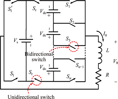
Fig. 1 Proposed MVSI
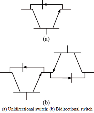
Fig. 2 Type of switch used to implement proposed inverter:
As illustrated in this figure, the proposed topology is composed of n-isolated DC voltage sources. These DC voltage sources can be prepared by rectifiers connected to isolated transformers fed from AC voltage sources, renewable sources like fuel cell, photovoltaic or with energy storage devices, like batteries [22]. It is notable that in the proposed MVSI except Vs, all the required DC voltage links must be equal in value (Vdc). The quality of the output voltage may be deteriorated due to the inequality of DC voltage sources and as a result of inequality of voltage levels. In this regards, undesired harmonics can be generated in the output voltage. In whatever way, the notable point is that producing balanced DC voltage sources is the same problem among all symmetric inverters. In some cases, supplementary circuits, to provide equal DC voltages, are required. For instance, if the PV panels are employed as DC voltage sources, they have already equipped with DC/DC converters for voltage level adjustments. The DC voltage sources can be produced by using transformers and rectifiers. Nevertheless, the undesired changes in the DC voltage sources can be compensated by complementary modulation strategies [23, 24]. The implementation of these methods needs the manipulation of the inverters hardware by additional devices and circuits, and makes the control scheme more intricate. As proposing a novel structure for multilevel inverters is the main goal of this work, countervailing differences of DC voltages which can be done by proper modulation methods are not taken into consideration. A provided output phase voltage is synthesized by individual voltages of DC power supplies. The greatest amount of output voltage (Vo,max) of the introduced topology can be calculated by the following equation:
 (1)
(1)
where the number of DC sources is pointed by n. As noted before, the value of Vs is directly dependent on the number of DC voltage sources. In this regards, the following fundamental constraint must be satisfied in Vs adjustments:
 (2)
(2)
If Vs is considered to be equal to Vdc, the maximum voltage can be calculated by Eq. (3). This method is known as symmetric inverter.
 (3)
(3)
In developed (asymmetric) mode, with assuming Vs=nVdc, a considerable increase can be obtained in the maximum voltage magnitude. The maximum voltage magnitude in developed mode can be calculated as
 (4)
(4)
Then, the number of output voltage levels (m) is given by the following equation:
 (5)
(5)
Therefore,
 (6)
(6)
In other words, the values of n and m must gratify the given relationship:
 (7)
(7)
When considering that all DC sources have equal values, increasing the number of DC voltage sources is the only solution to reach a definite value in the numbers of output voltage levels. However, in developed mode by setting Vs to its maximum possible magnitude, without any manipulation on inverters hardware, a considerable increase can be obtained in the number of output voltage levels. Equation (7) validates this fact that a substantial increase can be obtained in the number of output voltage levels by defining the maximum possible value for Vs. In the suggested inverter, the number of required switches (Nswitch) is calculated by
 (8)
(8)
The relationship between NSwitch and m is as follows:
 (9)
(9)
In the proposed converter, only four switches are unidirectional and the rest of them are bidirectional ones. So, the number of IGBTs can be evaluated by
 (10)
(10)
The following equation represents the relationship between NIGBT and m:
 (11)
(11)
The required switching pulses for each switch are produced by the related gate driver circuit. So, the number of gate driver circuits is equal to the number of switches. Then,
Ndriver=Nswitch (12)
One important problem in multilevel inverters is the voltage rating of power switches. The PIV of all switches is calculated by the following equation:
 (13)
(13)
So, the below formulations are used to calculate the total PIV in both symmetric and asymmetric proposed inverters, respectively:
 (14)
(14)
 (15)
(15)
For simplicity, when it is required to generate mlevels in output voltage, the number of required DC sources must be obtained using Eq. (7). It is obvious that applying developed inverter is frugal. Considering developed mode, the magnitudes of n-1 number of DC voltage sources are equal to Vdc and one other is nVdc. However, in symmetric mode, magnitudes of all DC voltage sources are equal to Vdc. So, developed mode leads to lower number of DC voltage sources, power semi-conductor switches and gate driver circuits. So, the overall costs and circuit size are reduced and the reliability is enhanced and the control method gets simpler as well. Various switching states of the suggested developed topology, for each output voltage step are represented in Table 1 where ��1�� represents that the relevant switch is turn-on and ��0�� represents the off state.
3 Comparison of proposed inverter with other multilevel inverters
It is obvious from the aforementioned discussions that implementing developed (asymmetric) inverter in comparison to the proposed symmetric inverter is more commodious and is more efficient from the technical point of view. As discussed, in multilevel voltage source structures the numbers of required circuit devices including DC voltage sources, power semi-conductor switches and related gate driver circuits of switches versus the output voltage levels are significant, because the overall costs, circuit size, reliability and control complexity directly depend on them. Assuming 19-level in output voltage for a test case, it is found that in symmetric mode, the number of DC voltage sources is 9, the number of switches and so gate driver circuits both are 13 and the total PIV is 76. But considering proposed developed inverter, these numbers are 5, 9 and 44, respectively. This comparison can be expanded to all range of output voltage levels, which will always keep the results similar. So, the proposed developed inverter can generate all desired voltage levels by lower costs, a minimum size and so lower installation area, easier control scheme and higher reliability. In order to compare the suggested developed configuration with CHB and the recently proposed inverters, it is fair to assume that the maximum output voltage is equal for all the mentioned inverters. So, the comparison of MVSIs is discussed versus output voltage levels. It is pointed out that all the inverters participated in comparison study and their different algorithms are shown by R1-R11 in these comparisons. Also the proposed asymmetric inverter is indicated by P. The conventional symmetric cascaded H-bridge inverter is pointed by R1. Moreover, two other algorithms for this inverter have been presented in Ref. [11]. These algorithms are indicated by R2 and R3, respectively. In these algorithms, the values of DC links are as V1=Vdc, V2-��=2Vdc and V1=Vdc, V2-��=3Vdc, respectively. It is pointed out that all other inverters participated in comparison study and their different algorithms are shown by R1-R10 in these comparisons. The conventional symmetric cascaded H-bridge inverter is pointed by R1. Moreover, two other algorithms for this inverter have been presented in Ref. [11]. These algorithms are indicated by R2 and R3, respectively. In these algorithms the values of DC links are as V1=Vdc, V2-��=2Vdc and V1=Vdc, V2-��=3Vdc, respectively. The other reported symmetric multilevel inverters are indicated by R4-R10. The inverter in Ref. [17] is presented by R4; R5 is the other inverter reported in Ref. [15]; R6 is the inverter in Ref. [21]; proposed configurations in Refs. [19, 20] are indicated by R7 and R8, respectively; R9 is the inverter proposed in Ref. [13]; R10 represents the inverter presented in Ref. [12]; the inverter in Ref. [18] is pointed out by R11; the proposed one Ref. [14] is indicated by R12; at the end, R13 is pointed out in Ref. [16]. Number of switches versus number of voltage levels for various MVSI configurations is represented in Fig. 3(a). Assuming that the used switches in the proposed developed inverter are as similar as the ones shown in Fig. 2, then each switch needs one gate driver circuit commanding the switch to conduct or not. Regarding to Fig. 3(a), in the all range of possible voltage levels, the proposed developed topology reduces the requirements for power switches, and so gate driver circuits in comparison with other mentioned solutions. Existing both unidirectional and bidirectional switches in the configuration of proposed inverter causes that the number of IGBTs is different from Nswitch. Figure 3(b) represents the number of IGBTs versus the number of output voltage levels. Figure 3(b) validates that the number of IGBTs is reduced in the proposed developed inverter compared to other mentioned inverters. The number of required DC voltage sources is another parameter that plays a key role in overall inverter costs. Figure 3(c) shows the number of DC voltage sources versus output levels in all mentioned inverters.
Table 1 Various switching states of suggested developed MVSI
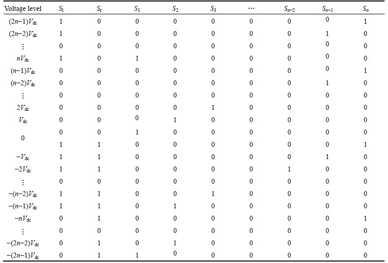
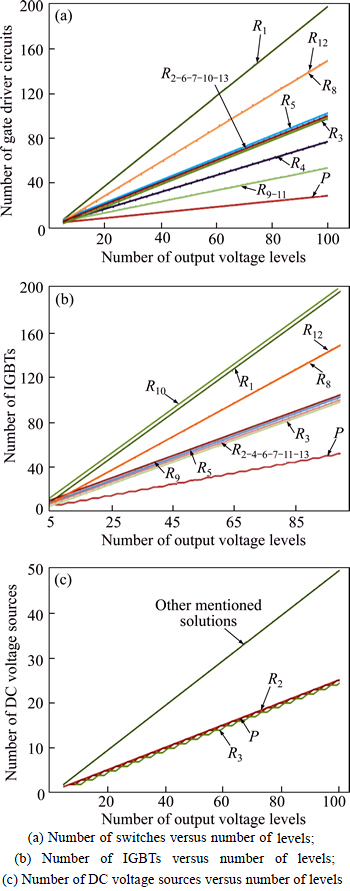
Fig. 3 Comparison of proposed developed topology with other mentioned solutions:
From the comparison studies, it can be said that to realize the same level in the output, the number of required DC voltage sources in the proposed developed inverter is lower. Considering the obtained results from comparison studies given in Fig. 3, it is concluded that the proposed developed inverter reduces the requirements to circuit elements. Another essential parameter which plays a consequential role in overall inverter expense is voltage ratings of power switches. It is known that reducing the number of switches from the conventional inverters imposes an undesired increase in total PIV value. With proper connection of power switches to DC voltage sources, this increase can be limited. Figure 4 depicts the value of considered inverters.
Because of a big reduction in circuit equipment in the proposed inverter, a bit increase in its total PIV compared to some conventional inverters is acceptable and can be neglected, while a reduction in number of switches, gate driver circuits and DC power supplies is achieved.
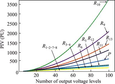
Fig. 4 Total PIV value versus number of levels for proposed developed topology and other mentioned solutions
4 Simulation and experimental results
Since the multilevel inverters are introduced, several switching control strategies have been developed to improve the quality of output power. For instance, fundamental frequency-switching, sinusoidal PWM, selective harmonic elimination (SHE-PWM), space vector PWM (SV-PWM), and others such modulation techniques are used. The benefit of the fundamental frequency-switching scheme is its low switching frequency [25]. For power converters, the total harmonic distortion (THD, Dth) is a popular performance index, which evaluates the quantity of harmonic contents in the output waveform. THD is defined as follows: the ratio of the sum of the RMS value of power of all harmonic components to the RMS value of power of the fundamental frequency component. So, the following equation gives the THD value.
 (16)
(16)
In this equation, n represents the order of the corresponding harmonic, while the sub-index 1 corresponds to the fundamental frequency. Hence,  and
and  are RMS of the nth order harmonic and fundamental harmonic of the output voltage, respectively. Also,
  represents the RMS magnitudes of the output voltage. In above relation, the value of and can be obtained using the following equations, respectively:
 (17)
(17)
 (18)
(18)
where the values of  represent switching angles and can be calculated by
 (19)
(19)
It is clear that the value of THD depends on the number of levels and so switching angles. It is clear that the objective of this work is not THD minimization, and this procedure is only used to generate the output voltage levels. To show the practicability of the proposed multilevel inverter, the simulation studies are presented at first. The converter is simulated by MATLAB software. Then, to validate the feasibility and the good performance of the suggested developed MVSI, experimental results are obtained. Figure 5 shows the circuit diagram of the 19-level multilevel inverter.
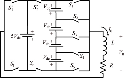
Fig. 5 Circuit diagram of proposed 19-level multilevel inverter
To provide the DC voltage links, the adjustable DC sources existing in the laboratory have been used.Table 2 represents the main parameters of implemented circuit.
Table 3 illustrates the switching states of the developed 19-level suggested inverter.
The voltage and current waveform of the simulated 19-level developed inverter are shown in Fig. 6.
Table 2 Parameters of implemented inverter
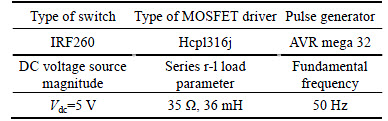
Table 3 Switching states of proposed asymmetric 19-level inverter
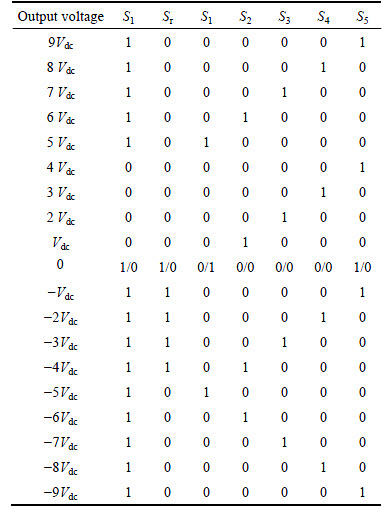

Fig. 6 Voltage and current waveforms (a) and harmonics content of voltage (b) of proposed developed 19-level inverter
It can be seen that all the voltage levels can be generated in the suggested inverter, which validates the practicability of the proposed inverter. To confirm the feasibility of the suggested multilevel inverter, the measured output voltage and current waveforms of implemented single phase prototype of the developed 19-level proposed inverter are shown in Figs. 7(a) and (b).
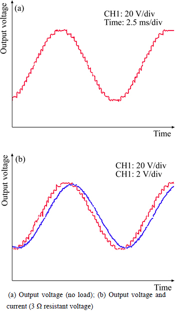
Fig. 7 Experimental results of implemented proposed 19-level inverter:
It can be seen that the provided results confirm that the proposed developed inverter is able to generate the desired output voltage waveform. These figures show good agreements in the simulation and experimental results. The negligible difference between the magnitudes of the simulation and experimental results is due to voltage drops in switches in the prototype.
5 Conclusions
The contribution of this work is to propose an advanced configuration for multilevel voltage source inverters. This inverter reduces the number of devices, including its power semiconductor switches, IGBTs, related gate driver circuits of switches and DC voltage sources. The provided comparison study among suggested inverter, CHB and the recently proposed converters shows the superiority of the proposed inverter over the mentioned topologies. To implement the inverter circuit, the lower number of required devices results in substantial reduction in total costs and installation area, higher reliability and simpler control scheme. To confirm the practicability of the proposed inverter, a prototype of the proposed topology has been implemented. Finally, simulation and experimental results are compared with each other and the provided comparison shows that the obtained results are in good agreements.
References
[1] OSKUEE M R J, KARIMI M, RAVADANEGH S N, GEVORK B. An innovative scheme of symmetric multilevel voltage source inverter with lower number of circuit devices [J]. IEEE Trans Ind Electrons, 2015, 62(11): 6965-6973.
[2] BANAEI M R, KAZEMI F M, OSKUEE M R J. New mixture of hybrid stacked multicell with half-cascaded converter to increase voltage level [J]. IET Power Electron, 2013, 6(7): 1406-1414.
[3] BANAEI M R, OSKUEE M R J, KAZEMI F M. Series H-bridge with stacked multicell inverter to quadruplicate voltage levels [J]. IET Power Electron, 2013, 6(5): 878-884.
[4] AJAMI A, OSKUEE M R J, KHOSROSHAHI M T, MOKHBERDORAN A O. Cascade multi-cell multilevel converter with reduced number of switches [J]. IET Power Electron, 2014, 7(3): 552-558.
[5] BABAEI E, HOSSEINI S H, GHAREHPETIAN G B, TARAFDARHAQUEA M, SABAHI M. Reduction of dc voltage sources and switches in asymmetrical multilevel converters using a novel topology [J]. Electric Power Systems Research, 2007, 77: 1073-1085.
[6] HINAGO Y, KOIZUMI H. A single-phase multilevel inverter using switched series/parallel DC voltage sources [J]. IEEE Trans Ind Electrons, 2010, 57(8): 2643-2650.
[7] AJAMI A, MOHAMMADZADEH B, OSKUEE M R J. Utilizing the cuckoo optimization algorithm for selective harmonic elimination strategy in the cascaded multilevel inverter [J]. ECTI Transactions on Electrical Eng, Electronics, and Communications, 2014, 12(1): 8-16.
[8] DAS S, NARAYANAN G, PANDEY M. Space-vector-based hybrid pulse width modulation techniques for a three-level inverter [J]. IEEE Trans Power Electron, 2014, 29(9): 4580-4591.
[9] DEEPAK E S, ANIL C S, SANJAY S, FEBI C, SAJINA K R. A novel multilevel inverter topology based on multi-winding multi-tapped transformers for improved wave shape requirements [C]//Power Electronics (IICPE), 2010 India International Conference on. 2011: 28-30.
[10] KOURO S, MALINOWSKI M, GOPAKUMAR K, POU J, FRANQUELO L G, BIN WU, RODRIGUEZ J, PEREZ M A, LEON J I. Recent advances and industrial applications of multilevel converters [J].IEEE Trans Ind Electrons, 2010, 57(8): 2553-2580.
[11] LAALI S, ABBASZADEH K, LESANI H. A new algorithm to determine the magnitudes of dc voltage sources in asymmetric cascaded multilevel converters capable of using charge balance control methods [C]// IEEE International Conference on Electrical Machines and Systems (ICEMS). Incheon: IEEE, 2010: 56-61.
[12] BABAEI E, HOSSEINI S H, GHAREHPETIAN G B, TARAFDAR M, HAQUEA, SABAHI M. Reduction of dc voltage sources and switches in asymmetrical multilevel converters using a novel topology [J]. Electric Power Systems Research, 2007, 77(8): 1073-1085.
[13] BABAEI E. A cascade multilevel converter topology with reduced number of switches [J]. IEEE Trans Power Electrons, 2008, 23(6): 2657-2664.
[14] CHOI W K, KANG F S. H-bridge based multilevel inverter using PWM switching function [C]// 31st International Telecommunications Energy Conference (INTELEC). Incheon: IEEE, 2009: 1-5.
[15] HOSSEINI S H, FARAKHOR A, HAGHIGHIAN S K. New cascaded multilevel inverter topology with minimum number of switches and sources [J]. Energy Conversion and Management, 2009, 50(11): 2761-2767.
[16] HIROTAKA Y, KOIZUMI H. A single-phase multilevel inverter using switched series/parallel DC voltage sources [J]. IEEE Trans. Ind. Electrons, 2010, 57(8): 2643-2650
[17] BANAEI M R, SALARY E. New multilevel inverter with reduction of switches and gate driver [J]. Energy Conversion and Management, 2011, 52(2): 1129-1136.
[18] KANGARLU M F, BABAEI E. LAALI S. Symmetric multilevel inverter with reduced components based on non-insulated dc voltage sources [J]. IET Power Electron, 2012, 5(5): 571-581.
[19] KANGARLU M F, BABAEI E. Cross-switched multilevel inverter: an innovative topology [J]. IET Power Electron, 2013, 6(4): 642-651.
[20] AJAMI A, REZA J O M, TOOPCHI KHOSROSHAHI M, MOKHBERDORAN A. Cascade-multi-cell multilevel converter with reduced number of switches [J]. IET Power Electron, 2013, 7(3): 552-558.
[21] BANAEI M R, OSKUEE M R J, KHOUNJAHAN H. Reconfiguration of semi-cascaded multilevel inverter to improve systems performance parameters [J]. IET Power Electron, 2014, 7(5): 1106-1112.
[22] BABAEI E. Optimal topologies for cascaded sub-multilevel converters [J]. J Power Electron, 2010, 10(3): 251-261.
[23] NAUMANEN V, LUUKKO J, SILVENTOINEN P, PYRHONEN J, SAREN H, RAUMA K. Compensation of DC link voltage variation of a multilevel series-connected H-bridge inverter [J]. IET Power Electron, 2010, 3(5): 793-803.
[24] LU S, MARIETHOZ S, CORZINE K A. Asymmetrical cascade multilevel converters with noninteger or dynamically changing DC voltage ratios: Concepts and modulation techniques [J]. IEEE Trans Ind Electron, 2010, 57(7): 2411-2418.
[25] LUDOIS D C, REED J K, VENKATARAMANAN G. Hierarchical control of bridge-of-bridge multilevel power converters [J].IEEE Trans Ind Electrons, 2010, 57(8): 2679-2690.
(Edited by YANG Hua)
Cite this article as:
Mohammad Reza Jannati Oskuee, Masoumeh Karimi, Yahya Naderi, Sajad Najafi Ravadanegh, Seyyed Hossein Hosseini. A new multilevel voltage source inverter configuration with minimum number of circuit elements [J]. Journal of Central South University, 2017, 24(4): 912-920.
DOI:https://dx.doi.org/10.1007/s11771-017-3493-xReceived date: 2015-09-17; Accepted date: 2016-03-01
Corresponding author: Sajad Najafi Ravadanegh, Assistant Professor, PhD; Tel: +98-4124327500; E-mail: s.najafi@azaruniv.edu
Abstract: An advanced configuration for multilevel voltage source converters is proposed. The proposed converter is able to apply asymmetrical DC sources. The configuration of the proposed inverter is well designed in order to provide the maximum number of voltage levels in output terminals using lower number of circuit devices. The authority of the proposed inverter versus the conventional H-bridge cascaded inverter and the most recently introduced ones, is verified with a provided comparison study. The proposed inverter is able to generate the desired voltage levels using a lower number of circuit devices including power semi-conductor switches, IGBTs, diodes, related gate driver circuits of switches and DC voltage sources. As a result, the total cost and installation area are considerably reduced and the control scheme gets simpler. To confirm the feasibility of the proposed multilevel structure, both the simulation and experimental results are provided and compared which shows good agreements.
