

Three-dimensional machining of insulating ceramics materials with electrical discharge machining
Yasushi FUKUZAWA1, Naotake MOHRI2, Hiromitsu GOTOH3,Takayuki TANI3
1. Department of Mechanical Engineering, Nagaoka University of Technology, Niigata, Japan;
2. Department of Precision Engineering, The University of Tokyo, Tokyo, Japan;
3. Department of Industrial Information, Tsukuba University of Technology, Tsukuba, Japan
Received 2 March 2009; accepted 30 May 2009
Abstract:
The insulating ceramics were processed with sinking and wire cut electrical discharge machining(EDM). The new technology was named as the assisting electrode method. In the machining, the electrical conductive material was adhered on the surface of insulating workpiece as the starting point of electrical discharge. As the processing operated in oil, the electrical conductive product composed of decomposition carbon element from working oil adhered on the workpiece during discharge. The discharges generated continuously with the formation of the electrical conductive layer. So, the insulating ceramics turn to the machinable material by EDM. We introduced the mechanism and the application of the machining of insulating ceramics such as Si3N4 and ZrO2.
Key words:
insulating ceramics; electrical discharge machining; assisting electrode method;
1 Background
One of the most important issues of the fine ceramics materials was the precise shape machining without generation of micro cracks by the traditional mechanical machining methods. Special machining methods such as laser, ultrasonic and jet water and electrical beam machining have been applied to the ceramics materials. On the other hand, an electrical discharge machining(EDM) is recognized as the process for precision machining of hard and electrically conductive materials. Previously, it has been considered that insulating materials could not be machined by the EDM method. A new machining method of the insulating material by EDM was proposed, which was named as assisting electrode method(AEM)[1-2]. In the AEM method, an electrically conductive thin layer was bonded on the workpiece prior to the discharge process and the electrically conductive products adhered on the workpiece during the discharge process. The electrically conductive products are composed of cracked carbon that formed as a result of the thermal dissolution of the working oil. The removal machining process occurred simultaneously with the formation of the electrically conductive products. Using this method, many insulating ceramics such as Si3N4, SiC, AlN and ZrO2 have been machined to complex shapes in three dimensions with wire electrical discharge machining(WEDM) apparatus.
2 WEDM apparatus and process of machining
Fig.1 shows the machining apparatus for the assisting electrode method by WEDM. The surface of the insulating ceramics is covered with an electrical conductive layer. This contacted layer on the ceramics surface takes the role of the assisting electrode. During the machining process, the workpiece is dipped in kerosene oil. The specially designed control system is used as the power source.
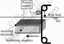
Fig.1 WEDM of insulating ceramics
In the assisting electrode method, it is assumed that the machining process proceeds with two discharge phenomena alternately. One corresponds to make and adhere the electrically conductive layer on the surface of the workpiece. There is a match for the surface modification phenomenon with discharge. The other is responsible for the actual removal machining from the workpiece. Fig.2 shows the typical continuous discharge waveforms of current against voltage in SEDM of insulating ceramics. Among the generation series of normal discharges, the long pulse discharges that had longer discharge duration than the set up value were detected. It was one of the abnormal pulses and usually observed on the EDM process of the high electrical resistance materials. This indicated that the high electrical resistance area was frequently made and discharged during the machining. On the other hand, it was assumed that the normal discharges played the role of the mass remove. As this machining was carried out in the dipped kerosene atmosphere, the carbonized layer was formed. As mentioned above, the principle of this machining composed of two types of processes. One was fabrication of the carbon products on the discharged high electrical resistance area by the long pulse. The other was common mass removal machining by the normal discharge pulse. It was considered that the machining properties of insulating ceramics would be controlled by the ratio of the long pulse on the waveform generation frequency.
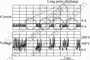
Fig.2 Continuous discharge waveform (Ie=4 A; te=2 ��s; to=32 ��s)
3 Machining properties of ZrO2-20%Al2O3 ceramics
To clarify the effects of the thermal affected area on the EDMed surface, the mechanical strength of WEDMed ceramics was evaluated by four bending test.
3.1 Experiment procedure and material
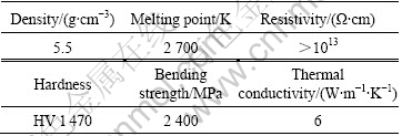
Sintered ZrO2-20%Al2O3 (in mass fraction) ceramics was used as a workpiece. The chemical composition of the workpiece is shown in Table 1. In this workpiece, 20% Al2O3 (in molar fraction) acted as additives. Table 2 shows the mechanical and physical properties of workpiece (catalogue values). Fig.3 shows the schematic illustration of the machining system. The discharge waveforms are observed with the current monitor and recorded on a digital oscilloscope. The commercial WEDM machine with the improved electrical power source circuit was used for this machining. All of the machining was carried out in the working oil.
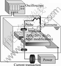
Fig.3 Schematic illustration of WEDM method
Table 1 Chemical composition of workpiece
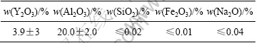
Table 2 Chemical and physical properties of workpiece
The zinc(Zn) coated brass wire was used for the wire tool electrode. Before the discharge, the electrical conductive layer was adhered on the surface of workpiece. The discharge started from the assisting electrode surface. WEDM was carried out under the following conditions: open circuit voltage, Ui=60, 80, 90 V; discharge current, Ie=3 A; electrode polarity being negative.
The 4-point bending tests were applied as followed by JIS R1601 with the WEDMed specimens. It was carried out at room temperature and the crosshead speed was 1 mm/min. Machining properties were evaluated by the removal rate and surface roughness of Rz. Fracture shapes were observed with the optical microscope. The WEDMed surface was polished by the diamond-lapping machine and observed by scanning electrical microscope (SEM) and energy dispersive spectroscope(EDS). The thermal transformation phenomenon was investigated by X-ray diffractometry(XRD).
3.2 WEDM properties and bending strength
The WEDM process of ZrO2-20%Al2O3 ceramics could be accomplished with the Zn coated brass wire as a tool electrode. To investigate the effects of open circuit voltage on the machining properties and strength, the machining was tried under the machining conditions: Ui=60, 80 and 90 V. Fig.4 shows the results of the removal rate on each Ui. The surface roughness results of the WEDMed surface are shown in Fig.5. The bending strength results of WEDMed specimens on each Ui are shown in Fig.6.
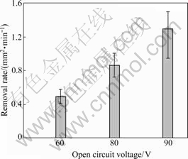
Fig.4 Relationship between removal rate and open circuit voltage
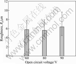
Fig.5 Relationship between surface roughness and open circuit voltage
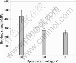
Fig.6 Effects of open circuit voltage on bending strength
The removal rate of WEDMed specimen that had the adhesive electrical conductive layer increased with increasing the Ui value linearily. The surface roughness, Rz, had not so much difference on each condition. The bending strength at Ui=80 V and 90 V decreased below the 1/2 value at Ui=60 V. It is assumed that the thickness of electrical conductive layer affected on the bending strength.
Fig.7 shows the SEM observation results of WEDMed and polished surfaces. It was concluded that micro cracks could not be observed on the WEDMed surface. Fig.8 shows the fracture shapes at Ui=60 V and 90 V. The failure process propagated from the WEDMed surface linearily to compressive stress area. The strength at Ui=60 V that was the highest value in these machining conditions attended to 1/3 value of the ground specimen. It appeared that the strength depended on the structural effects of the WEDMed surface.
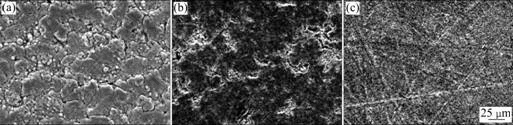
Fig.7 SEM images of polished surface: (a) After WEDM; (b) Polishing 30 ��m; (c) Polishing 65 ��m
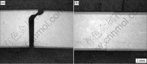
Fig.8 Fracture shapes with different open circuit voltages: (a) 60 V; (b) 90 V
3.3 Structure of electrical conductive layer
Fig.9 shows the observation results of the SEM at the cross sectional WEDMed specimen at each Ui. The thickness of adhered electrical conductive layer could be evaluated from Fig.9. It increased from 30 to 50 ��m with increasing Ui. The removal and adhere process increased simultaneously with increasing Ui. This indicated that the thermal effected zone expanded on the higher Ui condition.
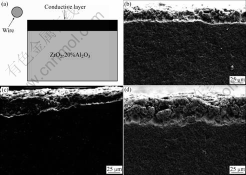
Fig.9 Schematic diagram (a) and SEM images of cross-sectional WEDMed materials at 60 V (b), 80 V (c) and 90 V (d)
Fig.10 shows the observation results of the EDS at Ui=60 V. The electrical conductive layer was composed of three regions. The upper layer was made from carbon(C) and zinc(Zn) elements. Middle layer was composed of zirconium(Zr) and C. Lower layer was Zr and copper(Cu). C element was created from the dissolution of working oil during discharge. Zn and Cu were made from the melting process of wire tool electrode. It was clarified that the ZrO2 resolidified under middle layer of the electrical conductive layer. On the bottomed layer zone, Cu element penetrated into the melted and resolidified ZrO2 body that was the boundary of the machined and conductive layer. Under the bottomed region, the thermal affected zone would be made and the strength of EDMed material would be changed.
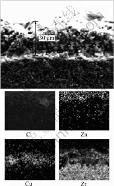
Fig.10 EDS analysis results of WEDMed material (60 V)
3.4 Mechanical strength of EDMed ceramics
To improve the bending strength of WEDMed specimen, mechanical polishing procedure was applied for Ui=60 V. Fig.11 shows the correlation between the polished depth and bending strength. Result of the ground specimen is also plotted in Fig.11. The bending strength increased rapidly with increasing the removal amount. The maximum value was obtained at the removed thickness of 65 ��m. It was larger than the ground specimen value. Over the range of 100 ��m, the bending strength decreased to the same value with the grinded specimen. After polishing, the bending strength kept almost the same value.
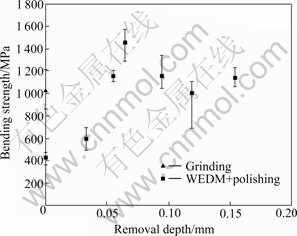
Fig.11 Relationship between bending strength and removal depth
Fig.12 shows the fracture shape of the grinded specimens. The several macro cracks were detected and broken out from the WEDMed surface to the compressed stress area. At the higher bending strength than the ground strength level, the fractured shape looks like a sector. This indicated that any weakened phenomena generated on the WEDMed surface of the thermal affected zone. On the machining of the ZrO2, some structural change would be generated under the WEDMed surface.
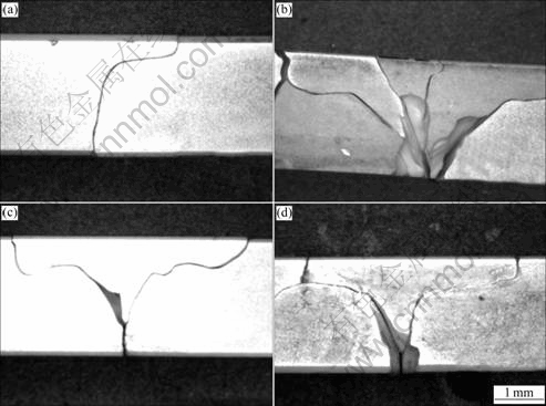
Fig.12 Relationship between fracture shape and polishing depth: (a) 35 ��m; (b) 65 ��m; (c) 130 ��m; (d) 150 ��m
4 Shape machining
The examples of the chair-shaped product (Si3N4) and the temple product (ZrO2) are shown in Fig.13. The shape of this chair was cored from a 50 mm cubic block. Although machining time was about 24 h, it was assumed that the machining would be difficult even if the near net shape method was used, and that mechanical machining was virtually impossible.
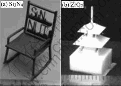
Fig.13 Examples of chair shape product (a) and temple product cored (b) by WEDM from two directions
Machining of axisymmetric shapes could also be machined by WEDM using a rotating workpiece system, as shown in Fig.14. Using the designed lathe that was dipped in oil, the WEDM was carried out to the rotating workpiece. As the wire was scanned in arbitrary paths,the axisymmetric shape could be machined, as displayed in Fig.15. In Fig.15(b), 6 steps could be machined from ![]() 0.1 mm to
0.1 mm to ![]() 0.2 mm.
0.2 mm.
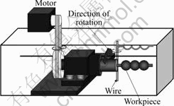
Fig.14 Appearance of WEDM with rotational work piece
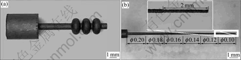
Fig.15 Samples of axisymmetric shape machining: (a) Arbitrary shape; (b) Thin shaft shape
5 Micro machining
Fig.16 shows photographs of the electrode before and after EDM and micro hole drilling result with the electrode on insulating Si3N4 ceramics. In this case that the micro hole was machined with tool electrode of ![]() 0.06 mm, the hole diameter was estimated as approximately 70 ��m and the hole depth was 250 ��m. The wear of the electrode was approximately 125 ��m along the longitudinal direction. Electrode wear occurs mainly along the longitudinal direction, holding the shape of the corner edge.
0.06 mm, the hole diameter was estimated as approximately 70 ��m and the hole depth was 250 ��m. The wear of the electrode was approximately 125 ��m along the longitudinal direction. Electrode wear occurs mainly along the longitudinal direction, holding the shape of the corner edge.
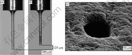
Fig.16 Change of electrode length and EDMed hole on Si3N4 ceramics: (a) Before EDM; (b) After EDM; (c) EDMed hole on Si3N4 ceramics
An example of an EDM produced hole of ![]() 30 ��m is shown in Fig.17(a) and slit machining by scanning EDM is shown in Fig.17(b). On the hole machining of
30 ��m is shown in Fig.17(a) and slit machining by scanning EDM is shown in Fig.17(b). On the hole machining of![]() 30 ��m, machined depth was approximately 200 ��m. A micro hole with a few dozens of micrometers in diameter could be machined into insulating Si3N4 ceramics using this method.
30 ��m, machined depth was approximately 200 ��m. A micro hole with a few dozens of micrometers in diameter could be machined into insulating Si3N4 ceramics using this method.

Fig.17 Formed micro hole (a) and slit shape (b) on Si3N4 ceramics by EDM
6 Conclusions
The machining method of insulating ceramic with SEDM and WEDM was introduced using the Si3N4 and ZrO2 ceramics as the workpiece. The following conclusions were summarized.
1) The thickness of electrical conductive layer, which was made during discharge, increased with increasing the open circuit voltage. The bending strength decreased at the high open circuit voltage condition.
2) The electrical conductive layer was composed of the elements of wire tool electrode and workpiece. The upper zone constructed with carbon and zinc, the middle zone was zirconium and carbon and the lower zone was zirconium and copper.
3) The bending strength was improved using the polishing machining.
4) The three-dimensional complex shape was formed on the insulating ceramics by WEDM.
5) Hole machining and slit machining of dozens of micrometer to insulating ceramics were possible using this method.
References
[1] FUKUZAWA Y, GOTO H, ISOHATA Y, MOHRI N, SAI H, TANI T. Machining technology of insulating Si3N4 ceramics by wire EDM [J]. Australasian Ceramics Society, 2002, 38(2): 120-124.
[2] MOHRI N, FUKUZAWA Y, TANI T, SAITO N, FURUTANI K. Assisting electrode method for machining insulating ceramics [J]. Annals of CIRP, 1996, 45(1): 201-204.
Corresponding author: Yasushi FUKUZAWA; Tel: +81-258-47-9711; E-mail: fukuzawa@vos.nagaokaut.ac.jp
(Edited by YANG Hua)
