

Influence of interfacial reaction between molten SnAgCu solder droplet and Au/Ni/Cu pad on IMC evolution
LI Fu-quan(�Ȫ), WANG Chun-qing(������)
Microjoining Laboratory, School of Material Science and Engineering, Harbin Institute of Technology,
Harbin 150001, China
Received 23 May 2005; accepted 8 August 2005
Abstract:
Intermetallic compounds(IMC) formed at Sn-Ag-Cu solder droplet/pad interface during wetting reaction were investigated. Comparative studies of the IMC evolution during reflow and aging were also conducted. The results show that the wetting reaction between molten solder droplet and pad leads to the formation of Au-Sn compound at interface, but Au element is not fully consumed during wetting reaction. After reflow, all Au layer disappears from the interface, Au element is dissolved into solder and Au-Sn intermetallic compounds are precipitated in the bulk. Reaction between Ni layer and Sn-Ag-Cu solder leads to the formation of (CuxNi1-x)6Sn5 layer at interface during reflow. According to the thermodynamic-kinetic of interfacial reaction, the wetting reaction at solder droplet/pad interface influences the phase selectivity of IMC evolution during reflow and aging process.
Key words:
SnAgCu solder; Au/Ni/Cu pad; solder droplet; intermetallic compounds; interfacial reaction; reflow; ageing;
1 Introduction
The investigation of lead-free assemblies has been recently intensified due to the anticipated legislation to ban the use of lead in electrical and electronic products. Although it has been demonstrated that lead-free soldering is technologically possible and has some advantages, there are many technical issues to be addressed before it is well implemented. The Sn-Ag-Cu alloys are regarded as the most potential lead-free solder system in the electronics. For an actual replacement for the lead-containing solder, reliability of their solder interconnections, which is mainly affected by the intermetallic layers formed at solder/under bump metallurgy(UBM) interface during reflow soldering as well as aging, need to be evaluated thoroughly.
In high-density electronic interconnection, solder bump provides connection between bonding pad of the chips and the metallization on the substrate[1��3]. Molten droplet solder bumping as a new type bumping method is developed in recent years[4��6]. Through controlling the temperature of solder droplet, appropriate bump can be fabricated when molten solder dropped to the metallization pad. Solder alloy redistribution and heating process was carried out simultaneously when droplet contacted with the pad. At the same time, an intermetallic compound(IMC) is formed. During subsequent reflow and ageing process, IMC at solder bump/pad interface continues to grow. It is well known that the presence of IMC between solder bump and pad is an indication of good metallurgical bonding. A thin and continuous IMC layer is an essential requirement for good wetting and bonding, and it produces distinct improvements in mechanical properties of joints. However, due to their inherent brittle nature, too thick of an IMC layer at the solder bump/pad interface may degrade the reliability of the solder joint[7��9].
This study was carried out to obtain a more complete understanding of the reaction between Sn-Ag-Cu solder and Au/Ni/Cu pad. The wetting reactions of the solder droplet with Au-Ni-Cu pad are thoroughly investigated. In an effort to learn how to preserve the integrity of solder joints, the evolution of intermetallic compounds at the bump/pad interface and its influence on solder microstructure are studied in detail.
2 Experimental
The eutectic Sn-3.0%Ag-0.5%Cu(mass fraction)solder ball with a diameter of 0.76 mm was utilized. The substrate used was BT with pads and each pad was 0.6 mm in diameter. The pads had an electroplated Ni/Au surface finish over a Cu conducting trace, with Ni and Au layers of 7 and 2 ?m in thickness, respectively. The Au/Ni two-layer metallization is one of the most common surface finishes for UBM in soldering pads: Ni layer would provide a good barrier to inhibit the excessive growth of Cu-Sn intermetallic compound while the outermost Au layer would offer good wetting and oxidation protection to the layer underneath it. To remove possible organic contami- nation on the pads, substrates were ultrasonic cleaned before experiment.
During the experiment, the solder ball was heated to specific temperature (initial temperature) above melting point of solder and then dropped to the pad at specific height (initial height). The initial distance between the solder droplet and the pad was set as 1mm. Based on the previous study[10], the initial temperature of solder droplet was selected as 400 ��. An infared reflow oven was used during the reflow process. The peak reflow temperature was fixed at 245 ��.The reflow time was 30, 60, 120 and 180 s. Then the as-soldered samples were solid state aged at 125 �� for 1, 4, 9, 16 and 25 d, respectively.
For solder bump/pad interfacial microstructure examination, the samples were cross-sectioned and mounted in epoxy. Then, the cross-sectioned samples were ground and polished carefully. The samples were etched in a solution of 2 mL concentrated HCl, 6 mL concentrated HNO3 and 92 mL H2O. The chemical and microstructural analysis of the samples was obtained by using HITACH-S4700 FEG scanning electron micro- scope(SEM) equipped with energy dispersive X-ray analysis(EDX).
3 Results and discussion 3.1 Interfacial reaction between solder droplet and Au/Ni/Cu pad
The SEM images of interfacial microstructure between Sn-Ag-Cu solder droplet and pad are shown in Fig.1, it can be seen that continuous intermetallic layer emerged at the interface and rod-like compound grew from the continuous intermetallic layer at the solder-pad interface into the solder. As identified by EDX as well as previous research results[9, 11], continuous intermetallic layer close to Ni layer is AuSn2 and Au, and rod-like compound close to solder is AuSn4. The remaining Au at the solder/pad interface indicates that the Au does not react completely. The formation of intermetallic compound at the solder/pad interface indicates that Au is dissolved in the solder after Au layer contacted with the molten solder. On reaching the solubility limit of Au in the molten solder, Au/Sn intermetallics would be formed at the interface. The settle time of solder/pad interface above melting temperature of Sn-Ag-Cu solder is very short. The remaining Au, which can not be dissolved completely, but left at the interface. As compared with Sn-Pb solder, a common feature of Sn-Ag-Cu solder is its high Sn content. As previously stated, the main elements that took part in the interfacial reaction between solder droplet and pad are Au and Sn. The effect of fast reaction between Sn and Au determines rapid formation of Au-Sn intermetallic compounds.
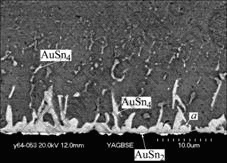
Fig.1 Interfacial microstructures between eutectic Sn-Ag-Cu solder droplet and Au/Ni/Cu pad
It can be observed from Fig.1 that acicular AuSn4 distributes in solder inside the solder joint near the interface, which indicates that IMC breaks off from the interface and migrates into the solder. During the wetting reaction between the molten solder droplet and the pad, the convection effect of the molten solder is distinctive. The faster cooling condition during solidification might also lead to the higher stresses at the interface. Furthermore, Au-Sn compound is brittle. These factors can lead to AuSn4 breaking off and migrating from the interface to the solder inside the solder joint near from interface. On the other hand, the temperature of molten solder is high when it contacts with the substrate. Au is dissolved into solder very rapidly, leading to the formation of Au-Sn compound in the solder bulk. Fig.2 shows EDX spectra of point a at the solder droplet/pad interface as shown in Fig.1. It is worth noting that Cu content (2.16%) in the region adjacent to the interface is higher than that in the solder bulk. In solder bulk, Cu is a minor alloying element. Copper element concentrates in the region adjacent to the interface. Such concentration of Cu has obvious effect on the IMC evolution during the subsequent reflow and aging process.
3.2 Evolution of intermetallic compounds at interface
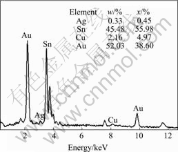
Fig.2 EDX spectrum of point a shown in Fig.1
Fig.3 shows interfacial microstructures between Sn-Ag-Cu solder bump and pad after 30, 120 and 180 s reflow. It can be found that after 30 s reflow, Au layer disappears from the interface and Ni layer comes to contact with the solder. This indicates that the Au layer is consumed entirely. It can be deduced that Au was dissolved completely into solder in less than 30 s. The dissolved Au forms AuSn4 intermetallic compounds that precipitate out of the solder on solidification to form a dense distribution of fine particles distribute through the bulk. After reflow, AuSn4 still can be found in the solder bulk far away from the interface. As shown in Fig.3(d), rod-like and tiny needle-like AuSn4 particles distribute in the solder bulk near the top of the solder bump. As mentioned previously[10], the settle time of solder bump in liquid state was several seconds during reflow process. While during the wetting reaction of solder droplet and pad, the time frame of solder droplet in liquid state was several milliseconds. On the other hand, it is well known that the dissolution rate of Au in molten Sn is high. During reflow, the high dissolution rate of Au led to the remaining Au was dissolved into solder bulk completely.
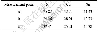
Fig.3 shows that only one type of interfacial compound is found between the solder and Ni layer. After detailed composition analysis by EDX, related EDX quantitative-analysis result of points a, b and c in Fig.3 is listed in Table 1. The IMC at interface is Cu-Ni-Sn ternary compound. The ratio of Cu and Ni to Sn is close to 6��5, and the IMC thus be denoted as (CuxNi1��x)6Sn5. It can be deduced that the IMC at Sn-Ag-Cu solder bump/pad interface after reflow was (CuxNi1��x)6Sn5. The compound (CuxNi1��x)6Sn5 are based on the Cu6Sn5 crystal structure. For Sn-Ag-Cu solder joint after reflow, why the interfacial IMC is (CuxNi1��x)6Sn5 based on Cu6Sn5, and not (Cux- Ni1��x)6Sn5 which based on Ni3Sn4? This is due to the different element constitute at the interface before reflow. In order to answer this question, it is needed to make use of the thermodynamic-kinetic considerations as described elsewhere[12��14].
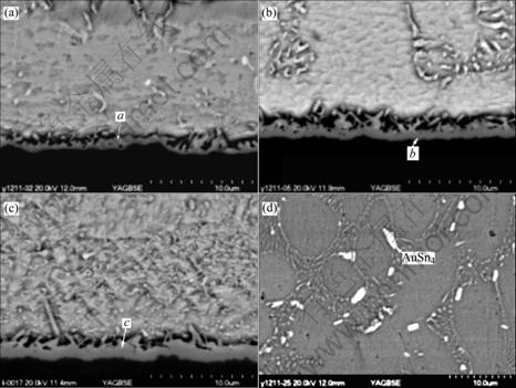
Fig.3 Morphology changes of interface microstructure between eutectic Sn-Ag-Cu solder bump and pad after reflow soldering for 30 s(a), 120 s (b), 180 s (c) and microstructure inside bulk solder far away from interface after 30 s reflow (d)
Table1 Quantitative analysis results for trace points a, b, and c shown in Fig.3(mole fraction, %)
Since the Ag3Sn particles are evenly distributed among the eutectic colonies and no Ag is detected in the interfacial IMC layer, it can be assumed that Ag is not directly involved in the interfacial reactions. The role of Ag in the interfacial reaction can be neglected. Therefore, only the Ni-Cu-Sn system is considered here. Using the optimized dataset, the metastable equilibria of Ni3Sn4 and Cu6Sn5 at 235 �� are calculated and shown in Fig.4. This diagram is calculated by omitting the ternary compound during calculation. The uncertain phase equilibrium is represented by dashed lines in the diagram. Moreover, the temperature used in the study (245 ��) is not far from the temperature of isotherm (235 ��). Therefore, it is credible to use the Cu-Ni-Sn phase diagram to explain the behaviors in current system.
During the soldering, the diffusion of the components of the solder into the Ni layer is much slower than that of Ni into the molten solder. Therefore, it is a good approximation that the ratios of Sn/Cu in the solder virtually do not change with time in the effective joint region[15]. As shown in Fig.4, the composition of the point c is 0.6Cu and 99.3Sn (mass fraction, %, the same below). According to the procedure for predicting the first phase formation in the solder joints[12], if the Cu content in the solder is so small that the connection line across the liquidus line of Ni3Sn4 phase (on the left side of point c), Ni3Sn4 will be the first intermetallic compound to form during the soldering process. But if the Cu content in the solder is higher than 0.6%, the IMC to form is the Cu6Sn5 with some solution of Ni.
Before reflow, it is worth noting that copper element concentrates in the region adjacent to the interface. Such concentration of Cu has obvious effect on the evolution of IMC during the subsequent reflow process. As shown in Fig.2, Cu content (2.16%) in the region adjacent to the interface is higher than that in the solder bulk. So the interfacial IMC was assumed to be Cu6Sn5 with some solution of Ni. From Table 1, it can be found that the Ni content inside (CuxNi1��x)6Sn5 increases with increasing reflow time. Apparently Ni atoms substitute for some of Cu atoms in the Cu6Sn5 phase. As the atomic size difference between Cu and Ni is only 2% and both have the same fcc lattice structure, the substitution of Ni into Cu6Sn5 without causing lattice distortion or new phase formation is reasonable[16].
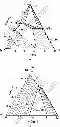
Fig.4 Calculated metastable phase equilibria of Ni3Sn4 and Cu6Sn5 phases at 235 �� (a) and enlarged Sn-corner of (a) (b)[14]
Fig.5 shows morphology changes of interface microstructure between Sn-Ag-Cu solder bump and pad after 120s reflow soldering, and then subject to aging. The interfacial IMC during solid state aging is (CuxNi1��x)6Sn5, which are based on the Cu6Sn5 crystal structure. The thickness of (CuxNi1��x)6Sn5 increases with aging time. As indicated in Fig.6, the thickness of the intermetallic compound is monitored as a function of aging time. The simple theory discussed for the growth of a reaction product by solid state diffusion between reactants originally in contact, predicts that the thickness of IMC layer is proportional to the square root of the aging time. After aging 25 d, the average thickness of the (CuxNi1��x)6Sn5 is found to be 1.9 ?m.
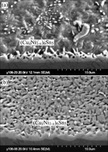
Fig.5 Morphology changes of interface microstructure between Sn-Ag-Cu solder bump and pad after 120 s reflow soldering, and then aged for 9 d (a) and 25 d (b)
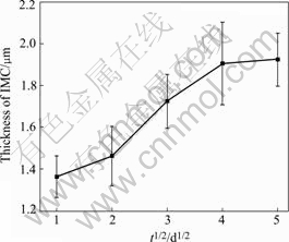
Fig.6 Growth of thickness of (CuxNi1-x)6Sn5 layer with aging time
4 Conclusions
1) After wetting reaction between Sn-Ag-Cu solder droplet and Au/Ni/Cu pad, interfacial microstructure was Au-Sn compound. The continuous intermetallic compound layer close to Ni layer is AuSn2, rod-like compound close to solder is AuSn4.
2) Au layer disappears from the interface, and Au-Sn compounds precipitate in solder bulk during solidification process after reflow. (CuxNi1��x)6Sn5 forms at Sn-Ag-Cu solder and Ni layer during reflow. During aging process, the thickness of (CuxNi1-x)6Sn5 increases with aging time.
3) Copper element concentrated in the region adjacent to the interface during wetting reaction. Such concentration of Cu has obvious effect on the phase selectivity at Sn-Ag-Cu solder/pad interface during reflow.
References
[1] Kloeser J, Coskina P, ASCHENBRENNER A. Bump formation for flip chip and CSP by solder paste printing[J]. Microelectronics Reliability, 2002, 42: 391��398.
[2] Koshoubu N, Ishizawa S, TSUNETSUGU H. Advanced flip chip bonding techniques using transferred micro-solder bumps [J]. IEEE Transactions on Components and Packaging Technologies, 2000, 23(2): 399��404.
[3] LI Li, Thompson P. Stencil printing process development for flip chip interconnect[J]. IEEE Transactions on Electronics Packaging Manufacturing, 2000, 23(3): 165��170.
[4] LIU Q B, ORME M. High precision solder droplet printing technology and the state-of-the-art[J]. Journal of Materials Processing Technology, 2001, 115: 271��283.
[5] HAYES D J, COX W R, GROVE M E. Micro-jet printing of polymers and solder for electronics manufacturing[J]. Journal of Electro Nics Manufacturing, 1998, 8: 209��216.
[6] Baggerman F J, Schwarzbach D. Solder-jetted eutectic PbSn bumps for flip-chip[J]. IEEE Transactions on Components B, 1998, 21(4): 371��381.
[7] Bradley E, Banerji K. Effect of PCB finish on the reliability and wettability of ball grid array packages[J]. IEEE Transactions on Components, Packaging B, 1996, 19(2): 320��330.
[8] Puttlitz K J. Preparation, structure, and fracture modes of Pb-Sn and Pb-In terminated flip-chips attached to gold capped microsockets[J]. IEEE Transactions on Components, Hybrids, and Manufacturing Technology, 1990, 13(4): 647��655.
[9] TU K N, ZENG K. Tin-lead (SnPb) solder reaction in flip chip technology[J]. Mater Sci Eng R, 2001, R34: 1��58.
[10] LI Fu-quan, WANG Chun-qing, TIAN De-wen, TianYan-hong and P.liu. Interfacial reaction between molten 63Sn37Pb droplet and Au/Ni/Cu pad[J]. The Chinese Journal of Nonferrous Metals, 2004, 14(7): 1139��1143.(in Chinese)
[11] TIAN Y H, WANG C Q, GE X S, et al. Intermetallic compounds formation at interface between PBGA solder ball and Au/Ni/Cu/BT substrate after laser reflow processes[J]. Mater Sci Eng B, 2002, B95(1): 254��262.
[12] ZENG K, Kivilahti J K. Use of multicomponent phase diagrams for predicting phase evolution in solder/conductor systems[J]. Journal of Electronic Materials, 2001, 30(1): 35��44.
[13] Kulojarvi K, Vuorinen V, Kivilahti J K. Effect of Dissolution and Intertmetallic Formation on the reliability of FC joints[J]. Microelectronics International, 1998, 15: 20��24.
[14] ZENG K,Vuorinen V, Kivilahti J K. Interfacial reactions between lead-free SnAgCu solder and Ni(p) surface finish on printed circuit boards[J]. IEEE Transactions on Electronics Packaging Manufacturing, 2002, 25(3): 162��167.
[15] R?nk? K J, van Loo F J J, Kivilahti J. The local nomial composition-useful concept for microjoining and interconnection applications[J]. Scripta Materialia, 1997, 37(10): 1575��1581.
[16] Park J K, Yang C W, HA J S. Investigation of interfacial reaction between Sn-Ag eutectic solder and Au/Ni/Cu/Ti thin film metallization[J]. Journal of Electronic Materials, 2001, 30(9): 1165��1170.
Correspondign author: WANG Chun-qing; Tel: +86-451-86418725; E-mail: wangcq@hit.edu.cn
(Edited by LONG Huai-zhong)
