
J. Cent. South Univ. Technol. (2011) 18: 2176-2184
DOI: 10.1007/s11771-011-0960-7![]()
Application of micro/nanoscale thermal radiation to
thermophotovoltaic system
WANG Ai-hua(������)1, 2, CAI Jiu-ju(�̾ž�)1
1. School of Materials and Metallurgy, Northeastern University, Shenyang 110819, China;
2. Department of Mechanical and Aerospace Engineering, Florida Institute of Technology,Melbourne 32901, USA
? Central South University Press and Springer-Verlag Berlin Heidelberg 2011
Abstract:
Thermophotovoltaic (TPV) system has been regarded as one promising means to alleviate current energy demand because it can directly generate electricity from radiation heat via photons. However, the presently available TPV systems suffer from low conversion efficiency and low throughput. A viable solution to increase their efficiency is to apply micro/nanoscale radiation principles in the design of different components to utilize the characteristics of thermal radiation at small distances and in microstructures. Several critical issues are reviewed, such as photovoltaic effect, quantum efficiency and efficiency of TPV system. Emphasis is given to the development of wavelength-selective emitters and filters and the aspects of micro/nanoscale heat transfer. Recent progress, along with the challenges and opportunities for future development of TPV systems are also outlined.
Key words:
1 Introduction
Fast depleting reserves of conventional energy sources have resulted in an urgent need for increasing energy conversion efficiencies and recycling of waste heat. Thermophotovoltaic (TPV) devices have been considered as energy conversion systems, which allow recycling of the waste heat as well as increasing the conversion efficiency. Concern for the environment and global efforts to reduce energy losses has resulted in a growing interest in TPV systems.
TPV systems operate on the principle of photovoltaic effect, in which photons whose energy is greater than the band gap of the TPV cell can create electron�Chole pairs. The photons are considered as the radiant energy emitted by the high-temperature TPV source, which is called a radiator or emitter. A junction between dissimilarly doped semiconductor layers sets up a potential barrier in the cell and separates the photo-generated charge carriers. This separation induces an electromotive force in the cell and results in electric current [1-2]. Depending on the emitter temperature, the performance of TPV systems can be optimized by selectively filtering the thermal radiation using a wavelength-selective emitter or filter, according to the band gap of a TPV cell.
The key advantages of the TPV systems over other energy conversion devices are the versatility of the heat source and the absence of any moving parts. Absence of moving parts, portability and quiet operation have made TPV systems promising for power generation in military applications [3]. Moreover, the spectrum of the emitted radiation can match the band gap of the cells and reduce the amount of unusable radiation, as compared with the conventional PV systems, thereby achieving higher effciencies. A variant of TPV systems called microthermophotovoltaic (MTPV) devices has been developed in recent years as power devices for micro- electromechanical systems (MEMS) [4]. Miniaturization of electronic gadgets, such as notebook computers, cell phones, and iPods, has resulted in increasing demands on the power sources for MEMS devices. This has necessitated the development of such micropower generators [5-7].
However, the most obvious drawbacks of TPV devices are their low conversion efficiency and low throughput due to a large amount of unusable radiation [8]. One possible solution of increasing the power output is the application of the principles of microscale radiation to TPV systems. For example, the efficiency can be increased by using micro/nanostructured emitters and filters. On the other hand, the throughput can be enhanced nearly 10-fold by reducing the distance between the emitter and the TPV cell to sub-wavelength dimensions, namely the near-field theory [9-11]. Since the length scales are comparable to the wavelength, neither the near-field energy enhancement nor the working principles of micro/nanostructured emitters/ filters can be comprehensively explained by conventional radiation heat transfer. Hence, a clear understanding of the principles of microscale radiation is required for the further advancement of TPV technology.
2 Fundamentals of TPV devices
2.1 Operation principle
TPV devices operate based on the principle of photovoltaic effect, the phenomenon in which electromagnetic radiation incident upon a p�Cn junction induces an electromotive force. This requires an internal potential barrier with a built-in electric field to separate the photogenerated electron�Chole pairs. The barrier is formed in a single crystal semiconductor material containing both p- and n-type regions. When the p-type region contains a large concentration of holes with few electrons, and the opposite is true for n-type region, the interface between the two regions is commonly referred to as the junction. Due to the charge concentration gradient, holes from the p-side diffuse into the n-side, whereas the electrons from the n-side diffuse to the p-side. Consequently, the region near the junction (known as the depletion layer) is depleted of majority carriers and contains only ionized dopants. The carrier concentration remains unperturbed in an isolated material beyond the depletion region on both p and n sides.
MAUK and ANDREEV [12] and GONZALEZ- CUEVAS et al [13] presented a typical p-on-n junction In0.2Ga0.8Sb TPV cell. For TPV cells, p-on-n configuration is preferred over n-on-p because the annealing of the ohmic contact to the n-type material results in a short circuit at the cell junction. An antireflection coating of ZnS and MgF2 can be formed on the top of the cell, to reduce the reflection of incident radiation. For an ideal TPV cell, most of the incident energy should be absorbed within the depletion region corresponding to a length of 3����, where ���� is the penetration depth of the incident radiation. When the incident radiation with photon energy greater than the band gap (Eg) of the cell strikes the p�Cn junction, electron�Chole pairs are generated. Those pairs generated in the depletion region are swept by the built-in electric field. These are then collected by the electrodes at the two ends of a TPV cell, thus resulting in drift current. On the other hand, the electron�Chole pairs generated within the diffusion length outside the depletion region can diffuse as minority carriers to the edge of the depletion region, yielding diffusion current [14].
2.2 Quantum efficiency of TPV cell
An important parameter of the cells affecting the performance of TPV systems is their quantum efficiency (��Q), which is defined as the ratio of the number of electron�Chole pairs generated to the number of photons absorbed. If the fraction of the reflected photons is taken into account in the calculation of ��Q, it is called external quantum efficiency. Otherwise, it is called internal quantum efficiency. A comparison was shown of the absorption coefficients and internal quantum efficiencies of In0.2Ga0.8Sb (band gap of 0.63 eV) and In0.53Ga0.47As (band gap of 0.74 eV) cells in the spectral range of 0.5 and 2.5 ��m with a p-on-n type configuration [13, 15-16]. Photons with energy higher than the band gap are mostly absorbed within the depletion region of the cell. These photons can generate useful electron�Chole pair contributing to the quantum efficiency. On the other hand, some of the photons with energy lower than the band gap of the cells are absorbed beyond the depletion region due to longer penetration depth of the material at these wavelengths. These photons cannot generate any electron�Chole pairs and will be dissipated into thermal energy to heat up the cell. In order to reduce the heating, back surface reflectors may be added to the TPV cells to reflect back the low-energy photons [17]. The fast recombination near the surface results in low minority carrier lifetime and reduces the quantum efficiency drastically [18-19].
2.3 Efficiency of TPV systems
Efficiency of any TPV system (��) can be defined as the ratio of the power flux output from the cell (Pout) to the power flux emitted from the radiator (Pemit). The efficiency can also be represented as [20]
![]() (1)
(1)
where Pinc is the flux incident on the TPV cell, ��d is the diode or cell efficiency, and ��f is the efficiency of the filter used in the TPV systems.
Another important factor describing the performance of TPV cells is the fill-factor (��), which is also known as the power usage efficiency. Here, �� is the ratio of the maximum possible power obtained from the cell to the product of short circuit current density (Jsc) and open circuit voltage (Voc) of the cell [2, 21-22]. Mathematically, the fill factor is expressed as [23]
![]() (2)
(2)
The spectral efficiency of the filter is defined as the fraction of total absorbed radiation with energy greater than the band gap of the cell. It can be expressed as [24]
![]()
 (3)
(3)
where �� is the frequency of the emitted radiation; ��g is the band gap frequency given by Eg/h, here h is Planck��s constant; R�� and ���� represent the reflectance and absorptance of the filter, respectively; I is the intensity of radiation emitted from radiator; �� and f are the polar and azimuthal angles, respectively.
An ideal filter is expected to have a high transmittance in the spectral region corresponding to the band gap of the TPV cell and high reflectivity outside the region while having a low absorptance in the entire spectrum. Using a selective band pass filter improves the overall efficiency more than a high- or a low-pass filter. Absorption of photons by the electrodes, electrical interconnects, and other non-power producing areas of the TPV arrays are often referred to as parasitic absorption [25-26]. In order to avoid the absorption, non-power producing areas of the TPV system need to be minimized or coated with a reflective material to recycle the energy back to the radiator.
3 Emitters and filters
A radiator/emitter is a critical component of TPV systems and a wavelength-selective filter is sometimes used for enhancing the performance of TPV devices. The development in microfabrication techniques over the past few years has resulted in further progress in the field of emitters and filters.
3.1 Emitters
Rare-earth oxides were the earliest wavelength- selective emitters considered for TPV applications, especially at high temperatures [27-28]. Rare-earth ions in crystals behave like an isolated ion and emit narrow band radiation due to their atomic structure [29]. Recent progress in micro- and nano-technology has resulted in the use of periodic structures as wavelength-selective emitters in the TPV systems. Because the structural complexity may increase with dimension, the present review introduces TPV emitters in the sequence of 1D, 2D, and 3D structures. An example of 1D structure as a TPV emitter was proposed recently [30]. The advantages of the 1D emitters over their 2D and 3D counterparts are the ease in fabrication and the directional independence of emittance spectra. However, the emittance spectrum shows sharp peaks and is sensitive to emission angle, which prevents simple 1D binary gratings from being used as TPV emitters. A kind of 1D complex grating has recently been proposed to provide an alternative design for the emitter [31].
Recent progresses of 2D tungsten gratings and 3D photonic crystals for TPV emitters are shown in Fig.1. Tungsten is used for most TPV emitters because it is corrosion resistant and can withstand high temperatures. Figure 1(a) shows a 2D tungsten grating used as emitter [32]. The grating has period of 2.0 ��m and depth of 0.3 ��m. The normal emittance of the fabricated structure shows emittance of 0.7 at 1 200 K and ��=1.6 ��m.
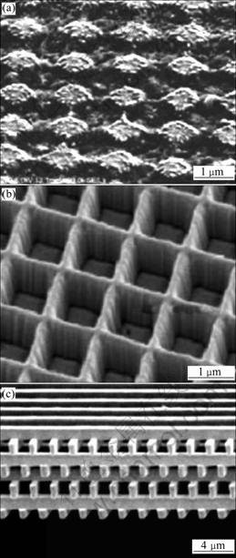
Fig.1 Selective emitters: (a) 2D tungsten gratings; (b) 2D tungsten emitter; (c) 3D tungsten photonic crystals
Figure 1(b) demonstrates another kind of 2D tungsten gratings for TPV emitters [33-34]. The period and the depth of the structure are 1.0 and 0.75 ��m, respectively, while the inner cavity is 0.8 ��m �� 0.8 ��m. The emittance peak at near infrared region is caused by confined modes inside the cavities and is promising for TPV emitters. Figure 1(c) shows the use of 3D tungsten photonic crystals as TPV emitters [34]. The 3D structure composed of multilayered 1D periodic tungsten rods exhibits high spectral emittance (>0.8) in the range from 1.5 to 1.9 ��m. The emittance from the photonic crystal at 1 535 K exhibits a peak power density of 40.5 W/cm2, which is four times greater than that of a blackbody at the same temperature.
3.2 Filters
Many pure dielectric materials and transparent conducting oxides have been used as wavelength- selective filters. Silica window has been used as filters in TPV systems [35-36]. A cascaded inhomogeneous dielectric substrate with different refractive indexes was tailored as wavelength-selective structure [37]. The free carrier concentration and the thickness effects on the spectral transmittance and reflectance of the filter were also studied [38]. 1D filter composed of dielectric stack layers mounted on the top of a TPV cell is one of such examples [39]. This 1D structure can be optimized for applications in both TPV and MTPV systems with high efficiency and power throughput [40]. More recently, a tandem filter with highly doped, epitaxially grown layers was proposed for TPV applications [41].
4 Microscale radiation in TPV systems
4.1 Application of thin films
Thin films play an important role in TPV devices as antireflection coatings on cells [42], coatings on emitters [43], and optical filters [38, 44-45]. Figure 2(a) shows the normal reflectance of In0.2Ga0.8Sb TPV cells with and without antireflection coatings at wavelengths from 1 to 2.5 ��m. While the reflectance from bare In0.2Ga0.8Sb cells is around 0.35, using antireflection coating reduces reflectance below 0.1 in the whole spectrum and increases the external quantum effciency of the cell. A double-layer thin-film MgF2/ZnS antireflection coating is designed to provide zero reflectance at the band gap (0.62 eV) of the TPV cell. In the corresponding wavelength region, the refractive indices of MgF2, ZnS, and In0.2Ga0.8Sb are approximately. 1.38, 2.26, and 3.36, respectively. Figure 2(b) shows the spectral emittance from a 1D metallodielectric photonic crystal as a wavelength-selective emitter [30]. The emitter is composed of 10 unit cells of tungsten/alumina films on the top of a tungsten substrate. Further optimization of the emitter performance is realized by varying the thickness of alumina film (60, 200, and 300 nm), while keeping the tungsten film thickness the same. Both 10/200 and 10/300 structures provide high emittance over a wide spectral band corresponding to the band gap of most of the TPV cell materials. At an emission angle of 30��, the emittance from 10/200 structure exhibits similar trend to that at 0��, suggesting that the emittance is not sensitive to the direction. Thus, this type of periodic structure is suitable for use as TPV emitters. Figure 2(c) shows the normal spectral transmittance from 1D ten-layered Si/SiO2 photonic crystals as wavelength- selective TPV filter at wavelengths from 1 to 4 ��m [40]. The filter performance is optimized by varying the thickness of Si (170 and 250 nm) and SiO2 (390 and 500 nm) layers. The 250/500 photonic crystal provides higher transmittance due to the interference phenomenon at wavelengths between 1.6 and 2.4 ��m and, thus, offers a wide range for TPV applications. On the other hand, the drop of transmittance at wavelengths beyond 2.5 ��m implies that the 250/500 structure is suitable for TPV filters.
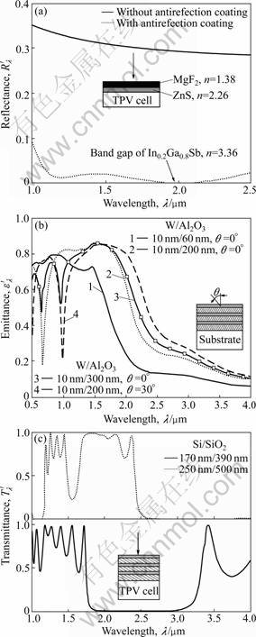
Fig.2 Normal reflectance from TPV cells with and without antireflection coatings (a), emittance of multilayer structure for wavelength-selective emitter composed of ten unit cells of tungsten/alumina films on top of tungsten substrate (b) and normal transmittance of periodic structure for wavelength- selective filter composed of five unit cells of Si/SiO2 films on top of TPV cell
Radiation sources, however, are neither perfectly coherent nor incoherent. ZHANG et al [46] used partial coherence theory to calculate the radiative properties of a layer by taking the forward propagating field in the film as being composed of two components: one is directly refracted from the incident field, and the other is the combination of multiple reflections inside the film. LEE et al [47] investigated the effects of scattering and partial coherence on the transmittance of thin films with rough surfaces. FU et al [48] used direct spectral integration to obtain analytical formulae for the reflectance and transmittance of a thin film.
4.2 Periodic gratings
The conversion efficiency of TPV systems can also be enhanced greatly by the use of micro/nanostructured gratings as wavelength-selective emitters. For the sake of simplicity, a brief discussion is provided here for s-polarized plane wave with the plane of incidence being perpendicular to the gratings, as illustrated in Fig.3(a) [31]. The wave is incident on a 1D grating surface from free space, region I with ��I=nI =1 and ��I=0. Region II is composed of binary materials A and B such that its dielectric function is a periodic function of x and ��, which is the grating period. Region III is the substrate with dielectric function ��III.
Two-dimensional metallic gratings have been extensively studied previously as emitters and filters in the TPV ystems [32,34]. But the fabrication of such the structures may not be easy. As an alternative design for the TPV emitter, 1D tungsten complex grating has been proposed [31]. Figure 3(b) shows the complex grating, which is a superposition of two simple binary gratings with different periods. The complex grating period is 1.6 ��m with four 0.2 ��m-high ridges inside. Figure 3(c) compares the spectral emittance of plain tungsten and the complex grating at emission angle �� = 0�� and 60�� for the TM wave. Compared with the plain tungsten, the complex grating has high emittance peaks within the spectral interval (0.8 ��m�ܦˡ�1.7 ��m), which corresponds to the band gap of TPV cell materials. The emittance is higher than 0.8 for 0.8 ��m�ܦˡ�1.7 ��m due to the surface plasmon polaritons and lower than 0.2 for �ˡ�2.2 ��m. Even at an emission angle of 60��, the complex grating shows higher emittance than that of plain tungsten.

Fig.3 Schematic diagram for TE wave incidence on a grating (a), tungsten complex grating with period of 1.6 ��m and ridge height of 0.2 ��m (b), comparison of spectral emittance for TM wave from complex grating and plain tungsten at ��=0�� and 60��
4.3 Near-field TPVS
To enhance the power throughput and conversion efficiency of these devices, a new type of TPV system utilizing the principle of near-field thermal radiation has been recently proposed. Placing a TPV cell in the proximity of a thermal emitter would tremendously enhance the photon energy into the cell by photon tunneling, resulting in the increase in the electric power generation. Near-field TPV system has been intensively studied by several research groups [49-52]. A near-field TPV energy conversion system consists of a TPV cell and the thermal source that are separated with a very small vacuum gap. Figure 4(a) illustrates a near-field TPV device. The thermal source is assumed to be made of tungsten and maintained at TH=2 000 K, so that the characteristic wavelength of thermal emission is 1.5 ��m. As for the TPV cell, In0.18Ga0.82Sb, an alloy of InSb and GaSb, is chosen because its energy band gap of 0.56 eV is sufficiently low for the TPV energy conversion. Figure 4(b) schematically depicts a TPV cell with a p-on-n configuration [52]. Doping concentration of the p-layer is typically set to be 1019 cm-3 whilst the tellurium-doped n-layer has a doping concentration of 1017 cm-3. The concentration gradient of the majority carriers across the p-n junction diffuses electrons from the n- to p-region and vice versa for the holes. As a result, the depletion region having only ionized dopants is formed at the junction between z=a and z=b. The depletion region width Ldp is estimated to be 0.1 ��m from the given doping concentrations. The thicknesses of the p and n-layers are 0.4 and 10 ��m, respectively. For the analysis, the TPV cell is assumed to be maintained at TC=300 K. The whole TPV system is configured with N+1 layers. The first and second layers are the semi-infinite tungsten emitter and the vacuum gap, respectively, and the last layer is the semi-infinite In0.18Ga0.82Sb substrate. The intermediate region, that is, the p-n junction part of the TPV cell, is divided into N-2 layers. Dividing the TPV cell into discrete thin layers enables to calculate the generation of electron-hole pairs due to the absorption of radiative power in each layer and the diffusion of electrons and holes to the depletion region.
Figure 5 shows the spectral distribution of the thermal radiation propagating into the TPV cell when the vacuum gap width d is set to be 10 nm [52]. The spectral power has a peak around 1.5 ��m, which is the characteristic wavelength of thermal radiation at 2 000 K. At shorter wavelengths, the net Poynting vector decays exponentially inside the cell due to the strong absorption of In0.18Ga0.82Sb. The penetration depth of the radiation inside the TPV cell increases with increasing wavelength. The radiative power at wavelengths longer than ��g�� 2.2 ��m experiences little absorption due to lattice vibrations. At ��=2.2 ��m, the penetration depth is around 5 ��m. This implies that no electron-hole pairs will be created inside the TPV cell beyond a depth of 5 ��m.
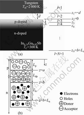
Fig.4 Schematic diagram of near-field TPV system [52] (a) and illustration of minority carrier diffusion lengths and depletion region in p-n junction (b)
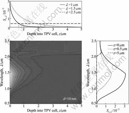
Fig.5 Spectral distribution of incident radiative power inside TPV cell at d=10 nm (Beyond ��g=2.2 ��m, there is very little absorption)
Figure 6(a) shows the total photocurrents integrated over all wavelengths as a function of the vacuum gap width. When the vacuum gap is very small, that is, d < 4 nm, Je becomes greater than Jh because a significant amount of near-field thermal radiation is absorbed very close to the surface. As mentioned earlier, at shorter vacuum gaps, the peak of the energy distribution shifts to larger �� values. Hence, the penetration depth of the incident radiation inside the TPV cell decreases as the vacuum gap is reduced. Figure 6(b) plots the conversion efficiency as a function of vacuum gap d. For comparison, the efficiency for the ideal case with 100% quantum efficiency is also plotted. Under the assumption of ��q=1, all the absorbed photons with energy greater than the band gap contribute to the photocurrent generation. Hence, the current generated in p- and n-regions are calculated without considering the diffusion and recombination. It is seen that in the ideal case, the conversion efficiency increases as the vacuum gap decreases and can reach 35% when d=2 nm. On the other hand, the conversion efficiency calculated by considering diffusion and recombination is significantly lower than the ideal case and experiences a reduction as the vacuum gap decreases below 10 nm.
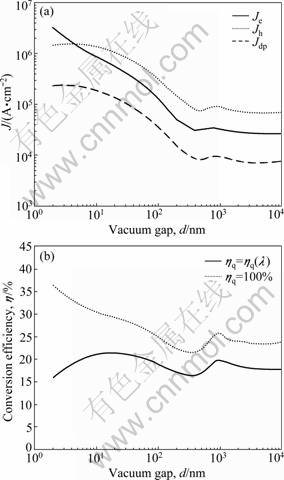
Fig.6 Effect of vacuum gap d on local current generation (a) and conversion efficiency (b) in near-field TPV systems [52]
In the near field, radiation energy transfer between two thermally emitting bodies is a strong function of the distance separating them. The spacing effect is a combined result of propagating and evanescent waves. Evanescent waves can arise due to total internal reflection when light is incident from an optically denser medium to a rarer one at angles greater than the critical angle. If another optically denser medium is brought close to the first one as shown in Fig.7(a), a backward- decaying evanescent wave is formed inside Medium 2, the optically rarer medium. It is interesting to note that, while the forward and backward evanescent waves do not carry any energy, the Poynting vector of the coupled evanescent fields has a non-zero normal component. Consequently, energy can be transmitted from the first to the third medium, even though the angle of incidence is greater than the critical angle. This phenomenon is the key for enhanced energy transfer at sub-wavelength distances and is known as radiation tunnelling, or photon tunnelling.
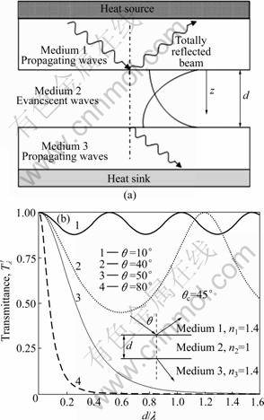
Fig.7 Illustration of evanescent waves and photon tunneling [53]: (a) Schematic drawing of three layers and field; (b) Calculated transmittance for TE wave assuming n?=n3=n2=1
Figure 7(b) shows the variation of transmittance with d/�� for thermal radiation originating from Medium 1 with refractive index n1=1.4, towards Medium 2 with n2= 1, at different angles of incidence. Since loss in the second medium is zero, the ratio of z component of the Poynting vector in Medium 2 to that in Medium 1 is the transmittance. At angles of incidence less than the critical angle (��c=45��), propagating waves exist in the second medium and interference occurs between the forward and backward propagating waves. The transmittance oscillates as the thickness of Medium 2 increases. When the angle of incidence is greater than the critical angle, evanescent waves exist in the second medium and the transmittance is a decaying function of the thickness of Medium 2.
A common way to improve the efficiency for far-field TPV system is to place a wavelength-selective filter between the emitter and TPV cell. However, filters cannot be used in the near-field TPV system because the added filter thickness may significantly diminish the near-field effects. An approach that may improve the efficiency while maintaining the near-field enhancement is depositing a thin metallic layer at the bottom of the TPV cell. This layer can serve both as an electrode and a reflector for long-wavelength photons that have a very large penetration depth. By reflecting the unusable radiation back to the emitter, the overall radiative energy transfer will decrease without reducing the photocurrent generation.
5 Conclusions
1) Several significant steps have been undertaken recently for increasing the TPV efficiency and throughput with the help of semiconductor and microfabrication technologies. On the other hand, a clear understanding of the microscale radiation, such as the enhancement of power throughput by photon tunnelling of near field, is required for the progress of TPV systems.
2) However, Some challenges still exist and need to be overcome before realizing the TPV/MTPV systems with high throughput and efficiency. First, scaling MTPV power generators with high-power throughput to macroscale TPV applications is a significant barrier. Next, the band gap of the TPV cell materials must be tailored to maximize the number of absorbed photons and to take advantage of the near-field energy enhancement. Besides, miniaturization of different TPV components results in large thermal stresses and low-dimensional tolerance. Another concern is the high cost and long fabrication time for mass production of the wavelength-selective emitters/filters. From the viewpoint of the entire MTPV system, integration of different components with electrical circuits and fuel supply loops, and effective thermal packaging is extremely challenging. Nevertheless, the growing energy demands as well as the potential applications are the driving forces to propel the development of TPV technology.
References
[1] DONALD L. Fundamentals of thermophotovoltaic energy conversion [M]. Amsterdam: Elsevier Science, 2007: 134-147.
[2] MESSENGER R A, VENTRE J. Photovoltaic systems engineering [M]. Boca Raton: CRC Press, 2004: 78-89.
[3] NELSON R E. A brief history of thermophotovoltaic development [J]. Semiconductor Science and Technology, 2003, 18(5): S141-S143.
[4] YANG W M, CHOU S K, SHU C, LI Z W, XUE H. A prototype microthermophotovoltaic power generator [J]. Applied Physics Letters, 2004, 84(19): 3864-3866.
[5] YANG W M, CHOU S K, SHU C, XUE H, LI Z W, LI D T, PAN D F. Microscale combustion research for application to micro thermophotovoltaic systems [J]. Energy Conversion Management, 2003, 44(16): 2625-2634.
[6] YANG W M, SIAWKIANG C, SHU C, XUE H, LI Z W. Effect of wall thickness of micro-combustor on the performance of micro-thermophotovoltaic power generators [J]. Sensors and Actuators, 2005, 119(2): 441-445.
[7] XUE H, YANG W M, CHOU S K, SHU C, LI Z W. Microthermophotovoltaics power system for portable MEMS devices [J]. Microscale Thermophysics Engineering, 2005, 9(1): 85-97.
[8] COUTTS T J, GUAZZONI G, LUTHER J. Thermophotovoltaic generation of electricity [C]// The Proceedings of Fifth Conference on Thermophotovoltaic Generation of Electricity. Melville: American Institute of Physics, 2003: 235-246.
[9] BIEHS S A, REDDIG D, Holthaus M. Thermal radiation and near-field energy density of thin metallic films [J]. The European Physics Journal B, 2007, 55: 237-251.
[10] FU C J, TAN W C. Near-field radiative heat transfer between two plane surfaces with one having a dielectric coating [J]. Journal of Quantitative Spectroscopy & Radiative Transfer, 2009, 110(12): 1027-1036.
[11] LAROCHE M, CARMINATI R, GREFFET J J. Near-field thermophotovoltaic energy conversion [J]. Journal of Applied Physics, 2006, 100(6): 063704-063712.
[12] MAUK M G, ANDREEV V M. GaSb-related materials for TPV cells [J]. Semiconductor Science and Technology, 2003, 18(5): S191-S201.
[13] GONZALEZ-CUEVAS J A, REFAAT T F, ABEDIN M N, ELSAYED-ALI H E. Modeling of the temperature-dependant spectral response of In1xGaxSb infrared photodetectors [J]. Optical Engineering, 2006, 45(4): 044001-044013.
[14] RADZIEMSKA E. Effect of temperature on dark current characteristics of silicon solar cells and diodes [J]. International Journal of Energy Research, 2006, 30(2): 127-134.
[15] COUTTS T J, BENNER J P. Thermophotovoltaic generation of electricity [C]// The First NREL Conference on Thermophotovoltaic Generation of Electricity. Melville: American Institute of Physics, 1994: 219-225.
[16] DINGES H W, BURKHARD H, LOSCH R, NICKEL H, SCHLAP W. Refractive indexes of InAlAs and InGaAs/InP from 250nm to 1900nm determined by spectroscopic ellipsometry [J]. Applied Surface Science, 1992, 54: 477-481.
[17] COUTTS T J, ALLMAN C S, BENNER J P. Thermophotovoltaic generation of electricity [C]// The Third NREL Conference. Melville: American Institute of Physics, 1997: 109-114.
[18] RENAUD P, RAYMOND F, BENSAID B, VERIE C. Influence of photon recycling on lifetime and diffusion-coefficient in GaAs [J]. Journal of Applied Physics, 1992, 71(4): 1907-1913.
[19] SZE S M. Physics of semiconductor devices [M]. New York: Wiley, 1981: 204-211.
[20] BENNER J P, COUTTS T J, GINLEY D S. Thermophotovoltaic generation of electricity [C]// The Second NREL Conference on Thermophotovoltaic Generation of Electricity. Melville, American Institute of Physics, 1995: 201-212.
[21] FAHRENBRUCH A L, BUBE R H. Fundamentals of solar cells: Photovoltaic solar energy conversion [M]. New York: Academic Press, 1983: 156-159.
[22] GREE M A. Solar cells: Operating principles, technology, and system applications [M]. NJ: Prentice-Hall, 1982: 543-549.
[23] ZENKER M, HEINZEL A, STOLLWRECK G, FERBER J, LUTHER J. Efficiency and power density potential of combustion driven thermophotovoltaic systems using GaSb photovoltaic cells [J]. IEEE Electronic Devices, 2001, 48(2): 367-376.
[24] BALDASARO P F, RAYNOLDS J E, CHARACHE G W, DEPOY D M,BALLINGER C T, DONOVAN T, BORREGO J M. Thermodynamic analysis of thermophotovoltaic efficiency and power density tradeoffs [J]. Journal of Applied Physics, 2001, 89(6): 3319-3327.
[25] DEMICHELIS F, MINETTIMEZZETTI E, AGNELLO M, TRESSO E. Evaluation of thermophotovoltaic conversion efficiency [J]. Journal of Applied Physics, 1982, 53(12): 9098-9104.
[26] MAHORTER R G, WERNSMAN B, THOMAS R M, SIERGIEJ R R. Thermophotovoltaic system testing [J]. Semiconductor Science and Technology, 2003,18(5): S232-S238.
[27] LICCIULLI A, DISO D, TORSELLO G, TUNDO S, MAFFEZZOLI A, LOMASCOLO M, MAZZER M. The challenge of high performance selective emitters for thermophotovoltaic applications [J]. Semiconductor Science and Technology, 2003, 18(5): S174-S183.
[28] TORSELLO G, LOMASCOLO M, LICCIULLI A, DISO D, TUNDO S, MAZZER M. The origin of highly efficient selective emission in rare-earth oxides for thermophotovoltaic applications [J]. Nature Materials, 2004, 3(9): 632-637.
[29] CHUBB D L, WOLFORD D S. Dual layer selective emitter [J]. Applied Physics Letters, 2005, 87(14): 141907-141912.
[30] NARAYANASWAMY A, CHEN G. Thermal emission control with one-dimensional metallodielectric photonic crystals [J]. Physics Review B, 2004, 70(12): 125101-125109.
[31] CHEN Y B, ZHANG Z M. Design of tungsten complex gratings for thermophotovoltaic radiators [J]. Optical Communications, 2006, 269: 411-417.
[32] HEINZEL A, BOERNER V, GOMBERT A, BLASI B, WITTWER V, LUTHER J. Radiation filters and emitters for the NIR based on periodically structured metal surfaces [J]. Journal of Modern Optics, 2000, 47(13): 2399-2419.
[33] SAI H, KANAMORI Y, YUGAMI H. High-temperature resistive surface grating for spectral control of thermal radiation [J]. Applied Physics Letters, 2003, 82(11): 1685-1687.
[34] SAI H, KANAMORI Y, YUGAMI H. Tuning of the thermal radiation spectrum in the near-infrared region by metallic surface microstructures [J]. Journal of Micromechanics and Microenergy, 2005, 15(9): S243-S249.
[35] BAUER T, FORBES I, PENLINGTON R, PEARSALL N. Heat transfer modeling in the thermophotovoltaic cavities using glass media [J]. Solar Energy Materials and Solar Cells, 2005, 88: 257-268.
[36] FRAAS L M, AVERY J E, HUANG H X, MARTINELLI R U. Thermophotovoltaic system configurations and spectral control[J]. Semiconductor Science and Technology, 2003, 18(5): S165-S173.
[37] KIZILTAS G, VOLAKIS J L, KIKUCHI N. Design of a frequency selective structure with inhomogeneous substrates as a thermophotovoltaic filter [J]. IEEE T Antennas and Propagation, 2005, 53(7): 2282-2289.
[38] VIGIL O, RUIZ C M, SEURET D, BERMUDEZ V, DIEGUEZ E. Transparent conducting oxides as selective filters in thermophotovoltaic devices [J]. Journal of Physics: Condensed Matter, 2005, 17(41): 6377-6384.
[39] CELANOVIC I, O��SULLIVAN F, ILAK M, KASSAKIAN J, PERREAULT D. Design and optimization of one-dimensional photonic crystals for thermophotovoltaic applications [J]. Optics Letter, 2004, 29(8): 863-865.
[40] O��SULLIVAN F, CELANOVIC I, JOVANOVIC N, KASSAKIAN J. Optical characteristics of one-dimensional Si/SiO2 photonic crystals for thermophotovoltaic applications [J]. Journal of Applied Physics, 2005, 97(3): 033529-033537.
[41] FOURSPRING P M, DEPOY D M, RAHMLOW T D, LAZO-WASEM J E, GRATRIX E J. Optical coatings for thermophotovoltaic spectral control [J]. Applied Optics, 2006, 45(7): 1356-1358.
[42] GOPINATH A, COUTTS T J, LUTHER J. Thermophotovoltaic generation of electricity [C]// The Sixth Conference on Thermophotovoltaic Generation of Electricity. Melville: American Institute of Physics, 2004: 231-240.
[43] COCKERAM B V, MEASURES D P, MUELLER A J. The development and testing of emissivity enhancement coatings for thermophotovoltaic (TPV) radiator applications [J]. Thin Solid Films, 1999, 356: 17-25.
[44] CHUBB D L, WOLFORD D S. Dual layer selective emitter [J]. Applied Physics Letters, 2005, 87(14): 141907-141916.
[45] MARTIN P M, OLSEN L C, JOHNSTON J W, DEPOY D M. Investigation of sputtered HfF4 films and application to interference filters for thermophotovoltaics [J]. Thin Solid Films, 2002, 420: 8-12.
[46] ZHANG Z M, FU C J, ZHU Q Z. Optical and thermal radiative properties of semiconductors related to micro/nanotechnology [J]. Advanced Heat Transfer, 2003, 37: 179-296.
[47] LEE B J, KHUU V P, ZHANG Z M. Partially coherent spectral radiative properties of dielectric thin films with rough surfaces [J]. Journal of Thermophysics Heat Transfer, 2005, 19: 360-366.
[48] FU K, HSU P F, ZHANG Z M. Unified analytical formulation of thin-film radiative properties including partial coherence [J]. Applied Optics, 2006, 45(4): 653-661.
[49] WHALE M D, CRAVALHO E G.. Modeling and performance of microscale thermophotovoltaic energy conversion devices [J]. IEEE Transactions on Energy Conversion, 2002, 17(1): 130-142.
[50] NARAYANASWAMY A, CHEN G. Surface modes for near field thermophotovoltaics [J]. Applied Physics Letters, 2003, 82(20): 3544-3546.
[51] LAROCHE M, CARMINATI R, GREFFET J J. Near-field thermo-photovoltaic energy conversion [J]. Journal of Applied Physics, 2006, 100(6): 063704-063711.
[52] PARK K, KING W P. Performance analysis of near-field thermophotovoltaic devices considering absorption distribution [J]. Journal of Quantitative Spectroscopy and Radiative Transfer, 2008, 109(2): 305-316.
[53] BSU S, ZHANG Z M. Maximum energy transfer in near-field thermal radiation at nanometer distances [J]. Journal of Applied Physics, 2009, 105(9): 09353-09360.
(Edited by YANG Bing)
Foundation item: Project(2009AA05Z215) supported by the National High Technology Research and Development Program of China
Received date: 2011-01-11; Accepted date: 2011-05-26
Corresponding author: WANG Ai-hua, PhD; Tel: +86-13624210542; E-mail: wangaihua1976@yahoo.com.cn
Abstract: Thermophotovoltaic (TPV) system has been regarded as one promising means to alleviate current energy demand because it can directly generate electricity from radiation heat via photons. However, the presently available TPV systems suffer from low conversion efficiency and low throughput. A viable solution to increase their efficiency is to apply micro/nanoscale radiation principles in the design of different components to utilize the characteristics of thermal radiation at small distances and in microstructures. Several critical issues are reviewed, such as photovoltaic effect, quantum efficiency and efficiency of TPV system. Emphasis is given to the development of wavelength-selective emitters and filters and the aspects of micro/nanoscale heat transfer. Recent progress, along with the challenges and opportunities for future development of TPV systems are also outlined.
