

Precipitation and gettering behaviors of copper in multicrystalline silicon used for solar cells
LI Xiao-qiang, YANG De-ren, YU Xue-gong, QUE Duan-lin
State Key Laboratory of Silicon Materials, Department of Materials Science and Engineering,
Zhejiang University, Hangzhou 310027, China
Received 22 October 2010; accepted 1 December 2010
Abstract:
The precipitation and gettering behaviors of copper (Cu) at different defective regions in multicrystalline silicon were investigated by combining scanning infrared microscopy, optical microscopy, inductively coupled plasma mass spectrometry and microwave photo-conductance decay. It is found that the behaviors of Cu precipitation are strongly dependent on the defect density. Most of the Cu contaminants tend to form precipitates homogeneously in the low density defect region, while they mostly segregate at the defects and form precipitates heterogeneously in the high density defect region. In the case of heavy contamination, the Cu precipitate can significantly reduce the carrier lifetime of multicrystalline silicon due to their Schottkydiode behavior in the silicon substrate. A 900 ��C rap thermal process (RTP) phosphorus gettering anneal cannot be sufficiently effective to remove the Cu precipitates in these two regions.
Key words:
multicrystalline silicon; Cu precipitate; phosphorus gettering; defects; carrier lifetime;
1 Introduction
Since the solar cells are moving towards high efficiency and low cost, more and more attention has been paid to the multicrystalline silicon (mc-Si) materials. Because of the grown-in defects, the electrical properties of mc-Si are not as good as those of single crystalline silicon, especially in the case of metal contamination[1-2]. It has been known that metal impurity decoration can increase the recombination activity of defects, including grain boundaries and dislocations[3-4]. Furthermore, in recent years, the use of low quality raw materials increases the risk of metal contamination[5-7].
Copper (Cu) is one of the most common transition metal impurities in silicon materials and solar cells[8], which can be easily introduced during the fabrication of wafers and devices. It could introduce deep levels and a series of extended defects into silicon[9], degrading the electrical properties of solar cells. Cu favors to form precipitates in the silicon bulk, due to its fast diffusivity and low solubility at room temperature. The behaviors of copper precipitation in single crystalline silicon have been studied for decades[10-12], and many basic properties have been obtained[13-15]. However, for mc-Si, the involvement of defects will make the behaviors of Cu precipitation more complicated. A clear understanding on the effect of defects on the Cu precipitation in mc-Si is still needed.
In this work, the influence of the defect density on the precipitation and the gettering behaviors of the Cu precipitates with different forms was investigated to enhance our understanding of the interaction between Cu impurities and defects in photovoltaic multicrystalline silicon.
2 Experimental
Samples used in this study were cut from a p-type mc-Si ingot. The resistivity of these samples is about 1 ��?cm. These samples were especially selected and had two distinct regions with various defect densities, as shown by the optical micrographs (OMs) in Fig.1. The low density defect region contains dislocations with a density lower than 104 cm-2. The high density defect region contains the dislocations in the order of 105 cm-2, and the grain boundaries with a density higher than low ensity defect region. Firstly, the samples were chemically polished in a mixture of HNO3 and HF (v(HNO3):v(HF)=1:3) to remove the damage layer. The concentration of substitutional carbon in the samples was about 3��1017 cm-3 and interstitial oxygen was about 2��1017 cm-3, measured by a Bruker IFS 66 V/S Fourier transform infrared spectroscope (FTIR) with a calibration coefficient of 1��1017 cm-2 and 3.14��1017 cm-2 for carbon and oxygen, respectively. After standard RCA and HF cleaning, the samples were intentionally subjected to Cu contamination by dipping the samples into 0.5 mol/L CuCl2 solution, pre-drying at 100 ��C and then in-diffusing by annealing at selected temperatures. The Cu remnants on the sample surfaces were removed by chemical mechanical polishing. The carrier lifetime after Cu contamination was measured by microwave photo-conductance decay (MW-PCD) technique with iodine-methanol solution passivation (0.1 mol/L). Then, the copper precipitate geometries were studied using scanning infrared microscopy (SIRM) and optical microscopy techniques (OM) after Secco etching.
For phosphorus gettering, the liquid phosphorus resource (p-854, Honeywell) was spun on one side of the samples, followed by pre-baking at 200 ��C for 10 min. The phosphorus in-diffusion treatments were performed by a rap thermal process (RTP) annealing at 900 ��C for 60 s with argon protection. The cooling rate for the
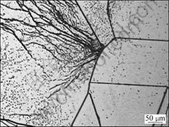
Fig.1 OM micrograph of as-grown sample containing two different density defect regions after Secco etching
gettering process was about 30 K/s. Phosphorus glass layers were removed by a diluted HF solution. The copper concentrations in these two regions before and after gettering were measured by inductively coupled plasma mass spectrometry technique (ICP-MS, Thermo Scientific Xeries II).
3 Results and discussion
3.1 Behavior of Cu precipitation in low density defect region
Fig.2 shows the SIRM images of precipitates
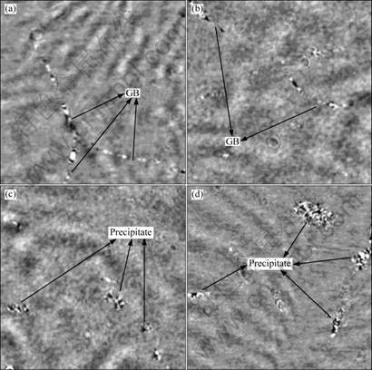
Fig.2 SIRM images of precipitates in low density defect region related to Cu impurity contaminated at different temperatures: (a) 600 ��C; (b) 900 ��C; (c) 1 000 ��C; (d) 1 200 ��C
geometries in the low density related to Cu impurity defect region contaminated at 600-1 200 ��C. It can been seen that, when contaminated at 600 ��C, no obvious Cu precipitates but the grain-boundaries (GBs) and dislocations with very weak contrast are observable (Fig.2(a)). In the case of Cu contamination at 900 ��C, the phenomenon is nearly the same, GBs and dislocations become broader (Fig.2(b)), which means that more Cu impurities have segregated at the sites of these defects. After contamination at 1 000 ��C, a number of Cu precipitate colonies can also be seen in the bulk besides GB sites (Fig.2(c)). Similar to the case of being contaminated at 1 000 ��C, when contamination temperature is 1 200 ��C, the colony-like Cu precipitate with even larger size and higher density can be seen in the bulk. These Cu precipitates should be formed based on the homogeneous nucleation.
MW-PCD can be used to investigate the recombination activity of Cu in mc-Si samples contaminated at different temperatures. A carrier lifetime ��Cu related to Cu contamination is defined by
![]() (1)
(1)
where ��as-grown is the as-grown effective lifetime of the mc-Si sample; ��con is the effective lifetime after Cu contamination. 1/��Cu can be understood as the normalized density of Cu-related recombination centers. The relationship between 1/��Cu and contamination temperatures is shown in Fig.3. It can be seen that when contaminated below 900 ��C, the recombination activity of Cu-related centers in mc-Si is relatively low, while the recombination activity increases with increasing the contamination temperature, as shown in the inset. When contaminated above 900 ��C, the recombination activity of Cu-related centers increases with a greater pace with the increase of contamination temperature. The high Cu recombination activity can be attributed to the formation of Cu precipitates in the inner-grain region, as shown SIRM measurements results above. The density of the Cu precipitates formed in the inner-grain region can be obtained from the SIRM measurements, which are about 4.3��104 cm-2 and 5.4��104 cm-2 in the cases of Cu contamination at 1 000 ��C and 1 200 ��C, respectively. It is believed that the recombination activity of Cu precipitates in silicon arises from the interface of the precipitate and the Si bulk, which behaviors like a metal/silicon Schottky diode. The minority carrier recombination velocity at this interface could be infinite. The Cu precipitates formed at 1 200 ��C have larger size and higher density than those formed at 1 000 ��C, and therefore introduce larger interfaces into Si bulk than smaller ones. So, Cu precipitates in the sample conta- minated at 1 200 ��C have much higher recombination activity than those in sample contaminated at 1 000 ��C.

Fig.3 Normalized concentration of Cu-related recombination centers in low density defect region contaminated at different temperatures
3.2 Behavior of Cu precipitation in high density defect region
Fig.4 shows the OM micrographs in the high density defect region with Cu contamination after Secco etching. In the case of Cu contamination at 700 ��C, as can be seen in Fig.4(a), except for the defects etching pits, no precipitate etching geometries can be obviously observed. When contaminated at 1 000 ��C, the preferential etching morphology is similar, few precipitates etching morphologies can be found. We have measured the Cu concentration in this region after contamination at 1 000 ��C using ICP-MS. The results reveal that the concentration of Cu in this region is in the magnitude of 1016 cm-3. However, we cannot find any precipitates after etching, so we believe that the Cu atoms introduced by thermal annealing mainly decorate on defects. After being contaminated at 1 200 ��C, a few precipitate-induced morphologies can be found in this region besides the etching pits arisen from defects.
Accordingly, 1/��Cu is again used here to evaluate the recombination activity of Cu-related centers in the high density defect region, which is shown in Fig.5. One can see that the normalized concentration of Cu-related recombination centers increases with an increase of the contamination temperature. Unlike those in the low density defect region, Cu-related centers already have quite great effect on the carrier lifetime in the case of a relatively low temperature contamination, e.g. 800 ��C. Also, we can find that the normalized concentration of Cu-related centers increases more rapidly by a higher temperature contamination. This can be explained by the forms of Cu impurities existing at defects. In the case of low temperature contamination, Cu impurities interacting with the defects stay at the defect cores. This will increase the recombination activity of defects to some degree. However, in the case of high temperature contamination, these Cu impurities gettered at the defects
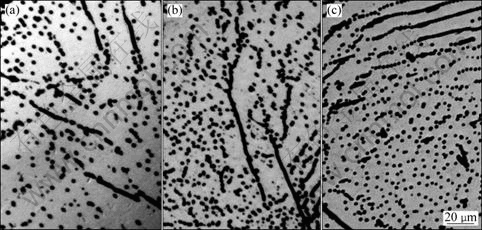
Fig.4 OM micrographs of high density defect region after Cu contamination at different temperatures: (a) 700 ��C; (b) 1 000 ��C; (c) 1 200 ��C
tend to form large precipitates. As mentioned before, these large Cu precipitates can cause Schottky barrier in the substrate. Therefore, it is believed that there exists an infinite recombination velocity at the precipitate/silicon interface, resulting in that the normalized concentration of Cu-related recombination centers drastically increases.
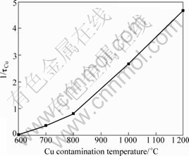
Fig.5 Normalized concentration of Cu-related recombination centers in high density defect region contaminated at different temperatures
3.3 Formation mechanisms of two different Cu precipitates
It has been reported that there is a critical concentration for Cu to form precipitates homogeneously in silicon. Below this critical concentration, if there is no gettering sites, e.g. defects, Cu atoms will mainly out-diffuse to the surfaces, while above this critical contamination level, precipitates tend to form in the bulk[16]. In mc-Si, the defects including GBs and dislocations can serve as segregation sites for Cu impurities[17]. At low contamination temperatures, the concentration of introduced Cu is below the critical level, and no precipitates can be formed homogeneously. All the Cu impurities remained in the bulk will segregate at the defects. The behaviors of Cu precipitation in the regions with different density defects are basically the same. A high density defects can capture more Cu staying in the bulk, thus leading to higher density of Cu-related recombination centers. However, at high contamination temperatures, two competitive processes of Cu precipitation could happen. In the high concentration region of Cu impurities, precipitates could form either by homogeneous nucleation or by heterogeneous nucleation at defects. In the low density defect regions, the homogeneous nucleation is dominant, and therefore, high density of Cu precipitates can be formed in the inner-grain regions. In the high density defect region, Cu precipitates mostly nucleate at the defects and fewer precipitates can form in the inner-grain region.
3.4 Cu phosphorus gettering in mc-Si
Fig.6 shows the Cu concentration in the regions with high defect density and low defect density before and after a 900 ��C RTP phosphorus gettering. The sample is heavily Cu-contaminated since the Cu contamination temperature is 1 000 ��C. The Cu concentrations in the regions with different defect densities are all about 1017 cm-3. After RTP gettering, Cu concentrations in these two regions are both decreased. In high defect density region, the Cu concentration decreases from 8.1��1016 cm-3 to 6.7��1016 cm-3, i.e., only 17% of Cu impurities have been gettered out. In a low density defect region, the Cu concentration decreases from 10.4��1016 cm-3 to 7.2��1016 cm-3, i.e., about 35% of Cu impurities have been gettered out. It is obvious that the reduction of Cu contaminants in low density defect region is larger than that in high density defect region.
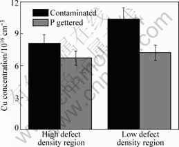
Fig.6 Cu concentrations in two different density defect regions before and after RTP phosphorus gettering
However, it should be noted that the concentration of the remained Cu impurities in low density defect region is still slightly larger than that in the high density defect region after RTP phosphorus gettering. It has been reported that together with the formation of Cu precipitates, dislocation loops will be punched out by the ejection of Si interstitial atoms due to the volume expanding[18]. Thus, colony-type Cu precipitates actually consist of a group of dislocations and precipitates. Dissolution of this type of Cu precipitates by RTP have been studied in CZ Si previously[19], it was found that complete dissolution of these precipitates is very hard. So, after RTP phosphorus gettering, a large portion of Cu impurities still remain in the low density defect region. In the high density defect region, Cu phosphorus gettering is limited to the competition between high density defects and the phosphorus diffused layer. These results suggest that the RTP phosphorus gettering at 900 ��C is not so effective for gettering of both the large-size Cu precipitates in the inner-grains and those decorate at the structural defects.
4 Conclusions
1) In the low density defect region in mc-Si, Cu impurities mostly diffuse out of the sample in the case of low contamination level. With a high contamination level, the Cu impurities tend to form precipitates homogeneously in the inner-grain region, and therefore larger sized Cu precipitates are observed. The Cu precipitates can significantly reduce the carrier lifetime in this region due to their strong recombination activity.
2) At the high density defect region in mc-Si, Cu contaminants mostly are gettered by the defects. They will form precipitates heterogeneously. These Cu precipitates have a large density and increase the recombination activity of defects and therefore also degrade the carrier lifetime significantly.
3) Since the Cu precipitates exist as colony-like, the punched-out dislocation loops interacting with the precipitates increase the thermal stability of Cu precipitates. By a 900 ��C RTP phosphorus gettering, the Cu precipitates in both regions cannot significantly be effectively removed. So, the carrier lifetime of the sample cannot be improved largely.
References
[1] Elghitani H, Martinuzzi S. Influence of dislocations on electrical-properties of large grained polycrystalline silicon cells: 2. Experimental results [J]. Journal of Applied Physics, 1989, 66(4): 1723-1726.
[2] Chen J, Sekiguchi T, Yang D, Yin F, Kido K, Tsurekawa S. Electron-beam-induced current study of grain boundaries in multicrystalline silicon [J]. Journal of Applied Physics, 2004, 96(10): 5490-5495.
[3] Kveder V, Kittler M, Schroter W. Recombination activity of contaminated dislocations in silicon: A electron-beam-induced current contrast behavior [J]. Physical Review B, 2001, 63(11): 115208-115211.
[4] Chen B, Chen J, Sekiguchi T, Saito M, Kimoto K, Structural characterization and iron detection at Sigma 3 grain boundaries in multicrystalline silicon [J]. Journal of Applied Physics, 2009, 105(11): 113502.
[5] LONG Gui-hua, WU Bin, HAN Song, QIU Ke-qiang. Development status and prospect of solar grade silicon production technology [J]. The Chinese Journal of Nonferrous Metals, 2008, 18(s1): s386-392. (in Chinese)
[6] Degoulange J, P��richaud I, Trassy C, Martinuzzi S. Multicrystalline silicon wafers prepared from upgraded metallurgical feedstock [J]. Solar Energy Materials and Solar Cells, 2008, 92(10): 1269-1273.
[7] Martinuzzi S, Perichaud I, Trassy C, Degoulange J. n-type multicrystalline silicon wafers prepared from plasma torch refined upgraded metallurgical feedstock [J]. Progress in Photovoltaics, 2009, 17(5): 297-305.
[8] Buonassisi T, Vyvenko O F, Istratov A A, Weber E R, Hahn G, Sontag D, Rakotoniaina J P, Breitenstein O, Isenberg J, Schindler R. Assessing the role of transition metals in shunting mechanisms using synchrotron-based techniques [C]//Proceedings of 3rd World Conference on Photovoltaic Energy Conversion. Osaka, 2003: 1120-1123.
[9] Knack S. Copper-related defects in silicon [J]. Materials Science in Semiconductor Processing, 2004, 7(3): 125-141.
[10] Flink C, Feick H, McHugo S A, Seifert W, Hieslmair H, Heiser T, Istratov A A, Weber E R. Out-diffusion and precipitation of copper in silicon: An electrostatic model [J]. Physical Review Letters, 2000, 85(23): 4900-4903.
[11] CHEN J, YANG D R, XI Z Q, QUE D L, SEKIGUSHI T. Electron beam induced current investigation of copper precipitates in multicrystalline silicon [J]. Acta Energiae Solaris Sinica, 2005, 26(1): 1-5.
[12] Seibt M, Graff K. Characterization of haze-forming precipitates in silicon [J]. Journal of Applied Physics, 1988, 63(9): 4444-4450.
[13] Hall R N, Racette J H. Diffusion and solubility of copper in extrinsic and intrinsic germanium, silicon, and gallium arsenide [J]. Journal of Applied Physics, 1964, 35(2): 379-397.
[14] Chen y w, hao q y, lIU c c, zHAO j g, WU d, wANG y. Effect of transition-metal contamination on minority lifetime of cast multi-crystalline silicon under rapid thermal processing [J]. Acta Engergiae Solaris Sinica, 2009, 30(5): 611-614.
[15] Istratov A A, Weber E R. Physics of copper in silicon [J]. Journal of the Electrochemical Society, 2002, 149(1): G21-G30.
[16] Flink C, Feick H, McHugo S A, Mohammed A, Seifert W, Hieslmair H, Heiser T, Istratov A A, Weber E R. Formation of copper precipitates in silicon [J]. Physica B, 1999, 273-274: 437-440.
[17] Li X, Yang D, Yu X, Que D. Copper precipitates in multicrystalline silicon for solar cells [J]. ECS Transactions, 2010, 27(1): 1135-1140.
[18] Wang W, Yang D, Ma X, Que D. Effect of silicon interstitials on Cu precipitation in n-type Czochralski silicon [J]. Journal of Applied Physics, 2008, 103(9): 093534.
[19] Sparks D R. Dissolution of transition metal precipitates in silicon by rapid thermal processing [J]. Journal of the Electrochemical Society, 1987, 134(2): 458-462.
ͭ������̫������öྦྷ���еij�����������Ϊ
����ǿ������ʣ���ѧ�����ڶ���
�㽭��ѧ ���Ͽ�ѧ�빤��ѧϵ������Ϲ����ص�ʵ���ң����� 310027
ժ Ҫ������ɨ�������������ѧ�����������ϵ����������Ǻ�����絼˥���Ƕ�ͭ�����ڶྦྷ���в�ͬȱ��״̬����ij�����������Ϊ�����о�������ͭ���ʳ�����Ϊ��ȱ���ܶ�������أ��ڵ�ȱ���ܶ�����ͭ���ʴ�����ھ����κ��γɳ��������ڸ�ȱ���ܶ�����ͭ����ͨ����ۼ���ȱ�ݴ������κ˶�������������ͭմ�����ϸ�ʱ�������ڹ�����е�Ф�ػ�������ЧӦ��ͭ��������ྦྷ���е������������������̡���900 ���½��п��������Ӵ����������������е�ͭ���ʶ����ܵõ���Чȥ����
�ؼ��ʣ��ྦྷ�裻ͭ���ʣ������ӣ�ȱ�ݣ�����������
(Edited by YANG Hua)
Foundation item: Projects (60906002, 50832006) supported by the National Natural Science Foundation of China; Project (2009QNA4007) supported by the Fundamental Research Funds for the Central Universities, China
Corresponding author: YU Xue-gong; Tel: +86-571-87953003; E-mail: yuxuegong@zju.edu.cn
DOI: 10.1016/S1003-6326(11)60767-X
