
Trans. Nonferrous Met. Soc. China 27(2017) 1199-1205
Growth behavior and microstructure of intermetallics at interface of AuSn20 solder and metalized-Ni layer
Xiao-feng WEI1, Xue-wei ZHU1, Ri-chu WANG2
1. College of Mechanical and Electronic Engineering, Northwest A&F University, Yangling 712100, China;
2. School of Materials Science and Engineering, Central South University, Changsha 410083, China
Received 28 April 2016; accepted 30 December 2016
Abstract:
The AuSn20/Ni joints were prepared by the reflow soldering technology and then annealed at solid-state temperature to form diffusion couples. The interfacial reactions and the growth kinetics of the intermetallic compounds (IMC) at the AuSn20/Ni soldering interface were investigated by scanning electron microscopy (SEM) and electron probe microanalysis (EPMA). The results show that, the (Ni,Au)3Sn2 phases are formed at the AuSn20/Ni interface after soldering at 583 K. The thickness l of the IMC layer monotonically increases with increasing annealing time t according to the relationship l=k(t/t0)n, where the exponent n is 0.527, 0.476 and 0.471 for 393, 433 and 473 K annealing, respectively. This indicates that the volume diffusion contributes to the growth of the IMC layer at the AuSn20/Ni interface at solid-sate temperature. The pre-exponential factor K0=1.23��10-7 m2/s and the activation enthalpy QK=81.8 kJ/mol are obtained from the results of the parabolic coefficient K by a least-squares method.
Key words:
AuSn20/Ni joint; interfacial reaction; growth kinetics; volume diffusion mechanism;
1 Introduction
The AuSn20 (mass fraction, %) alloy is broadly used in the bonding applications in microelectronic and optoelectronic packages, i.e., chip attach, ceramic insulators in metal packages and high power semiconductor laser chip, because of its advantages in high strength, low elastic modulus, high thermal conductivity, excellent fatigue and creep resistance, good corrosion resistance and weld ability [1-4]. Furthermore, the AuSn20 solder can be applied through a fluxless bonding process [5]. Copper is widely used in the under bump metallurgy and substrate metallization for flip-chip and ball grid array (BGA) applications. However, at the Cu/solder interface, Sn reacts rapidly with Cu and forms Cu-Sn intermetallic compounds (IMC), which weakens the solder joints due to the brittle nature of the IMC [6]. Consequently, Ni is commonly used to provide a diffusion barrier between Cu components and Sn or Sn-based solder alloys to prevent, or at least suppress, the formation of Cu-Sn intermetallic compounds. Besides, Ni has good wetting characteristics with Sn. It is an effective additive with stable phases, formed in the Ni-Sn binary system, whose growth rate is slower than those of Cu intermetallic compounds [7]. Further study on the reactive interface between the Au-Sn solder and Ni is required for electronic packaging applications.
The solid-state reactive diffusion of Au-Ni-Sn ternary system was experimentally observed sandwich diffusion couples by a diffusion bonding technique in previous studies [8,9]. For the Au-Ni/Sn system [8], sandwich Sn/Au-Ni/Sn diffusion couples with various Ni contents were isothermally annealed at T=433, 453 and 473 K for different time. Here, the notation (A-B)/C means that reactive diffusion occurs between a binary A-B alloy and a pure C metal at appropriate annealing temperatures. At the Au-20Ni/Sn interface Au1.5Ni0.5Sn8 and AuNi2Sn4 compound layers are found, and the exponent n of the power function for the IMC layer is close to 0.5 at T=453-473 K, and is 0.7 at T=433 K, while at the Au-10Ni/Sn interface, Au1.7Ni0.3Sn8, AuSn2 and Au6Ni4Sn15 compound layers are dispersed and fine particles of AuNi2Sn4 are observed, n is smaller than 0.5 at T=453-473 K, but close to 0.5 at T=433 K. This claims that the growth behavior of the IMC layer in the Au-Ni/Sn system depends on the alloyed types and components in the diffusion couples. On the other hand, the solid-state reactive diffusion in the ternary Sn-Ni/Au system was experimentally observed using Sn-Ni/Au/ Sn-Ni diffusion couples by MITA [9]. In that experiment, binary Sn-Ni alloys containing 1%, 3% and 5% of Ni were used to prepare the diffusion couples by diffusion bonding technique. The diffusion couples were isothermally annealed at 433-473 K. During annealing, AuNiSn8, AuSn4, AuSn2 and AuSn layers are formed at the Sn-Ni/Au interface, and the values of n are smaller than 0.5. This indicates that both grain boundary diffusion and volume diffusion contribute to the rate-controlling growth processes of the compound layers and the grains in the compound layers.
So far, the AuSn20 solder has been widely used in the electronic packaging, but the growth behavior of the IMC layers between Au-Sn alloy and Ni is still unclear enough. To investigate the kinetic features of the interfacial reaction, solid-state reactive diffusion in the ternary Au-Sn/Ni system was studied in the present work. AuSn20/Ni soldering joints diffusion couples were prepared from metalized-Ni layer and binary Au-Sn alloyed solder by soldering technique and diffusion bonding, and then isothermally annealed at 393-473 K for various time. The growth behavior of IMC layers was observed metallographically. The rate-controlling process for the growth of the IMC layers was further discussed.
2 Experimental
The Au-Sn solder was prepared by laminate-rolling and alloy-annealing process in this work. Firstly, polycrystalline pure Sn chips with dimensions of 10 mm �� 5 mm �� 0.1 mm were cut from a commercial rectangular ingot with purity of 99.99%. Polycrystalline pure Au chips with dimensions of 10 mm �� 5 mm �� 0.4 mm were cut from a commercial rectangular bar with purity of 99.999%. After cleaning, the Au sheet specimens were immediately folded with the freshly prepared Sn plate specimens at the sequence of Au/Sn/Au/Sn/Au/Sn/Au and then cold rolled to form a mixed metal with thickness of 0.06 mm, further alloyed annealing at 493 K for 12 h. Figure 1 presents the cross-sectional scanning electron microscopy (SEM) image of the rolled-state and alloyed AuSn20 solder used in this work. The AuSn20 solder was cut into small pieces with dimensions of 10 mm �� 5 mm �� 0.06 mm.
The Cu plates were metalized with Ni by the electroplating in the NiSO4 solution. The metalized Ni layer is about 6 ��m. After chemical polishing, the sheet AuSn20 solder was immediately used to form AuSn20/Ni soldering joints with metalized Cu plates. The schematic illustration of the configuration is shown in Fig. 2. The soldering specimens were reflowed in a reflow machine with a maximum temperature of 583 K for 60 s, and then cooled to room temperature in oil. Following the soldering process, some of the specimens were retained in an as-solidified condition, while the others were further thermally annealed at 393, 433 and 473 K for various time.
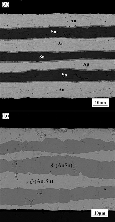
Fig. 1 Cross-sectional images of rolled (a) and alloyed (b) AuSn20 solder
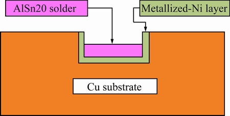
Fig. 2 Schematic illustration of soldering configuration
Common metallographic practices were used to prepare the samples for cross-section images of the reflowed and the annealed samples. The back-scattered electron image (BEI) of the microstructure was observed by scanning electron microscope (SEM). Concentration profiles of Au, Ni and Sn were measured on the cross-section along the direction normal to the Au-Sn/Ni interface by electron probe microanalysis (EPMA). The thickness of the IMC layer was calculated by the Image-pro plus (IPP) professional image analysis software.
3 Results and discussion
3.1 Microstructure of as-solidified joint
The typical cross-sectional BEI image of the as-solidified joint is shown in Fig. 3. The microstructure of the solder matrix is composed of dark (Au,Ni)Sn and bright (Au,Ni)5Sn phases. These compounds have the ��-(AuSn) and ��-(Au5Sn) crystal structures, respectively, but have small amounts of Ni dissolved in the Au sublattice. Only one irregular-shaped reaction product is found between the Au-Sn solder and the Ni layer after reflow. The composition of the reaction product is 15.42%Au-43.19%Ni-41.39%Sn (mole fraction) according to the EPMA measurements. The mole ratio of the (Au+Ni) to that of Sn is (15.42+43.19):(41.39), which is close to 3:2. This suggests that the reaction product is the (Au,Ni)3Sn2 IMC, with Ni3Sn2 phase crystal structure.
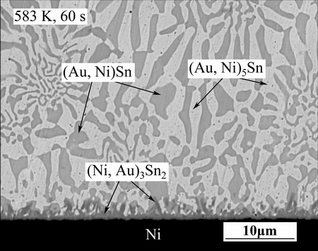
Fig. 3 SEM image of as-solidified AuSn20/Ni joint
As to the Au-Ni-Sn system, the formation enthalpy of Ni3Sn2, AuSn and Au5Sn is -31.3, -15.4 and -5.8 kJ/mol [10-12], respectively. This indicates that Ni3Sn2 phase is a stable phase formed during solidification. On the other hand, some binary phases such as AuSn, Au5Sn, Ni3Sn4 and Ni3Sn2 in the Au-Ni-Sn system have a very high solubility of the third element, due to the similarity in the chemical and physical properties of Au and Ni [13]. It seems that Ni enters into ��-(AuSn) and ��-(Au5Sn) lattice and substitutes Au atoms, while the Au enters into the Ni3Sn2 lattice and substitutes Ni atoms. A ternary IMC often has a lower Gibbs free energy than a binary compound of the same structure from the entropy argument [14]. Therefore, ��-(AuSn), ��-(Au5Sn) and Ni3Sn2 have a natural tendency to absorb Ni or Au to reach its saturated composition. This finding is consistent with the results reported by previous investigators [7,15,16].
The average thickness of the (Au,Ni)3Sn2 IMC layer formed at the interface is approximately 0.4 ��m. Above the thin (Au,Ni)3Sn2 layer, some rod-shape (Au,Ni)3Sn2 phases are found. The EPMA analysis location of the rop-shape (Au,Ni)3Sn2 is denoted as red cross in Fig. 3, and the composition is 17.11%Au-42.34%Ni-40.55%Sn (mole fraction). The rod-shape (Au,Ni)3Sn2 phase has a higher Au content, as compared to the interfacial thin (Au,Ni)3Sn2 layer. Since Ni originates from the substrate and Au from the solder, the interfacial (Au,Ni)3Sn2 layer has higher Ni content.
3.2 Microstructure of annealed joint
Typical backscatter electron images for the cross-sections of the annealed AuSn20/Ni diffusion couples are shown in Fig. 4. The (Au,Ni)Sn and (Au,Ni)5Sn phases in the solder matrix grow remarkably after 100 h annealing at 393 K (Fig. 4(a)), compared with the as-solidified joints. The AuSn20/Ni joints are quenched in water during solidification, and a higher Gibbs free energy is generated. It provids a driving force for the phase to grow during annealing. However, the thickness of IMC layer at AuSn20/Ni interface keeps almost invariant at the lower annealing temperature of 393 K. By increasing annealing temperature to 433 K, the thickness of the IMC layer grows gradually, as shown in Fig. 4(b). A layer consisting of bright and dark compounds is formed along the AuSn20/Ni interface after annealing at 473 K, as shown in Fig. 4(c). According to the EPMA measurement, the bright layer over the dark (Au,Ni)3Sn2 layer is (Au, Ni)Sn. The ��-AuSn phase in the eutectic structure decreases and the thickness of IMC layer increases significantly with the increasing aging time at 473 K, as shown in Fig. 4(d). The driving force for this evolution is that the ��-AuSn phases in the solder matrix prefer to have Ni in the lattice, resulting in the formation of (Au,Ni)Sn layer at the interface.
According to the isothermal sections of the ternary phase diagram at room temperature [17] (Fig. 5), Ni is much less soluble in the ��-phase than in the ��-phase. The maximum solubility of Ni in ��-phase is about 1% (mole fraction), while in ��-phase it can be more than 20%. It follows that Ni reacts primarily with the ��-phase rather than ��-phase in solder joints. In a word, (Au,Ni)Sn is the first compound formed during reflow, and (Ni,Au)3Sn2 is present immediately after solidification. During the aging treatment, (Ni,Au)3Sn2 generates from the solid state reaction of Ni and (Au,Ni)Sn, and during the prolonged annealing, the (Ni,Au)3Sn2 layer grows significantly while (Au,Ni)Sn phase decreases in the solder matrix.
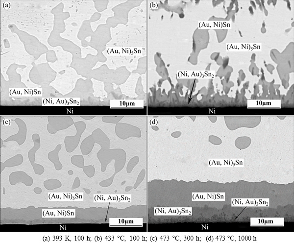
Fig. 4 Microstructures of AuSn20/Ni joints aging in various conditions
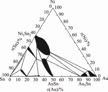
Fig. 5 Isothermal ternary phase diagram of Au-Ni-Sn at room temperature [17]
Furthermore, a new sprout-like intermetallic compound forms between the (Ni,Au)3Sn2 and Ni layer after 1000 h annealing at 473 K, as shown in Fig. 4(d). EPMA measurements show that the composition of the reaction product is 12.11%Au-51.15%Ni-36.74%Sn (mole fraction), which is inexistent in the Au-Ni-Sn ternary phase accurately. According to SONG��s [18] study, with <10% Ni in Au-Sn solder, the ternary system is equilibrium with ��+��(Ni)+Ni3Sn2(Au); with 20% Ni, the equilibrium system is composed of ��(Ni) and Ni3Sn2(Au); and with 35% Ni, the equilibrium system is (Au,Ni)Sn+Ni3Sn2(Au)+Ni3Sn(Au). This suggests that the new compound in our system may be (Ni,Au)3Sn phase.
3.3 Growth kinetics of IMC layer
The morphological change and the increased thickness of the IMC layer observed in the annealed specimens indicate the interfacial reaction of the solder with the Ni layer during the thermal annealing process. The increased thickness l of the IMC layer during annealing and the total thickness ls of the IMC layer can be denoted as
l=ls-l0 (1)
where l0 is the as-solidified thickness of IMC layer, which is about 0.4 ��m in this work.
The detecting results for l are plotted as triangles, open circles and squares for 393, 433, and 473 K in Fig. 6, respectively. Here, the ordinate indicates the logarithm of the thickness l, and the abscissa shows the logarithm of the aging time t. As it can be seen, the thickness l monotonically increases with increasing annealing time t at the three annealing temperatures. Furthermore, the plotted points for each thickness are located well on a straight line. Therefore, l is mathematically described as a function of t by
 (2)
(2)
where t0 is unit time, 1 s. It is adopted to make the ratio t/t0 dimensionless. The proportionality coefficient k has the same dimension as the thickness l, but the exponent n is dimensionless. The values of k and n in Eq. (2) are simultaneously determined from the plotted points in Fig. 6 by a least-squares method. Thickness l is calculated for 393, 433, 473 K annealing and shown as dashed, dotted and solid lines in Fig. 6, respectively. The higher the annealing temperature T is, the larger the thickness l is obtained at each annealing time. Thus, the overall growth rate of the intermetallic layer increases with the increasing annealing temperature.
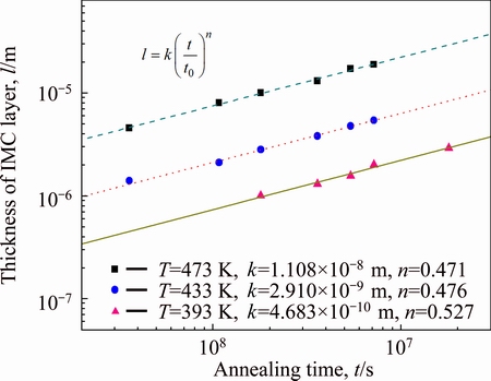
Fig. 6 Thickness l of IMC layer vs aging time t for AuSn20/Ni interface
The mean values of the exponent n for AuSn20/Ni couples are plotted against the annealing temperature T in Fig. 7. Here, the ordinate and the abscissa show n and T, respectively. The exponent n is equal to 0.471 at 473 K, and monotonically increases with decreasing annealing temperature. At 433 and 393 K, n is equal to 0.476 and 0.527, respectively. At the reactive diffusion interface, the mean values of the exponent n demonstrate the rate-controlling process of the diffusion couples. When the reactive diffusion is controlled by the volume diffusion of the constituent elements in each phase, n is equal to 0.5. However, the grain boundary diffusion across the intermetallic layer governs the reactive diffusion at low temperatures where the volume diffusion is practically frozen out. If the reactive diffusion is purely controlled by the grain boundary diffusion and grain growth occurs in the intermetallic layer according to the parabolic law, the exponent takes a value of n=0.25 [9]. According to the results in Fig. 7, the exponents n for all temperatures are close to 0.5. This indicates that the atomic diffusion of Ni and Sn through the interface IMC layer was the main controlling factor for the growth of the interface IMC during annealing. However, the value of n decreased slightly with increasing of annealing temperature. This suggests that the growth of IMC layer is unlikely to be controlled by just one mechanism. When the grain grows, the volume fraction of the grain boundary monotonically decreases with annealing time. Such decrease in the volume fraction causes the decrement of the effective cross section, and accelerates the grain boundary diffusion. As a result, the exponent n in Eq. (2) takes values a little bit less than 0.5.
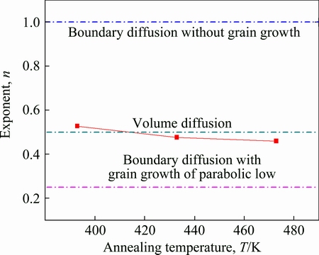
Fig. 7 Exponent n vs annealing temperature T
In the case of the reactive diffusion controlled by the volume diffusion, the growth of the intermetallic layer is expressed by the following equation [8]:
l2=Kt (3)
Equation (3) is another formula of the parabolic relationship, where K is the diffusion coefficient. As mentioned above, the volume diffusion is the rate-controlling process for AuSn20/Ni couple at 393-473 K. Thus, the values of K at 393, 433 and 473K were evaluated from Eq. (3) using the results in Fig. 5 by the least-squares method. The evaluation provides K=1.099��10-18, 1.671��10-17 and 1.134��10-16 m2/s for 393, 453 and 473 K, respectively. These values are plotted against the annealing temperature T as squares shown in Fig. 8. In this figure, the ordinate indicates the logarithm of K, and the abscissa shows the reciprocal of T. The temperature dependence of K is expressed by the following equation with certain accuracy [19]:
 (4)
(4)
where K0 and QK are the pre-exponential factor and the activation enthalpy, respectively. Determined from the plotted points in Fig. 8 by a least-squares method, we obtain K0=1.23��10-7 m2/s and QK =81.8 kJ/mol for the IMC layer in AuSn20/Ni diffusion couple.
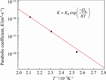
Fig. 8 Parabolic coefficient K vs reciprocal of annealing temperature T for AuSn20/Ni joints diffusion couple
4 Conclusions
1) Due to reflow soldering, the solder matrix is compound of (Au,Ni)Sn and (Au,Ni)5Sn, and the (Ni,Au)3Sn2 layer is formed at AuSn20/Ni interface.
2) After annealing at 393, 433 and 473 K, a compound IMC layer of (Au,Ni)Sn and (Au,Ni)3Sn2 is formed at AuSn20/Ni interface, and it grows remarkably with increasing annealing temperature and time. The thickness l of the IMC layer grows following the formula: l=k(t/t0)n. The values of exponent n vale for the composite IMC layer annealed at the three temperatures are 0.527, 0.476 and 0.471, respectively.
3) In the case of the reactive diffusion controlled by the volume diffusion for AuSn20/Ni diffusion couple, the pre-exponential factor K0=1.23��10-7 m2/s and the activation enthalpy QK=81.8 kJ/mol are obtained from the results of the parabolic coefficient K by a least-squares method.
References
[1] ZENG G, MCDONALD S, NOGITA K. Development of high- temperature solders: Review [J]. Microelectronics Reliability, 2012, 52: 1306-1322.
[2] WANG Y K, LIU W S, MAN Y Z, HUANG Y F, TANG Y, CHENG F, YU Q. Indentation size effect and micromechanics characterization of intermetallic compounds in the Au-Sn system [J]. Materials Science & Engineering A, 2014, 610: 161-170.
[3] LI Wei, XU Kun, CHEN Deng-quan, LUO Xi-ming, LIU Yi. Performance comparison between Au-Sn alloy solder paste and solder foil [J]. Precious Metals, 2013, 34(1): 25-28. (in Chinese)
[4] WEI Xiao-feng, WANG Ri-chu, PENG Chao-qun, FENG Yan. Interfacial reaction and shear strength of AuSn20/Ni solder joints [J]. The Chinese Journal of Nonferrous Metals, 2013, 23(7): 1907-1913. (in Chinese)
[5] CHUNG H M, CHEN C M, LIN C P, CHEN C J. Microstructural evolution of the Au-20wt.%Sn solder on the Cu substrate during reflow [J]. Journal of Alloys and Compounds, 2009, 485: 219-224.
[6] YOON J W, KIM S W, JUNG S B. Interfacial reaction and mechanical properties of eutectic Sn-0.7Cu/Ni BGA solder joints during isothermal long-term aging [J]. Journal of Alloys and Compounds, 2005, 391: 82-89.
[7] KIM S S, KIM J H, BOOH S W, KIM T G, LEE H M. Microstructural evolution of joint interface between eutectic 80Au-20Sn solder and UBM [J]. Materials Transactions, 2005, 46: 2400-2405.
[8] YATO Y, KAJIHARA M. Kinetics of reactive diffusion in the (Au-Ni)/Sn system at solid-state temperatures [J]. Materials Science and Engineering A, 2006, 428: 276-283.
[9] MITA M, MIURA K, TAKENAKA T, KAJIHARA M, KUROKAWA N, SAKAMOTO K. Effect of Ni on reactive diffusion between Au and Sn at solid-state temperatures [J]. Materials Science and Engineering B, 2006, 126: 37-43.
[10] VASSILEV G P, LILOVA K I, GACHON J C. Enthalpies of formation of Ni-Sn compounds [J]. Thermochimica Acta, 2006, 447: 106-108.
[11] DEBSKI A, GASIOR W, MOSER Z, MAJOR R. Enthalpy of formation of intermetallic phases from the Au-Sn system [J]. Journal of Alloys and Compounds, 2010, 491: 173-177.
[12] DEBSKI A, GASIOR W, MOSER Z, MAJOR R. Enthalpy of formation of Au-Sn intermetallic phases: Part II [J]. Journal of Alloys and Compounds, 2011, 509: 6131-6134.
[13] LAURILA T, VUORINEN V, KIVILAHTI J K. Interfacial reactions between lead-free solders and common base materials [J]. Materials Science and Engineering R, 2005, 49: 1-60.
[14] TUMMALA R R. Fundamentals of microsystems packaging [M]. HUANG Q G, TANG J Y. Translate. Nanjing: Southeast University Press, 2004: 175-189.
[15] LEE K Y, LI M, TU K N. Growth and ripening of (Au,Ni)Sn4 phase in Pb-free and Pb-containing solders on Ni/Au metallization [J]. Journal of Materials Research, 2003, 18: 2562-2570.
[16] TSAI J Y, CHANG C W, SHIEH Y C, HU Y C, KAO C R. Controlling the microstructure from the gold-tin reaction [J]. Journal of Electronic Materials, 2005, 34: 182-187.
[17] ANHOCK S, OPPERMANN H, KALLMAYER C, ASCHENBRENNER R, THOMAN L, REICHEL H. Investigations of Au/Sn alloys on different end-metallizations for high temperature applications [C]// Proceedings of the 22nd IEEE/CPMT International Electronics Manufacturing Technology Symposium, Berlin, Germany, IEEE, New York,1998: 156-165.
[18] SONG H G, AHN J P, MORRIS J W. The microstructure of eutectic Au-Sn solder bumps on Cu/electroless Ni/Au [J]. Journal of Electronic Materials, 2001, 30: 1803-1807.
[19] LEE T K, ZHANG S, WONG C C, TAN A C, HADIKUSUMA D. Interfacial microstructures and kinetics of Au/SnAgCu [J]. Thin Solid Films, 2006, 504: 441-445.
AuSn20/Ni�������֯����������仯�������������ѧ��Ϊ
ΤС��1����ѧ��1�����ճ�2
1. ����ũ�ֿƼ���ѧ ��е����ӹ���ѧԺ������712100��
2. ���ϴ�ѧ ���Ͽ�ѧ�빤��ѧԺ����ɳ410083
ժ Ҫ�����û����������Ʊ�AuSn20/Ni���㣬ͨ��ɨ��羵(SEM)�͵���̽��(EPMA)������������Ľ��淴Ӧ���˻��������֯���ݱ䣬��̽�ֽ�������仯����(IMC)����������ѧ�������������583 Kǥ����AuSn20/Ni�����γ�(Ni,Au)3Sn2 IMC�㣬����IMC����l�ı仯���˻�ʱ��t���ӳ����ϱ���ʽl=k(t/t0)n������ֱ���393��433��473 K���˻�ʱ����ϵָ��n�ֱ�Ϊ0.527��0.476��0.471�������ڵ���Һ�����¶��˻�ʱ��AuSn20/Ni����IMC��������������ɢ����Ϊ�������������ɢ��Ԥָ������K0�ͼ�����QK�ֱ�Ϊ1.23��10-7 m2/s��81.8 kJ/mol��
�ؼ��ʣ�AuSn20/Ni���㣻���淴Ӧ����������ѧ�������ɢ����
(Edited by Yun-bin HE)
Foundation item: Project (JPPT-125-GH-039) supported by the Ministry of Science and Technology of China; Project (Z109021567) supported by Fundamental Research Funds for the Central Universities, China
Corresponding author: Xue-wei ZHU; Tel: +86-15209261723; E-mail: zxw_83614@163.com
DOI: 10.1016/S1003-6326(17)60139-0
Abstract: The AuSn20/Ni joints were prepared by the reflow soldering technology and then annealed at solid-state temperature to form diffusion couples. The interfacial reactions and the growth kinetics of the intermetallic compounds (IMC) at the AuSn20/Ni soldering interface were investigated by scanning electron microscopy (SEM) and electron probe microanalysis (EPMA). The results show that, the (Ni,Au)3Sn2 phases are formed at the AuSn20/Ni interface after soldering at 583 K. The thickness l of the IMC layer monotonically increases with increasing annealing time t according to the relationship l=k(t/t0)n, where the exponent n is 0.527, 0.476 and 0.471 for 393, 433 and 473 K annealing, respectively. This indicates that the volume diffusion contributes to the growth of the IMC layer at the AuSn20/Ni interface at solid-sate temperature. The pre-exponential factor K0=1.23��10-7 m2/s and the activation enthalpy QK=81.8 kJ/mol are obtained from the results of the parabolic coefficient K by a least-squares method.
