

Influence of intermittently etching on quality of CVD diamond thin films
YANG Kan-cheng(��٩��)1, XIA Yi-ben(���屾) 1, WANG Lin-jun(���־�) 1, LIU Jian-min(������) 1, SU Qing-feng(�����) 1, XU Run(�� ��) 1, PENG Hong-yan(������) 2, SHI Wei-min(ʷΰ��) 1
1. School of Materials Science and Engineering, Shanghai University, Shanghai 200072, China;
2. Department of Physics, Mudanjiang Normal College, Mudanjiang 157012, China
Received 10 April 2006; accepted 25 April 2006
Abstract:
A new method, called growing-etching repetitional process based on hot filament chemical vapor deposition, was proposed to improve the quality of diamond film. During the deposition carbon source was intermittently closed letting hydrogen etch the surface of the diamond film from time to time. In order to find whether it is helpful to the films�� quality, a series of experiments were done. The results show that the new method can enhance the orientation of the chemical vapor deposition diamond films, reduce the graphite phase and increase the film��s surface resistivity.
Key words:
hot filament chemical vapor deposition; diamond film; intermittently etching;
1 Introduction
Diamond is prognosticated to substitute silicon and open a new age of particle detector attributing to its excellent physical-chemical properties[1]. However, the quality of the diamond thin film is the all-important factor of the detector performance[2] and is affected by lots of factors such as vapor pressure, carbon concentration, pre-treatment methods and substrate temperature[3-7]. However, each factor has its optimum value in a certain circumstance and with the environment condition changing, the value changes. Thus, it is hard to keep each parameter at optimum value during every experiment.
In this paper, we adopted a new kind of process by ignoring the environment factor. If the method works, it will improve the quality of chemical vapor deposition (CVD) diamond film through process instead of parameter. By far now, rarely groups have studied this process.
According to some references the existence of hydrogen can improve the quality of diamond thin film. And it is convinced that hydrogen etching can reduce the graphite content in diamond film. During the deposition process graphite phase is generated concomitantly, final etching can only remove the graphite phase on the surface of the film. Based on this viewpoint, carbon source was intermittently closed letting hydrogen etch the film from time to time to each the graphite phase inside the film. This paper is focused on studying wheatear the new process can really improve the quality of the diamond film when the growth environment is relatively stable.
2 Experimental
The experiment was based on hot filament chemical vapor deposition (HFCVD)[8]. The diamond thin films were deposited on Si (100) substrates with an area of 1cm��1cm. During each deposition process the growth parameters including carbon concentration, vapor pressure and growth temperature were kept at constant value (Table 1). And the total growing time was also kept at a fixed value (12 h). The only changing factors are the etching time and the frequency of closing the carbon source (Table 2).
In order to show whether the new process can really
Table 1 Necleation and growth parameters for diamond films by HFCVD
Table 2 Experiment parameters of four samples

improve the quality of the diamond film, each deposited film was characterized by XRD, AFM, I-V and Raman spectroscopy[9, 10].
3 Results and discussion
Fig.1 shows 3D images for four samples�� surfaces taken by AFM. With the frequency of closing the carbon source increasing, the film��s orientation is enhanced. Sample 3 shows (111) orientation while sample 4 shows (100) orientation obviously. Since hydrogen has the capability of selectively etching, the lower the planar density is, the more the hydrogen atom can cross the plane instead of impacting carbon atom. Thus, hydrogen��s etching effect on high planar density plane is more intensive.
Fig.2 shows XRD patterns of the four samples. According to the standard intensity of each peak in the PDF card, the ratios of the intensity of each peak were calculated. In response to the calculation, sample 3 shows (111) orientation, while sample 4 shows (100) orientation. Therefore, if hydrogen��s intermittently etching process is adopted, the orientation of the CVD diamond film is inclined to low planar density��s plane.
Raman spectroscopy was utilized to investigate the phase composition and the local stresses of the films. Fig.3 demonstrates the Raman spectra of the samples at different etch frequencies. The spectra are dominated by two distinct peaks. One is centered at 1 332 cm-1 associated with sp3 bonded carbon (i.e. diamond phase) and the other is centered at 1580cm-1 attributed to sp2 bonded carbon (i.e. graphite phase). The ratio of the intensity of the peak at 1 332 cm-1 to the peak around 1 550 cm-1 shows which one, diamond phase or graphite phase, is in the higher flight. The higher the ratio is, the more diamond phase the film has. The low ratio of sample 1 indicates that the film contains lots of graphite phase. Compared with sample 1, the other three samples�� graphite phase is obviously reduced. Therefore, frequent hydrogen etching does reduce the quantity of the graphite phase.
I-V curves were measured to attribute four samples�� electricity property (Fig.4). Intermittently hydrogen etching can efficiently reduce the quantity of graphite phase and increase the films�� surface electrical resistivity. With the etching time increasing, the resistivity augments. The resistivities of the four samples
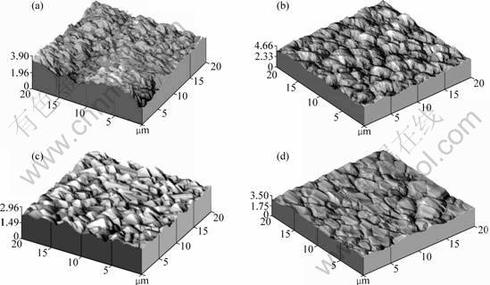
Fig.1 AFM images of samples at different etching frequencies: (a) Sample 1, 12 h-1; (b) Sample 2, 6 h-1; (c) Sample 3, 4 h-1;(d) Sample 4, 2 h-1

Fig.2 XRD patterns of samples at different etching frequencies: (a) Sample 1, 12 h-1; (b) Sample 2, 6 h-1; (c) Sample 3, 4 h-1; (d) Sample 4, 2 h-1
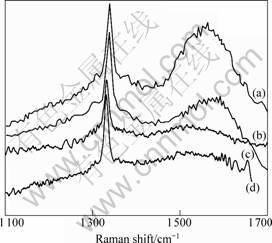
Fig.3 Raman spectra of samples at different etching frequencies: (a) Sample 1, 12 h-1; (b) Sample 2, 6 h-1; (c) Sample 3, 4 h-1; (d) Sample 4, 2 h-1

Fig.4 Dark current-voltage curves of samples at different etching frequencies
are 6.6��109, 1.19��1010, 1.6��1010 and 2��1010 W?cm, respectively. Compared with sample 1, the other three samples�� dark current is greatly reduced and the films�� surface electrical resistivity is increased. Though the hydrogen etching time in sample 4 is longer than that in sample 3, electrical resistivity of sample 4 is not improved obviously. It is because high frequent hydrogen etching restricts the growth of the grain. Compared with sample 3, sample 4 has more grain boundaries around which there are many great defects which will reduce the electrical resistivity.
4 Conclusions
During diamond films�� deposition intermittently hydrogen etching process is adopted to improve the quality of CVD diamond film. AFM, XRD, I-V and Raman spectroscopy��s analysis provide a clearly evidence that intermittently hydrogen etching can improve the quality of CVD diamond film. The process can efficiently increase the quantity of diamond phase in the film as well as the film��s surface electrical resistivity. In addition, this process can make the orientation of the film incline to the low planar density plane, which is more suitable for the application in thermology, photology and electronics.
References[1] MAINWOOD A. CVD diamond particle detectors[J]. Diamond and Related Materials, 1998, 7: 504-509.
[2] ZHOU H Y, ZHU X D, ZHAN R J. Application of CVD diamond film for radiation detection[J]. Nuclear Techniques, 2005, 28(2): 135-140.
[3] CHEN Z H, YU Z M, XU X Y, LIU W P. Effect of methane concentration on diamond film texture[J]. Diamond and Abrasives Engineering, 2005, 146(2): 21-24.
[4] MARINELLI M, MILANI E, MONYUORI M, PAOLETTI A, PAROLI P, THOMAS J. Effect of gas composition on texture of diamond films[J]. Appl Phys Lett, 1994, 65(22): 2839-2841.
[5] MARINELLI M, MILANI E, PAOLETTI A, SANTORO M, SCIORTINO S, TUCCIARONE A, VERONA-RINATI G. Methane-induced texturing of chemical vapor deposition diamond films and correlation with UV photoreponse[J]. Diamond and Related Materials, 1998, 7: 1039-1042.
[6] ZHANG X X, SHI T S, WANG J X, ZHANG X K. Oriented growth of a diamond film on Si(100) by hot filament chemical vapor deposition[J]. Journal of Crystal Growth, 1995, 155: 66-69.
[7] HUANG J T, YEH W Y, HWANG J, CHANG H. Bias enhanced nucleation and bias textured growth of diamond on silicon(100) in hot filament chemical vapor deposition[J]. Thin Solid Films, 1998, 315: 35-39.
[8] ZHANG Z M, XIN H W, DAI Y B, SUN F H, WANG T, SHEN H S. Synthesis of nanocrystalline diamond films deposited by hot filament CVD[J]. Microfabrication Technology, 2003, 1: 27-33
[9] SPEAR K E. Diamond-ceramic coating of the future[J]. Journal of American Ceramics Society, 1989, 72: 171-191.
[10] WEIMA J A, JOB R, FAHMER W R, KOSACA G C, MILLER N, FRIES T. Surface analysis of ultraprecise polished chemical vapor deposited diamond films using spectroscopic and microscopic techniques[J]. J Appl Phys, 2001, 89: 2434-2440.
Foundation item: Project (60577040) supported by the National Natural Science Foundation of China; Project (0404) supported by the Shanghai Foundation of Applied Materials Research and Development; Projects (0452nm051, 05nm05046) supported by the Nano-Technology Project of Shanghai; Project (T0101) supported by the Shanghai Leading Academic Disciplines
Corresponding author: WANG Lin-jun; Tel: +86-21-56333514; Fax: +86-21-56332694; E-mail: ljwang@staff.shu.edu.cn
