Trans. Nonferrous Met. Soc. China 25(2015) 3279-3285
Identification and characterization of single crystal Bi2Te3-xSex alloy
Emina  1, Svetlana IVANOV2, Zoran
  2, Ljiljana
  3, Rudolf TOMANEC3, Lidija
  1, Ana KOSTOV1
1. Mining and Metallurgy Institute Bor, Zeleni bulevar 35, Bor 19210, Serbia;
2. Technical Faculty Bor, University of Belgrade, VJ 12, Bor 19210, Serbia;
3. Faculty of Mining and Geology, University of Belgrade,  7, Belgrade 11000, Serbia
Received 6 November 2014; accepted 6 April 2015
Abstract: The results of experimental investigation of n-type semiconductor based on Bi2Te3 alloy were presented. This material is used in manufacture of thermoelectric coolers and electrical power generation devices. Bi2Te2.88Se0.12 solid solution single crystal has been grown using the Czochralski method. Monitoring of structure changes of the sample was carried out by electron microscope. The elemental composition of the studied alloy was obtained by energy dispersive spectrometry (EDS) analysis and empirical formula of the compound was established. X-ray diffraction analysis confirmed that the Bi2Te2.88Se0.12 sample was a single phase with rhombohedral structure. The behavior upon heating was studied using differential thermal analysis (DTA) technique. Changes in physical and chemical properties of materials were measured as a function of increasing temperature by thermogravimetric analysis (TGA). The lattice parameters values obtained by X-ray powder diffraction analyses of Bi2Te2.88Se0.12 are very similar to Bi2Te3 lattice constants, indicating that a small portion of tellurium is replaced with selenium. The obtained values for specific electrical and thermal conductivities are in correlation with available literature data. The Vickers microhardness values are in range between HV 187 and HV 39.02 and decrease with load increasing. It is shown that very complex process of infrared thermography can be applied for characterization of thermoelectric elements and modules.
Key words: Bi2Te3; Bi2Te3-xSex; single crystal; semiconductor; thermoelectrical properties; hardness; thermovision imaging
1 Introduction
Semiconductors are materials whose electronic properties depend on the energy gap (Eg) width or band gap and dopant concentration. It is well known that semiconductors with a relatively small band gap exhibit very good thermoelectric performance [1-3]. The Eg of semiconductors is relatively small [4] and at the room temperature (300 K) it is 0.66 eV. The energy gap of Bi2Te3 single phase varies with temperature and it is 0.13 [5], 0.15 [6,7], 0.21 eV [8] at room temperature.
Tellurium (Te) and selenium (Se) belong to twelve elementary semiconductors. Elementary semiconductors are those in which the properties are dependent on the semiconductor electronic structure. The presence of impurities even in very small proportions can have large effects on the properties of the thermoelectric material [9]. Therefore, the conductivity of semiconductors may easily be modified by introducing dopants into their crystal structure.
The n-type Bi2Te3-xSex semiconductors are well known to have excellent thermoelectric properties near room temperature, and are used in thermoelectric cooling devices and electrical power generation devices. Many studies on these materials have been performed in order to increase the figure of merit, Z, the parameter which evaluates the quality of thermoelectric material [10]. The figure of merit for the undoped Bi2Te3 at room temperature is 0.6 [11]. Thermal conductivity can provide information about the temperature range of operation [12]. Typical values of elemental semiconductors for the Seebeck coefficient (S), electrical conductivity (��), thermal conductivity (��) and figure of merit (ZT) at room temperature are: S=200��10-6 V��K-1, ��=105 ��-1��m-1, ��=1-100 W��m-1��K-1, ZT=0.1-1.0, where T is the temperature [13].
The electric conductivity is a characteristic of each material [14]. Only semiconductors offer the right combination of high Seebeck coefficient, high electrical conductivity and low thermal conductivity.
The change in ZT with temperature for most of the known thermoelectric n-type materials studied to date is shown in Fig. 1.
The values of Bi2Te3-xSex alloy for electrical resistivity (��), the Seebeck coefficient (S), power factor (FP) and thermal conductivity (��) at 250-350 K are: ��=10��10-6 ����m, S=-200��10-6 V��K-1, FP=40��10-4 W��m-1��K-2, ��=1.4 W��m-1��K-1 [13].
The negative value of the Seebeck coefficient means that the major charge carriers in the sample are electrons.
Bi2Te3 has the tetradymite-type rhombohedral structure [14-18]. Bi2Te3 melting point is 585 ��C [18,19].
The objective of this work is to supplement knowledge of the structure, mechanical and thermoelectrical properties of Bi2Te3-xSex alloy.

Fig. 1 Value of ZT for most of known thermoelectric n-type semiconductors [10]
2 Experimental
Bi2Te2.88Se0.12 sample was synthesized using the Czochralski method. Single crystals of 20 mm in length and 8 mm in diameter were obtained by this method. The obtained sample of semiconductor was examined using SEM-EDS, XRD, four probe method for measuring electrical conductivity, Hartman method for measuring specific heat conductivity, DTA, TGA and microhardness measurements. Thermovision imaging was carried out. Structural analysis was done [20] using a Reichert MeF2 microscope (magnification up to 200) and SEM-EDS. Surfaces of the polished sample for light optical microscopy (LOM) and SEM-EDS prior to metallographic analysis, were etched with hydrofluoric, nitric and acetic acid etching solution to reveal the structure of the investigated sample [21]. EDS analysis was done to determine chemical composition of the studied sample as well as to check sample homogeneity.
The sample was further powdered for XRD analyses. X-ray intensity measurement was carried out on a PHILIPS PW 1710 automated diffractometer using monochromatized Cu Ka radiation (l=1.54178  ) and step-scan mode (2q range was from 4�� to 90��, step 0.02��, time 0.5 s). The specific electrical conductivity of the sample d8 mm �� 20 mm was measured at 25 ��C. Four probe method was used.
The specific thermal conductivity was measured on the same sample and at the same temperature. Harman method was applied.
Phase transition temperatures and the physical property of the sample were analyzed using TG�CDTA technique. Differential thermal analysis (DTA) and TG measurements were carried out using SDT Q60 (firm TA instruments) apparatus.
Microhardness was measured using instrument PTM-3 with Vicker��s diamond pyramid (Vickers indenter). All the measurements were made at room temperature, and the indentation time was kept at 15 s. Microhardness values vary with load and work- hardening effects of materials. The applied indenter load was varied from 15 to 150 g, and the diagonal of the impression was measured. Hardness of the crystals was calculated using the relation:
HDP=1.8544 P/d2 (1)
where HDP is the Vickers microhardness value; P is the indenter load in kg; and d is the diagonal length of the impression in mm. On each surface, several trials of indentation are taken and the average value of hardness is found.
In these researches, the digital thermal imaging camera Wohler IK 21, whose operation is based on a uncooled germanium thermoelectrical linear detector, has been used.
Thermovision imaging is a non-contact method within real-time register emission of heat or infrared radiation. Since all the bodies emit heat in this way, we can get a clear idea about the temperature of a body in relation to the environment in which the body is. There is almost no area in which this powerful technique is not applied. It is simple to use environmentally and friendly [22,23].
3 Results and discussion
3.1 SEM-EDS analysis
Chemical analysis was done using SEM-EDS giving empirical formula of the compound as Bi2Te2.88Se0.12. SEM image with marked points of EDS chemical analysis of the investigated sample is presented in Fig. 2, while the results of experimental determination of composition by EDS are presented in Table 1.
Figure 2 shows the cracks which appear in the crystal. Special growth conditions are necessary for avoiding these cracks. A low temperature gradient in the melt and solid is necessary for achieving low dislocation density or strain in the crystal. The role of melt stirring during crystal growth is also crucial.

Fig. 2 SEM image (with investigated points) of longitudinal section of Bi2Te2.88Se0.12 sample
Table 1 Results of SEM-EDS analysis of investigated sample Bi2Te2.88Se0.12

Concentrations of elements in studied points are function of the peak areas in EDS diagram (Fig. 3).
The obtained chemical compositions in the investigated points are similar, which means that the sample has uniform chemical composition (Table 1).
3.2 XRD analysis
Lattice constants of powdered Bi2Te2.88Se0.12 were determined by XRD analysis. The powder XRD patterns of Bi2Te2.88Se0.12 given in Table 2 and Fig. 4, show the presence of only one crystalline phase of a relatively high degree of crystallinity. All reflections in the XRD pattern of Bi2Te2.88Se0.12 were indexed to be a hexagonal unit cell: a=4.368(2), c=30.418(11)  , V= 502.5(4)
  3, which is very similar to a=4.3896(2), c= 30.5019(10)
  , V=508.99(4)
  3 for Bi2Te3 [24] and shows that a small portion of Te is replaced with Se. The incorporation of smaller Se leads to the lattice contraction and therefore all diffraction lines were slightly shifted toward bigger 2q angles with respect to Bi2Te3 lines (Fig. 4). Diffraction peaks of basal reflections (specially (0 0 3), (0 0 6) and (0 0 15)) are much more intense than the calculated ones, indicating the existence of preferred orientation due to the layered structure and perfect basal cleavage (Fig. 4).

Fig. 3 EDS spectrum 1 (a) and spectrum 2 (b) of Bi2Te2.88Se0.12
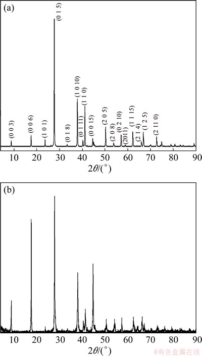
Fig. 4 Calculated XRD pattern of Bi2Te3 (a) using structural data given in Ref. [24] and measured powder XRD pattern of Bi2Te2.88Se0.12 (b)
Table 2 XRD powder diffraction data for Bi2Te2.88Se0.12

All semiconductors of the general formula Bi2Te3-xSex are solid solutions, which are isostructural with the Bi2Te3. They crystallize in the rhombohedral space group  (No. 166), and have layered structure of Bi2Te3 type. Chalcogens Ha in the structure are placed in two different Wyckoff positions: 3a and 6c, while the Bi atoms are found in 6c. Each chalcogen in the 3a position, Ha(3a), has 6 neighbouring Bi atoms, while chalcogen in the 6a position, Ha(6c), has 3 neighbours. This difference in coordination causes different lengths of Ha��Bi bonds: Ha(3a)��Bi bonds are longer and Ha(6c))��Bi bonds are shorter.
The basic part of the structure consists of five layers ��[Ha(3a)]��Bi(6c)��[Ha(6c)]��Bi(6c)��[Ha(3a)]��. Layers of the Bi and chalcogens are distributed alternately along the hexagonal c axis and they are linked by the weak van der Waals bonds.
3.3 Thermoelectric properties
Electrical conductivity ��, Seebeck coefficient S and thermal conductivity �� have been measured to define quality. These properties strongly depend on carrier concentration, mobility, crystal structure and defects in the crystal structure. Values of Bi2Te2.88Se0.12 crystal for electrical conductivity (��), the Seebeck coefficient (S) and thermal conductivity (��) at 298 K are: ��=1.03��105 S��m-1, S=207��10-6 V��K-1, ��=1.77 W��m-1��K-1.
ZHANG at al [25] have investigated 1-D/3-D structured AgNWs/Bi2Te3 nanocomposites and found that thermoelectric properties have been dramatically enhanced. Different researches have studied improvement of thermoelectric performance of nanocomposites, too [26-28].
3.4 Differential thermal analysis (DTA)
DTA was carried out under following conditions: air atmosphere, heating rate 10 ��C/min, and Tmax=800 ��C. Al2O3 was used as a referent material during the measurements. The precision of the measurement in the investigated temperature interval was 2.5 ��C. The total mass of the material was 1 g.
Obtained liquidus temperature (613.7 ��C) in Fig. 5 is close to melting temperature of Bi2Te3 compound, but slightly increased, which can be contributed to the presence of Se. The obtained DTA results imply that the tested material is stable to about 400 ��C. The first endothermic reaction at 409.7 ��C corresponds to the formation of �� phase (Bi2Te2Se) which is affirmed in the studies reported by SOKOLOV et al [29] and LAHALLE et al [30]. The second reaction obtained at temperature of 491.3 ��C does not correspond to any phase transformation which may be related to the binary phase diagram of Bi-Te or with phase transformations on Bi-Se binary diagram. We assumed that the second obtained temperature on the DTA curve refers to reaction of two phases: a Bi2Te3-based solid solution (��1) and a Bi2Te2Se (��) [26]. In this work, the range of Bi2Te3-xSex solid solution was determined.
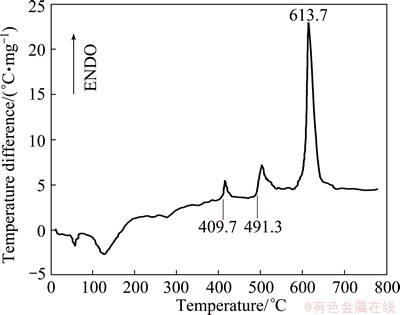
Fig. 5 DTA curve of Bi2Te2.88Se0.12 crystal
TGA was carried out under following conditions: heating rate, 10 ��C/min, sample mass 0.182 g, Tmax= 500 ��C in air medium. The curves obtained from thermogravimetric analysis and thermogravimetric (TG) curve show the sample change in mass depending on temperature (Fig. 6). The compound is stable up to 350 ��C and, after that, its mass increases which may be due to the undergoing reaction of an intermediate product with nitrogen. This is affirmed in the study reported by DHEEPA et al [31]. HANEMAN [32] has noted that the absorption of gases (O2, N2, CO2) on the obtained bismuth telluride samples is small.
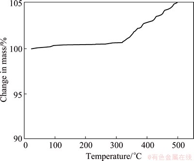
Fig. 6 TG curve of Bi2Te2.88Se0.12 crystal
3.5 Microindentation hardness studies
Structural defects in tested material must affect the results of microhardness measurements. Hardness measurements quantify the resistance of a material to plastic deformation. Microhardness and dislocation density in the case of semiconducting crystals are interrelated.
Table 3 Microhardness of n-type investigated Bi2Te2.88Se0.12 crystal
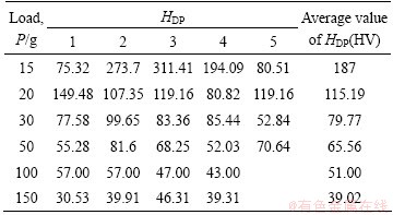
Figure 7 shows the variation of hardness with load for bismuth telluride, doped with Se. Hardness decreases with load.
According to literature, undoped single crystals of Bi2Te3 have Knoop of 155 N/mm2 [33]. Since the paper presents different methods of measuring microhardness, the comparative analysis of the obtained results and available literature data is not possible.
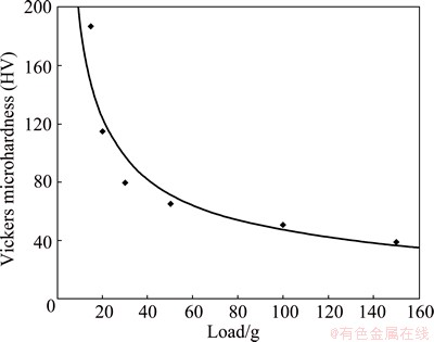
Fig. 7 Variation of microhardness with load for single crystal Bi2Te2.88Se0.12 at room temperature
3.6 Thermovision imaging of TE module
In order to test the efficiency of thermoelectric elements based on Bi2Te3 module, 27 elements of the p type measuring of 3 mm �� 3 mm �� 5 mm and 27 elements of the n type of the same size were developed (Fig. 8). Thermoelectric material of the p-type for the TE modules is Bi0.5Sb1.50Te2.98Se0.02 doped with zirconium.

Fig. 8 Thermoelectric module
Thermovision imaging of the module is shown in Fig. 9. One side of the module is heated up to 80 ��C and then allowed to naturally cool down. The other side is passively cooled to about 22 ��C. The module is loaded by thermogenic consumer of 2.2 �� resistivity in order to obtain the maximum usable power since in the observing temperature range the internal resistance of the module is approximately constant with amount of 2.2 �� resistivity. The resulting dependence of the output (electricity) power from the temperature difference at the hot and cold sides is shown in Fig. 10.
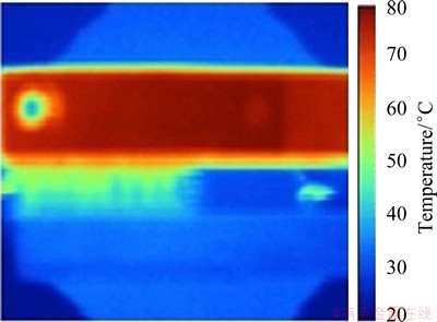
Fig. 9 Thermovision record of thermoelectric module
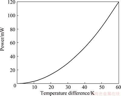
Fig. 10 Dependence of 30 W thermoelectric module output power from temperature difference of hot and cold sides
Figure 10 shows that the temperature difference between the hot and the cold sides is crucial for obtaining significant power at the output of the thermoelectric module.
4 Conclusions
1) A single crystal Bi2Te2.88Se0.12 was investigated using different experimental methods, such as light optical microscopy, SEM-EDS, microhardness analysis, XRD, Four Probe Method, Harman method, TG-DTA and thermovision.
2) EDS analysis was done to determine chemical composition of the studied alloy. The results of the analysis are presented in this work together with the mole ratios of Bi to Te to Se.
3) By methods of differential thermal analysis and X-ray phase analysis, it is proved that the Bi2Te3-Bi2Se3 section is a system with a continuous series of solid solutions, with the formation of Bi2Te2.88Se0.12 compound below the solidus line. DTA of the material shows the endothermic heat transfer during the process.
4) Microhardness of investigated Bi2Te2.88Se0.12 single crystal alloy in the range of HV 39 to HV 187 is examined using different loads and obtained dependence is presented graphically. In order to test the efficiency of thermoelectric elements based on Bi2Te3 module, thermovision imaging is done. It is shown that thermal imaging research can be a simple tool for analyzing the heating uniformity of thermoelectric module.
Acknowledgement
The authors are grateful to the Ministry of Education, Science and Technological Development of the Republic of Serbia for financial support of projects: ��Development of ecological knowledge-based advanced materials and technologies for multifunctional application�� (Grant No. TR34005) and ��New approach to designing materials for energy conversion and storage�� (Grant No. OI172060) and ��0-3D nanostructures for application in electronics and renewable energy sources: synthesis, characterisation and processing�� (Grant No. III45007).
References
[1]  E, IVANOV S,
  Z,
Z,  N,
N,  L,
L,  I. SEM-EDS analysis and microindention hardness study of n-type doped BiTeSe alloy single crystals [C]//Proceedings of the 45th International October Conference on Mining and Metallurgy. Bor, Serbia: IRM, 2013: 584-587.
[2] WANG Yi-fu, XIA Qing-lin, PAN Liu-xian, YU Yan. First principles calculation on ternary stannide phase narrow band gap semiconductor Na2MgSn [J]. Transactions of Nonferrous Metals Society of China, 2014, 24(6): 1853-1858.
[3]  N. Thermal diffusivity of single crystal Bi0.9Sb0.1 [J]. Science of Sintering, 2010, 42: 45-50.
[4]  V. Semiconductor diodes and transistors [M]. 3rd ed. Beograd: Newspaper-Publishing Company, 1975. (in Serbian)
[5] KAVEI G, KARAMI M A. Thermoelectric crystals Bi2Te2.88Se0.12 undoped and doped by CdCl2 or CdBr2 impurities, fabricated and characterized by XRD and Hall effect [J]. Materials Research Bulletin, 2008, 43: 239-243.
[6] TRIPATHI M N, BHANDARI C M. Material parameters for thermoelectric performance [J]. Journal of Physics, 2005, 65(3): 469-479.
[7] HOCHBAUM A I, CHEN R, DELGADO R D, LIANG W, GARNETT E C, NAIARIAN M, MAJUMDAR A, YANG P. Enhanced thermoelectric performance of rough silicon and nanowires [J]. Nature, 2008, 451 (7175): 163-167.
[8]  S. Electronic components [M].
  : Faculty of Electronic Engineering of
  , 2011. (in Serbian)
[9] GROVENOR C. Microelectronic materials [M]. Great Britain: Taylor & Francis Group, 1989.
[10] SUMIGA I, GRDJAN M, HUDJEK J. Thermoelectric modules- physical fundamentals and guidelines for use [J]. Technical Bulletin, 2007, 1(1-2): 5-10. (in Serbian)
[11]  P J. Thermoelectric effect and reuse of heat losses [C]//Renewable Energy Sources and Sustainable Development. Banja Luka: BIH, 2011: 207-214.
[12] BEJENARI M, KANTSER V. Thermoelectric properties of n-type Bi2Te3 wires [J]. Moldavian Journal of the Physical Sciences, 2004, 3(1): 94-99.
[13] FLEURIAL P J. Design and discovery of highly efficient thermoelectric materials [2015-03-31]. http://materialsforenergy. typepad.com/files/design-and-discovey-2.p df
[14] MISHRAYZ S K, SATPATHVYZ S, JEPSENZ O. Electronic structure and thermoelectric properties of bismuth telluride and bismuth selenide [J]. Journal of Physics-Condensed Matter, 1997, 9: 461-470.
[15] HONG Soon-jik, CHUN Byong-sun. Microstructure and thermoelectric properties of n-type 95%Bi2Te3-5%Bi2Se3 alloy produced by rapid solidification and hot extrusion [J]. Materials Research Bulletin, 2003, 38: 599-608.
[16] WIESE J R, MULDAWER L. Latice constants of Bi2Te3�CBi2Se3 solid solution alloys [J]. Journal of Physics and Chemistry of Solids, 1960, 15(1-2): 13-16.
[17] BOUANANI GHOUMARI H, EDDIKE D, LIAUTARD B, BRUN G. Solid state demixing in Bi2Se3�CBi2Te3 and Bi2Se3�CIn2Se3 phase diagrams [J]. Materials Research Bulletin, 1996, 31(2): 177-187.
[18] GOL��CMAN B M, KUDINOV V A, SMIRNOV I A. Semiconductor thermoelectric materials based on Bi2Te3 [M]. 2nd ed. Moskva: Nauka, 1972. (in Russian)
[19] SATTERTWAITE B, URE R. Electrical and thermal properties of Bi2Te3 [J]. Physical Review, 1957, 108(5): 1164-1169.
[20]  E, IVANOV S,
  Z,
Z,  B. Investigation of Bi-Sb-Te-Se-Sn-Zr alloy structure, part I [C]//Proceedings of the 44th International October Conference of Mining and Metallurgy. Bor, Serbia: IRM, 2012: 433-436.
[21] COLIN S, BRANDES E. Metals reference book [M]. 5th ed. London and Boston: Butter Workths, 1976.
[22]  Z,
Z,  D. Thermal vision application [M]. Bor: University of Belgrade, Technical Faculty Bor. (in Serbian)
[23]  E,
E,  Z, IVANOV S,
  L,
L,  V. Investigation of Bi-Sb-Te-Se-Sn-Zr alloy structure, part II [C]//Proceedings of the 44th International October Conference of Mining and Metallurgy. Bor, Serbia: IRM, 2012: 511-516.
[24] ATUCHIN V V, GAVRILOVA T A, KOKH K A, KURATIEVA N V, PERVUKHINA N V, SUROVTSEV N V. Structural and vibrational properties of PVT grown Bi2Te3 microcrystals [J]. Solid State Communications, 2012, 152: 1119-1122.
[25] ZHANG Qi-hao, AI Hin, WANG Wei-jie, WANG Lian-jun, JIANG Wan. Preparation of 1-D/3-D structured AgNWs/Bi2Te3 nanocomposites with enhanced thermoelectric properties [J]. Acta Materialia, 2014, 73: 37-47.
[26] ZHANG Qi-hao, AI Xin, WANG Lian-jun, CHANG Yan-xia, LUO Wei, JIANG Wan, CHEN Li-dong. Improved thermoelectic performance of silver nanoparticles-dispersed Bi2Te3 composites deriving from hierarchical two-phased heterostructure [J]. Advanced Functional materials, 2015, 25: 966-976.
[27] KIM M Y, YU B K, OH T S. Thermoelectric characteristics of the p-type (Bi0.2Sb0.8)2Te3 nanocomposites processed with SbTe nanowire dispersion [J]. Electronic Materials Letters, 2012, 8: 269-273.
[28] YEE K S, COATES E N, MAJUMDAR A, URBAN J J, SEGALMAN A R. Thermoelectric power factor optimization in PEDOT:PSS tellurium nanowire hybrid composites [J]. Physical Chemistry Chemistry Physics, 2013, 15: 4024-4032.
[29] SOKOLOV O B, SKIPIDAROV S Y A, DUVANKOV N I, SHABUNINA G G. Phase relations and thermoelectric properties of alloys in the Bi2Te3-Bi2Se3 system [J]. Inorganic Materials, 2007, 43: 8-11.
[30] LAHALLE G C, SCHERRER H, SCHERRER S. Growth of n-type Bi2Te2.55Se0.45 single crystal solid solution by the travelling heater method [J]. Journal of Physics and Chemistry of Solids, 1996, 57: 1713-1717.
[31] DHEEPA J, SATHYAMOORTHY R, VELUMANI S, SUBBARAYAN A, NATARAJAN K, SEBASTIAN P J. Electrical resistivity of thermally evaporated bismuth telluride thin films [J]. Solar Energy & Materials Solar Cells, 2004, 81: 305-312.
[32] HANEMAN D. Adsorption and bonding properties of cleavage surfaces of bismuth telluride [J]. Physical Review, 1960, 119: 567-574.
[33] BERGER L. Semiconductor materials [M]. NW, USA: CRC Press, 1997.
����Bi2Te3-xSex�Ͻ�ļ��������
Emina  1, Svetlana IVANOV2, Zoran
  2, Ljiljana
  3, Rudolf TOMANEC3, Lidija
  1
1
1. Mining and Metallurgy Institute Bor, Zeleni bulevar 35, Bor 19210, Serbia;
2. Technical Faculty Bor, University of Belgrade, VJ 12, Bor 19210, Serbia;
3. Faculty of Mining and Geology, University of Belgrade,  7, 11000 Belgrade, Serbia
ժ Ҫ���о�����Bi2Te3�Ͻ��n�Ͱ뵼���ʵ���Ʊ����ò��Ͽ������Ʊ��ȵ�ɢ�����ͷ����豸������Czochralski���Ʊ�Bi2Te2.88Se0.12���ܵ����塣���õ��������о���Ʒ����֯�仯������EDS����ʵ��Ͻ�ijɷ֣���ȷ��������ľ������ʽ��XRD����Bi2Te2.88Se0.12��ƷΪ����б��������ṹ�ĵ��������ò��ȷ����о��Ͻ�ļ�����Ϊ���������ط����о����ϵ������ͻ�ѧ�������¶ȵı仯����XRD�����õ���Bi2Te2.88Se0.12���������Bi2Te3�ķdz����������ֻ���ٲ���Te��Seȡ�������õĵ����ıȵ絼�ʺͱ��ȵ����������������������ά����Ӳ��ΪHV 187~39.02���������غ����ӣ�Ӳ�Ƚ��͡�����������Բ��ú����ȳ����ȵ�Ԫ����ģ����б�����
�ؼ��ʣ�Bi2Te3��Bi2Te3-xSex���������뵼�壻�ȵ����ܣ�Ӳ�ȣ����ӳ���
(Edited by Yun-bin HE)
Corresponding author: Emina  ; Tel: +381-30-454258; Fax: +381-30-435175; E-mail: emina.pozega@irm.bor.co.rs
DOI: 10.1016/S1003-6326(15)63964-4