Trans. Nonferrous Met. Soc. China 23(2013) 2939-2944
Microstructures and mechanical properties of electroplated Cu-Bi coatings
Xiao-jin WEI1, Wei-wei CHEN1, Yu-xin WANG1, See-Leng TAY1,2, Wei GAO1
1. Department of Chemicals and Materials Engineering, The University of Auckland, PB 92019, Auckland 1142, New Zealand;
2. Department of Mechanical Engineering, University of Malaya, Kuala Lumpur 50603, Malaysia
Received 5 November 2012; accepted 12 June 2013
Abstract: Electroplating has been used to produce Cu-Bi coatings. The crystal structure and lattice parameters of Cu in Cu-Bi composite coating were measured and compared with Cu coating. The mechanical properties of the coatings were also studied. It was found that the deposition parameters have significant effect on the mechanical properties of the Cu-Bi coatings. The microhardness has been improved from HV50165 of Cu coating to HV50 250 of Cu-Bi composite coating prepared at 50 mA/cm2 for 20 min. Correspondingly, wear resistance of the Cu-Bi composite coating has also been enhanced significantly.
Key words: Cu-Bi coating; composite coating; microhardness; coefficient of friction; electroplating
1 Introduction
Cu and Cu alloys are widely used in electrical industry due to their good conductivity [1]. Cu-based coatings and thin films have also been used for conducting purpose. One of the important industrial applications of Cu and Cu coatings is for electric contacts, which require both high conductivity and good wear resistance. However, the mechanical properties of Cu coatings including hardness and wear resistance are not good enough [1,2]. A variety of methods were developed to improve the mechanical properties of Cu alloy or Cu alloy coatings.
For instance, Ni coating on Cu showed that the average hardness of Ni coating was five times that of pure Cu [3]. Ni�CCu coating on Cu substrate obtained by pulsed laser deposition possessed significantly improved wear properties [4]. Cu-Cr-S coating by electro- depositing in acidic copper sulphate electrolytes containing a metallic powder of Cr displayed higher wear resistance compared with pure Cu coating [5]. The sol-gel based protective hybrid coatings were used to improve the hydrophobic properties and wear and corrosion resistance [6]. A combination of PVD and electroless Ni-P coatings was deposited on Cu alloy substrates to improve the wear resistance [7]. The nanocrystalline Cu-Ni films made by electrodeposition showed improved mechanical properties [8]. Report also indicated that the wear resistance of Cu-CeO2 nanocomposite coatings synthesized by pulse electro- deposition is superior to that of pure Cu [9].
The above quoted solid solution is a traditional way to improve the mechanical properties of Cu and Cu coatings. However, this method relies on lattice distortion that decreases the electric conductivity significantly. It has been known that Cu and Bi do not dissolve with each other so do not form a solid solution [10,11]. Addition of Bi should form a mixture of two separate phases. It was hoped that the two-phase structure can provide good dispersion strengthening effect without causing the misfit of Cu lattice [12-14], therefore can keep its good electrical conductivity.
Electroplating method was used to make the coatings because it is a common industrial process and can produce a finely mixed microstructure. This research aims at the development of electroplated Cu-Bi coatings with improved mechanical properties and good electric conductivity. This paper reports the deposition processing, coating microstructure and mechanical property of the Cu-Bi coating.
2 Experimental
Pure Cu sheets (purity>99.9%) were used as the substrate with dimensions of 10 mm��10 mm��3 mm. The specimens were mechanically polished using SiC papers to a grit of 1200#, then degreased ultrasonically in acetone. The pre-treatment for Cu substrate includes washing in solution containing 20 g/L citric acid and 60 g/L ammonium citrate, followed by anodizing at 2.5 mA/cm2 for 20 s. A two-electrode system was set up for the deposition of Cu on Cu substrate in the electrolyte containing 110 g/L K4P2O7, 40 g/L CuSO4��5H2O and 10 g/L Na2HPO4.
The solution for Bi electroplating contained 0.2 mol/L Bi(NO3)3��5H2O, 0.2 mol/L tartaric acid and 2.5 mol/L KOH, using NaOH solution to adjust pH value to 12. The electrolyte for Cu-Bi coating deposition was made by adding 1 mL of Bi electroplating solution into 70 mL Cu electrolyte. It was found that the electroplating current density has a significant effect on the coating composition and properties. The present work used 3 current densities, 10, 50 and 100 mA/cm2, to deposit Cu and Cu-Bi coatings. In order to obtain coatings with similar thickness for comparison, we used coating time of 30, 20 and 10 min for the deposition with current densities of 10, 50 and 100 mA/cm2, respectively.
The morphology and Bi concentrations in the Cu-Bi coatings were measured by a field emission scanning electron microscope (FESEM) with EDS attachment. The phase structure of the coatings was determined using X-ray diffraction (XRD). The coating hardness was measured using a microhardness tester (Leco M400) with a Vickers diamond indenter. The applied load was 50 g with a holding time of 15 s. At least 5 measurements under the same conditions were conducted, and the average value was used as the microhardness (HV). The standard deviation was also calculated. The wear property of coatings was tested using a micro-tribometer, with a friction counterpart of a ruby ball of 6 mm in diameter. A load of 1 N and a sliding speed of 50 mm/s were used at room temperature with the relative humidity of ~50%; the total elapsed time was 60-100 min. The electrical resistivity of the samples was measured by four-point probe method, then converted to the international standard unit (����m).
3 Results and discussion
3.1 Cross-sectional morphologies of coating
Figure 1 shows the cross-sectional morphologies of Cu and Cu-Bi composite coatings. In this research, different current density and deposition time were used in order to achieve a similar deposition thickness. Cu and Cu-Bi coatings which were deposited at 50 mA/cm2 for 20 min had a similar thickness of ~13 ��m (Fig. 1(a2) and (b2)). Both had the compact morphology. However, at the higher current density, the Cu-Bi had a porous microstructure (Fig. 1(b3)).
Figure 2 shows the EDS analysis of Cu and Cu-Bi coatings prepared at 50 mA/cm2 for 20 min. Bi was detected and its content is shown in Fig. 3. The content of Bi peaked at ~3.1% at the current density of 50 mA/cm2. A lower content of ~2.1% Bi was obtained at a higher current density of 100 mA/cm2. This might be due to the shorter time for Bi to deposit on substrate at the higher current density. The content of Bi depends on both current density and deposition time. Further studies are needed to investigate this effect.
3.2 Phase structures
Figure 4 shows the XRD patterns of Cu and Cu-Bi coatings prepared at 10, 50 and 100 mA/cm2. The main compositions of the coatings include Cu and Bi. We cannot detect Bi possibly due to its low content. Figure 5 shows the grain size of copper which was calculated according to the Scherrer equation [15]. The grain sizes of Cu in Cu-Bi composite coatings are smaller than those in Cu coatings. The grain size in the Cu composite coatings deposited at 10, 50, 100 mA/m2 were (37��3), (55��3), and (54��2) nm, compared to (33��2), (19��2), and (24��3) nm in Cu-Bi coating, respectively. The smaller grain size means smaller space between dendritic crystals, which results in higher yield strength and hardness [16].
3.3 Mechanical properties
Figure 6 shows that the microhardness of Cu coating increased with increasing the current density. This result is contrast with the grain size value shown in Fig. 5. Generally, smaller grain sizes have higher microhardness according to the Hall-Petch relationship. However, porosity may play an important role in this case. With increasing the current density, the porosity of Cu coating decreased, hence increasing the microhardness.
On the other hand, incorporation of Bi into Cu coating may have a significant influence on the microhardness and wear resistance. The microhardness values of the Cu-Bi composite coating prepared at 10, 50, 100 mA/cm2 reached (160��6), (250��8), and (225��6) HV50 (Fig. 6), compared to (135��5), (165��9), and (200��10) HV50 for Cu coating, respectively. The best improvement of ~52% was obtained with the current density of 50 mA/cm2. The enhancement of the microhardness should be due to both Bi dispersion strengthening effects and grain size refinement. At the high current density (100 mA/cm2), however, the microhardness value was reduced. This might be caused by the porous microstructure as shown in Fig. 1(b3). Furthermore, at higher current density (100 mA/cm2), the quantity of Bi deposition into Cu was reduced. This might be one of the reasons for the decreasing hardness value.
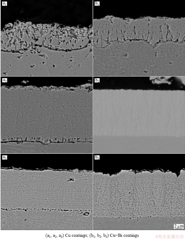
Fig. 1 SEM Cross-sectional morphologies of Cu and Cu-Bi coatings prepared at 10 mA/cm2 for 30 min (a1, b1), 50 mA/cm2 for 20 min (a2, b2), 100 mA/cm2 for 10 min (a3, b3)
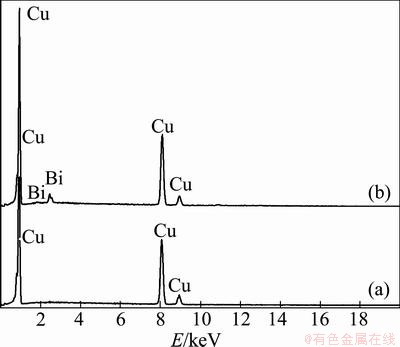
Fig. 2 EDS patterns of Cu coating (a) and Cu-Bi coating (b) prepared at 50 mA/cm2 for 20 min

Fig. 3 Content of Bi in Cu-Bi coatings prepared at different current densities
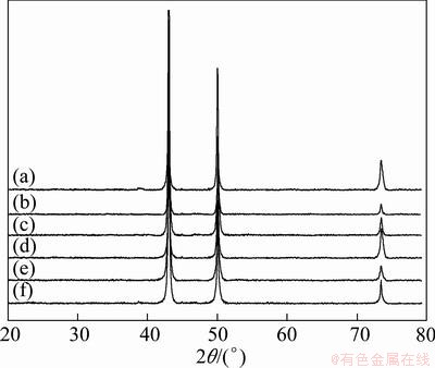
Fig. 4 XRD patterns of Cu (a, c, e) and Cu-Bi (b, d, f) coatings prepared at 10 mA/cm2 for 30 min (a, b), 50 mA/cm2 for 20 min (c, d), and 100 mA/cm2 for 10 min (e, f), respectively
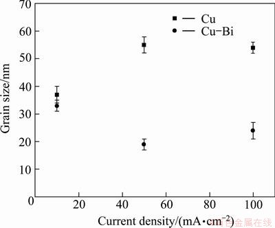
Fig. 5 Grain size in Cu and Cu-Bi coatings prepared at 10, 50 and 100 mA/cm2 for 30, 20 and 10 min, respectively

Fig. 6 Microhardness of Cu and Cu-Bi coatings prepared at 10, 50 and 100 mA/cm2 for 30, 20 and 10 min, respectively
Figure 7 shows the wear tracks of Cu and Cu-Bi composite coatings. The widths of wear tracks of Cu and Cu-Bi composite coatings prepared at 50 mA/cm2 for 20 min are ~150 ��m and 100 ��m, respectively. Many plough lines were observed on the surface of the Cu coating. In contrast, the wear tracks on the Cu-Bi composite coating were narrower and the plough lines were shallower, indicating that the Cu-Bi composite coating has improved wear resistance.
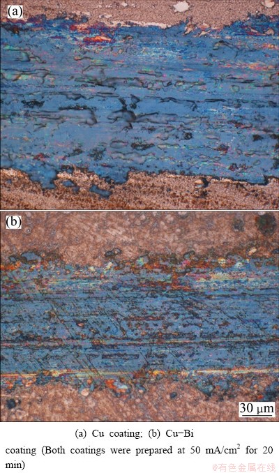
Fig. 7 Wear tracks on coatings
Figure 8 shows the coefficients of friction (COF) of Cu and Cu-Bi coating prepared at 50 mA/cm2 for 20 min. The COF of Cu coating started at ~0.45 and kept constant over time, while the COF of Cu-Bi coating started at ~0.25, and gradually developed to the level of ~0.40. COF is related to the roughness of the coating surface, and is also affected by the lubrication of the second phase. The low starting COF level of Cu-Bi coating may come from the relatively smooth surface of the Cu-Bi coatings. The higher COF value after few minutes sliding might be due to the formation of abrasive debris in the initial sliding.
3.4 Electrical resistivity
The electrical resistivities of Cu and Cu-Bi alloy samples are (2.31��0.06��10-8) ����m. Addition of Bi into the bath solutions did not bring any measurable effect on electrical resistivity. This is because Cu and Bi are insoluble metals. They do not form solid solution alloy so do not cause lattice distortion. The resistivity of two-phase structure is proportional to the volume percentage of the two phases [17,18]. In this research, the maximum content of Bi deposited in the Cu-Bi coating is just 3.1%. The volume fraction is even smaller. The Bi phase therefore does not affect the resistivity of Cu significantly.
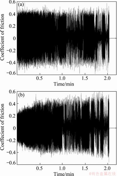
Fig. 8 Coefficient of friction of Cu coating (a) and Cu-Bi coating (b) prepared at 50 mA/cm2 for 20 min
4 Conclusions
1) Two non-solvable elements can make a metallic composite by electroplating method: a small amount of Bi has been added into Cu coatings to form a two-metal mixture.
2) The mechanical properties of the composite were improved significantly as the microhardness was improved from ~HV50 165 to ~HV50 250. Correspondingly, the wear resistance of the Cu-Bi composite coating has also been enhanced. XRD analysis indicates that the Bi addition does not cause lattice distortion of the Cu matrix; the electrical conductivity therefore has no measurable change. This Cu-Bi composite coating may extend the service life of Cu coatings when used as electric contacts.
Acknowledgements
The authors would like to thank the technical staffs of the Department of Chemical and Materials Engineering and the group members for their various assistances. Xiao-jin WEI appreciates the support from China Scholarship Council (CSC). See-Leng TAY thanks to Bright Sparks Unit, University Malaya for the financial support.
References
[1] DUNKLEY S F. The history and development of copper and its use as light-gauge tubes for domestic purposes [M]. London: Copper Development Association Publication, 1935.
[2] KIM M, SUN F F, LEE J, HYUN Y K, LEE D Y. Influence of ultrasonication on the mechanical properties of Cu/Al2O3 nanocomposite thin films during electrocodeposition [J]. Surface & Coatings Technology, 2010, 205(7): 2362-2368.
[3] ZHANG Yong-zhong, TU Yi, XI Ming-zhe, SHI Li-kai. Characterization on laser clad nickel based alloy coating on pure copper [J]. Surface & Coatings Technology, 2008, 202(24): 5924-5928.
[4] LIU Fang, LIU Chang-sheng, CHEN Sui-yuan, TAO Xing-qi, XU Zhi-feng, WANG Ming. Pulsed Nd:YAG laser post-treatment Ni-based crack-free coating on copper substrate and its wear properties [J]. Surface & Coatings Technology, 2007, 201(14): 6332-6339.
[5] 
 V. A study of copper coatings electrodeposited in electrolyte with a metallic powder of chromium [J]. Surface & Coatings Technology, 2006, 200(20-21): 6123-6129.
[6] NIKKOLA J, MANNILA J, MAHLBERG R, SIIVINEN J, KOLARI M, MAHIOUT A. Sol�Cgel based protective coatings for copper products [J]. Journal of Coatings Technology and Research, 2008, 5(3): 335-344.
[7] AVELAR-BATISTA J C, SPAIN E, LETCH M, HOUSDEN J, BEECHEY R. Improvements on the wear resistance of high thermal conductivity Cu alloys using an electroless Ni-P coating prior to PVD deposition [J]. Surface & Coatings Technology, 2006, 201(7): 4052-4057.
[8] PELLICER E, VAREA A,  S, SIVARAMAN K M, NELSON B J,
  M D, SORT J. A comparison between fine-grained and nanocrystalline electrodeposited Cu-Ni films. Insights on mechanical and corrosion performance [J]. Surface & Coatings Technology, 2011, 205(23-24): 5285-5293.
[9] MANGAM V, BHATTACHARYA S, DAS K, DAS S. Friction and wear behavior of Cu-CeO2 nanocomposite coatings synthesized by pulsed electrodeposition [J]. Surface & Coatings Technology, 2010, 205(3): 801-805.
[10] CHAKRABARTI D J, LAUGHLIN D E. The Bi-Cu (bismuth-copper) system [J]. Bulletin of Alloy Phase Diagrams, 1984, 5(2): 148-155.
[11] 
 R. Experimental study and thermodynamic remodeling of the Bi-Cu-Ni system [J]. Calphad, 2010, 34(3): 294-300.
[12] YUAN Guang-yin, SUN Yang-shan, DING Wen-jiang. Effects of bismuth and antimony additions on the microstructure and mechanical properties of AZ91 magnesium alloy [J]. Materials Science and Engineering A, 2001, 308(1-2): 38-44.
[13] LI Quan-an, ZHANG Qing, LI Chang-qing, WANG Yao-gui. Effects of Bi on mechanical properties of magnesium alloy AZ81 [J]. Advanced Materials Research, 2011, 284-286: 1693-1696.
[14] WANG Ya-xiao, ZHOU Ji-xue, WANG Jie, LUO Tian-jiao, YANG Yuan-sheng. Effect of Bi addition on microstructures and mechanical properties of AZ80 magnesium alloy [J]. Transactions of Nonferrous Metals Society of China, 2011, 21(4): 711-716.
[15] PATTERSON A L. The scherrer formula for X-ray particle size determination [J]. Physical Review, 1939, 56(10): 978-982.
[16] YAMANE T, KONDOU R, MAKABE C. Grain refinement and strengthening of a cylindrical pure-Aluminum specimen by using modified equal-channel angular pressing technique [J]. Key Engineering Materials, 2007, 340-341: 937-942.
[17] GAO Wei, LI Zheng-wei, SAMMES N. An introduction to electronic materials for engineers [M]. Singapore: World Scientific, 2011.
[18] ROSE R M, SHEPARD L A, WULFF J. Electronic properties [M]. New York: John Wiley & Sons Inc, 1966.
ͭ-����Ϳ��Ľṹ����ѧ����
κ����1����ΪΪ1��������1��֣˼��1,2���� Ψ1
1. �¿�����ѧ ��ѧ����Ϲ���ϵ��PB 92019���¿��� 1142����������
2. �����Ǵ�ѧ ��е����ϵ����¡�� 50603����������
ժ Ҫ�����õ�Ʒ����Ʊ�ͭ-�鸴��Ϳ�㡣��������ͭ�е��ܽ�ȼ��ͣ����Ϳ����������Ͻṹ���о�ͭ��ͭ-�鸴��Ϳ���еľ���ṹ�;������������Ϳ�����ѧ���ܣ�����ͭͿ������˱Ƚϡ������������Ʋ�����Ϳ�����ѧ����Ӱ��ϴ��ڵ����ܶ�Ϊ50 mA/cm2�����ʱ��Ϊ20 minʱ��ͭͿ���Ӳ��ΪHV50 165����ͭ-�鸴��Ϳ���Ӳ����ߵ�HV50 250��ͭ-�鸴��Ϳ�����ĥ��Ҳ��Ӧ��ߡ�
�ؼ��ʣ�ͭ-��Ϳ�㣻���϶Ʋ㣻Ӳ�ȣ�Ħ�����������
(Edited by Hua YANG)
Corresponding author: Wei GAO; Tel: +64-93737599-88175; Fax: +64-93737463; E-mail: w.gao@auckland.ac.nz
DOI: 10.1016/S1003-6326(13)62817-4